A 45nm Dual-Port SRAM with Write and Read Capability Enhancement
at Low Voltage
D.P. Wang
1,2, H.J. Liao
2, H. Yamauchi
3, Y.H. Chen
2, Y.L. Lin
2, S.H. Lin
2, D. C. Liu
2, H.C.
Chang
2, and W. Hwang
11
Institute of EE, National Chiao-Tung University; 2TSMC Hsinchu, Taiwan; 3Fukuoka Institute of Technology
E-mail: [email protected]
ABSTRACT
This paper presents circuit techniques to improve write and read capability for dual-port SRAM design fabricated in a 45nm low-power process. The write capability is enhanced by negative write biasing without any reduction in the cell current for the other port. The result shows 12% better improvement with just 1.9% area overhead. This technique has been verified successfully on 65nm and 45nm SRAM chip and improved 120mV lower at 95% yield of minimum operation voltage than a conventional one. The read capability is enhanced by cell current boosting and word line voltage lowering schemes. The SNM is also enhanced significantly. The target is to work below 0.8V with the worst process corner variation.
I. INTRODUCTION
As CMOS technology continues scaling down to 65nm and 45nm nodes, it is particularly difficult for SRAM design due to the fact that SRAM cell typically has more aggressive design rules and features than logic to meet stringent density requirement. Furthermore, with such a small cell size and high array density, device parameter fluctuation and characteristic variation become to impact to SRAM performance severely. Conventionally proposed raising up cell array’s VDD (CVDD) to CVDD_up at read cycle and lowering down to CVDD_down at write cycle is a common and acceptable technique for single-port SRAM. However it can not apply to dual-port SRAM design. Since dual-port SRAM operation needs to read and write at the same column for 2-port operating requirement, adjusting column based CVDD_up/down can just satisfy only one port need and is not suitable for the other port. Thus the three combinational techniques, negative-write and read boosting, and word-line lowering, have been developed for the first time, which can meet
read/write requirements simultaneously at the same column of dual-port SRAM operation.
II. NEGATIVE WRITE BIAS
Due to mismatch causing Vth of pass-gate NMOS of 8T dual-port SRAM cell rising, writing 0 into a bit-cell becomes difficult at low VDD condition for low Vgs. By applying a negative voltage to bit-line at this time [3], Vgs of pass-gate NMOS will enlarge again and pull down the storage node of bit-cell from logic 1 to logic 0 successfully while avoiding conventionally well known side-effects for “H”/-”L” read errors caused by CVDD_down and CVSS_up, respectively.
A negative voltage booster is combined with the local write buffer. Whenever a write enable signal of either A or B port activates the specified bank, its write buffer will pull down the corresponding bit-line to 0 in the first half period of a write pulse then start the booster to generate a negative pulse into bit-line in the second half period as Figure 1.
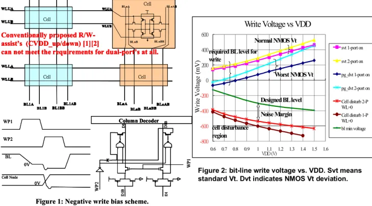
Figure 2 shows the required negative bit-line voltage for write vs. VDD for the normal and the worst cells. It is found that for the worst NMOS Vth shift, the bit-line voltage at a 1-port must become negative for VDD smaller than 0.8V to successfully flip the cell node. So applying negative bias into bit-line for write is the only way enabling to meet the dual-port read/write requirements.
Negative bit-line bias also keeps an advantage of lower VDD operation voltage than CVDD_down technique. For data retention reason, CVDD_down must keep a safe voltage margin above data retention voltage, otherwise, it will cause unselected cells disturbed. Allowing meshed power line of CVDD is also one of advantage. A characteristic comparison table between negative bit-line skill and CVDDLO technique is shown in table 1.
When a word line turns on, those on-cells will suffer stability issue. Especially at low VDD,
cells’ static noise margin degrade much. Adequately lowering word line voltage can gain back noise margin as shown in Figure 3. The circuitry for lowering word line voltage can be achieved by a voltage dividing technique.
In dual-port SRAM, a cell with both ports on will degrade SNM significantly. Meanwhile, if adequately lowering word line voltage to 0.9 times can almost recover SNM to original one as shown in the butterfly curves of Figure 4.
III. READ ENHANCING
With device mismatch, process variation, and word line lowering, the cell current may be not enough to sense out at a lower VDD condition. This paper proposes a negative voltage booster as Figure 5 to boost the selected column’s VSS to negative and therefore re-enhance the read current [4]. In an initial condition, all columns’ VSS connect to 0V. When either A or B port enables a column to read, it will start a negative booster to pull down the column’s VSS to negative and turn off the VSS control at the other port. If CVDD lowers, Vgs and current become small. The cell current can be recovered by lowering down VSS with a similar range to re-gain Vgs and then boost cell current. The negative bias for VSS is generated in the same manner as that for bit-line.
In a write cycle, bit-line pull down to negative and those unselected cells at the same column must take care of leakage causing cell data disturb. Also while reading one port and writing the same column at the other port, the column’s VSS pulling down to negative will cause another leakage source to make cells unstable. To avoid misleading the differentiation from the conventional ones, the following points are added: negative write bias and read enhancing techniques were independently proposed for a 0.25um process and before [3]-[4]. However, they did not consider any variation issue for dual-port at all. The proposed idea is integrating write and read concerns together and combining with statistical analysis for dual-port, that is an inventive step in design.
IV. SILICON EXPERIMENT
Regarding to negative write bias, Figure 6 shows an experiment result on 65nm. It shows that a single-port 2Mb SRAM chip with negative write function can work below 0.8V even though bit-cell’s
NMOS Vth 100mV weaker. In addition, Figure 7 shows comparisons between conventional ones and this work. It shows that the negative write biasing significantly improved 120mV Vddmin at low voltage on a 45nm dual-port SRAM chip as shown in Figure 7.
V. SUMMARY
This paper has presented the design techniques to enhance write and read capability on 1Mb dual-port SRAM chip using 45nm low-power process. The chip has been demonstrated that Negative write bias can improve write capability. Read current boosting can enhance read current and improve read capability. Lowering word line voltage can improve cell’s SNM. These ideas were implemented on a 45nm 1Mb dual-port SRAM chip. The chip size
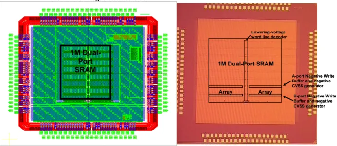
is 7.84mm2as shown in Figure 8.
REFERENCES
[1] K. Zhang, U. Bhattacharya, Z. Chen, F. Hamzaoglu, D. Murray, N. Vallepalli, Y. Wang, B. Zheng, M. Bohr, “A 3-GHz 70Mb SRAM in 65nm CMOS Technology with integrated Column-Based Dynamic Power Supply,” ISSCC Dig. Tech. Papers, pp 474-475, Feb. 2005.
[2] M. Yamaoka, K. Osada, and K. Ishibashi, “0.4-V Logic-Library-Friendly SRAM Array Using Rectangular-Diffusion Cell and Delta-Boosted-Array Voltage Scheme,” IEEE J. Solid-State Circuits, vol.39, pp. 934-940, June 2004.
[3] N. Shibata, H. Kiya, S. Kurita, H. Okamoto, M. Tan’no, and T. Douseki, “A 0.5-V 25-MHz 1-mW 256-Kb MTCMOS/SOI SRAM for Solar-Power-Operated Portable Personal Digital Equipment --- Sure Write Operation by Using Step-Down Negatively Overdriven Bitline Scheme,” IEEE JSSC, vol. 41, 2006, p728.
[4] H. Mizuno, and T. Nagano, “Driving Source-Line Cell Architecture for Sub-1-V High-Speed Low-Power Applications,” IEEE JSSC, vol. 31, 1996, p552.
SNM vs. VDD with WLx with variation
-50 0 50 100 150 200 0.6 0.7 0.8 0.9 1 1.1 1.2 1.3 1.4 VDD (V) SN M ( m V ) Vwl x 0.9 Vwl x 1Figure 3: SNM @6σ tail bit vs. word-line voltage Figure 1: Negative write bias scheme.
WP1 DL DL B D1 B D1 WP 2 WP1 WP2 BL Cell Node 0V 0V Column Decoder BLnA BLnBB BLnB BLnAB WLUA WLUB BLnA BLnAB BLnB BLnBB ˖˸˿˿ WLUA WLUB BLnA BLnAB BLnB BLnBB ˖˸˿˿ ˖˸˿˿ ˖˸˿˿ ˖˸˿˿ ˖˸˿˿ WLUA WLUB WLLA WLLB BL1A BL1B BLnB BLnA ˖˸˿˿ ˖˸˿˿ ˖˸˿˿ WLUA WLUB WLLA WLLB BL1A BL1BB BL1B BL1AB BLnA BLnBB BLnB BLnAB WLUA WLUB BLnA BLnAB BLnB BLnBB ˖˸˿˿ ˖˸˿˿ ˖˸˿˿ ˖˸˿˿ ˖˸˿˿ WLUA WLUB WLLA WLLB BL1A BL1B BLnB BLnA ˖˸˿˿ ˖˸˿˿ ˖˸˿˿ WLUA WLUB WLLA WLLB BL1A BL1BB BL1B BL1AB BLnA BLnBB BLnB BLnAB WLUA WLUB BLnA BLnAB BLnB BLnBB ˖˸˿˿ Conventionally proposed R/W-assist’s (CVDD_up/down) [1][2]
can not meet the requirements for dual-port’s at all.
Figure 1: Negative write bias scheme.
WP1 DL DL B D1 B D1 WP 2 WP1 WP2 BL Cell Node 0V 0V Column Decoder BLnA BLnBB BLnB BLnAB WLUA WLUB BLnA BLnAB BLnB BLnBB ˖˸˿˿ WLUA WLUB BLnA BLnAB BLnB BLnBB ˖˸˿˿ ˖˸˿˿ ˖˸˿˿ ˖˸˿˿ ˖˸˿˿ WLUA WLUB WLLA WLLB BL1A BL1B BLnB BLnA ˖˸˿˿ ˖˸˿˿ ˖˸˿˿ WLUA WLUB WLLA WLLB BL1A BL1BB BL1B BL1AB BLnA BLnBB BLnB BLnAB WLUA WLUB BLnA BLnAB BLnB BLnBB ˖˸˿˿ ˖˸˿˿ ˖˸˿˿ ˖˸˿˿ ˖˸˿˿ WLUA WLUB WLLA WLLB BL1A BL1B BLnB BLnA ˖˸˿˿ ˖˸˿˿ ˖˸˿˿ WLUA WLUB WLLA WLLB BL1A BL1BB BL1B BL1AB BLnA BLnBB BLnB BLnAB WLUA WLUB BLnA BLnAB BLnB BLnBB ˖˸˿˿ Conventionally proposed R/W-assist’s (CVDD_up/down) [1][2]
can not meet the requirements for dual-port’s at all.
WP1 DL DL B D1 B D1 WP 2 WP1 WP2 BL Cell Node 0V 0V Column Decoder WP1 DL DL B D1 B D1 WP 2 WP1 WP2 BL Cell Node 0V 0V Column Decoder BLnA BLnBB BLnB BLnAB WLUA WLUB BLnA BLnAB BLnB BLnBB ˖˸˿˿ WLUA WLUB BLnA BLnAB BLnB BLnBB ˖˸˿˿ ˖˸˿˿ ˖˸˿˿ ˖˸˿˿ ˖˸˿˿ WLUA WLUB WLLA WLLB BL1A BL1B BLnB BLnA ˖˸˿˿ ˖˸˿˿ ˖˸˿˿ WLUA WLUB WLLA WLLB BL1A BL1BB BL1B BL1AB BLnA BLnBB BLnB BLnAB WLUA WLUB BLnA BLnAB BLnB BLnBB ˖˸˿˿ ˖˸˿˿ ˖˸˿˿ ˖˸˿˿ ˖˸˿˿ WLUA WLUB WLLA WLLB BL1A BL1B BLnB BLnA ˖˸˿˿ ˖˸˿˿ ˖˸˿˿ WLUA WLUB WLLA WLLB BL1A BL1BB BL1B BL1AB BLnA BLnBB BLnB BLnAB WLUA WLUB BLnA BLnAB BLnB BLnBB ˖˸˿˿ Conventionally proposed R/W-assist’s (CVDD_up/down) [1][2]
can not meet the requirements for dual-port’s at all.
BLnA BLnBB BLnB BLnAB WLUA WLUB BLnA BLnAB BLnB BLnBB ˖˸˿˿ WLUA WLUB BLnA BLnAB BLnB BLnBB ˖˸˿˿ ˖˸˿˿ ˖˸˿˿ ˖˸˿˿ ˖˸˿˿ WLUA WLUB WLLA WLLB BL1A BL1B BLnB BLnA ˖˸˿˿ ˖˸˿˿ ˖˸˿˿ WLUA WLUB WLLA WLLB BL1A BL1BB BL1B BL1AB BLnA BLnBB BLnB BLnAB WLUA WLUB BLnA BLnAB BLnB BLnBB ˖˸˿˿ ˖˸˿˿ ˖˸˿˿ ˖˸˿˿ ˖˸˿˿ WLUA WLUB WLLA WLLB BL1A BL1B BLnB BLnA ˖˸˿˿ ˖˸˿˿ ˖˸˿˿ WLUA WLUB WLLA WLLB BL1A BL1BB BL1B BL1AB BLnA BLnBB BLnB BLnAB WLUA WLUB BLnA BLnAB BLnB BLnBB ˖˸˿˿ Conventionally proposed R/W-assist’s (CVDD_up/down) [1][2]
can not meet the requirements for dual-port’s at all.
Area penalty Noise tolerance (mesh power)
VDD min for
retention SOC friendly
Negative BL
small for each I/O mux
block
Good for VDD
keep meshed lower
Good for Metal4 as power mesh
routing
CVDDLO
large for each column mux pitch NG for no VDD mesh higher Power routing from metal5 Table 1
A Characteristic Comparison Table between Negative Bit-Line Skill and CVDDLO Technique.
Figure 4: SNM vs. VDD between Vwl and 0.9 * Vwl with cell Vt deviation; Butterfly curves of SNM number among 1-port on (100%), 2-port on (80%), and 0.9x word line voltage (100%). Dual-port Cell SNM 0 0.2 0.4 0.6 0.8 1 1.2 0 0.2 0.4 0.6 0.8 1 1.2 v(in) v( o ut ) out vs. in 1WL ON in vs. out 1WL ON out vs. in 2WL ON in vs. out 2WL ON out vs. in 2WL ON x09 in vs. out 2WL ON x09 Figure 2: bit-line write voltage vs. VDD. Svt means standard Vt. Dvt indicates NMOS Vt deviation.
Write Voltage vs VDD ˀˋ˃˃ʳ ˀˉ˃˃ʳ ˀˇ˃˃ʳ ˀ˅˃˃ʳ ˃ ˅˃˃ ˇ˃˃ ˉ˃˃ 0.6 0.7 0.8 0.9 1 1.1 1.2 1.3 1.4 1.5 1.6 ˩˗˗ʳʻ˩ʼ W ri te V o lta ge ( m V ) svt 1-port on svt 2-port on pg_dvt 1-port on pg_dvt 2-port on Cell disturb 2-P WL=0 Cell disturb 1-P WL=0 bl min voltage required BL level for
write Normal NMOS Vt Worst NMOS Vt Designed BL level Noise Margin cell disturbance region 213
cvss[0] ΞΞ cvss[n] ˖˸˿˿ ˖˸˿˿ ˖˸˿˿ ˖˸˿˿ Ay0B Ay0B By0B 0V negative voltage By0B Ay0B By0B 0V negative voltage cvss[0] ΞΞ cvss[n]
Figure 5: Read boost scheme.
700 800 900 1.00 103 1.10 103 1.20 103 1.30 103 1.40 103 .01 .1 1 5 10 20 30 50 70 80 90 95 99 99.9 99.99 T11(STD) ORG(STD) T11(N+100mv) ORG(N+100mv) mV P er c ent Conventional Proposed 750mV
Figure 6: 65nm silicon result on cumulative percentage vs. vdd min. T11 indicates 2Mb single-port SRAM with
negative write bias. ORG indicates normal 0V write voltage. Each dot indicates cumulative percentage of 2Mb SRAM chip pass yield at that vdd voltage.
Figure 7: 45nm silicon result on testing dual-port functional comparison with (left picture) and without (right picture) negative bit-line technique. Vddmin improved 120mV with negative write bias.
1.08 + + + + + 0.98 + + + + + + + c 1.06 + + + + + c 0.96 + + + + + + + v 1.04 + + + + + + v 0.94 + + + + + d 1.02 + + + + + + d 0.92 + + + + + d 1 + + + + + + d 0.9 + + + (V) 0.98 + + + + + + (V) 0.88 + + 0.96 + + + + 0.86 + 0.94 + + 0.84 0.92 + 0.82 0.9 0.8 0.88 0.9 0.92 0.94 0.96 0.98 1 1.02 1.04 1.06 1.08 0.78 0.8 0.82 0.84 0.86 0.88 0.9 0.92 0.94 0.96 0.98 Vdd (V) Vdd (V)
Figure 8: Layout plot and micrograph of 1Mb dual-port SRAM chip. 1M
Dual-Port SRAM
A-port Negative Write Buffer and negative CVSS generator
B-port Negative Write Buffer and negative CVSS generator
Array Array
Lowering-voltage word line decoder
1M Dual-Port SRAM
A-port Negative Write Buffer and negative CVSS generator
B-port Negative Write Buffer and negative CVSS generator
Array Array
Lowering-voltage word line decoder
1M Dual-Port SRAM