Easy Process and Performance Improvement for
Top-Emission Organic Light-Emitting Diodes
by Using UV Glue as the Insulation Layer
on Copper Substrate
Yu-Sheng Tsai, Shun-Hsi Wang, Fuh-Shyang Juang, Shu-Wei Chang, Chuan-hung Chen, Ming-Hua Chung,
Tsung-Eong Hsieh, Mark-O. Liu, and Teh-Chao Liao
Abstract—A high heat dissipation material (copper, Cu) was employed as the substrate for top emission organic light-emitting diodes (TEOLEDs). The UV glue was spin-coated onto the Cu substrate as the insulation layer to effectively improve Cu surface roughness and reduce process complexity. From the optoelectronic results, the optimized device with the Cu substrate shows the max-imum luminance of 14110 cd/m2and luminance efficiency of 7.14 cd/A. The surface and junction temperatures are measured to dis-cuss the heat-dissipating effect on device performance. From the results, TEOLED fabricated on a Cu substrate has lower junction (55.34 C) and surface (25.7 C) temperatures, with the lifetime extended seven times. We employed Cu foil as the substrate for flexible TEOLED with maximum luminance of 10310 cd/m2and luminance efficiency of 7.3 cd/A obtained.
Index Terms—Heat dissipation, junction temperature, lifetime, luminance efficiency, organic light-emitting diode (OLED), UV glue.
I. INTRODUCTION
T
HE organic light-emitting diode (OLED) [1] is a new-gen-eration flat panel display with the advantages of self-lumi-nescence, wide viewing angle ( ), prompt response time ( s), low operating voltage ( V), high luminanceManuscript received July 03, 2009; revised February 26, 2010; accepted April 05, 2010. Date of current version nulldate. This work was supported by the National Science Council under Project NSC-98-2221-E-150-008 and Project NSC-96-2221-E-150-025.
Y.-S. Tsai, s.-H. Wang, F.-S. Juang, S.-W. Chang, and C. Chen are with the Institute of Electro-Optical and Materials Science, National Formosa University, Huwei, Yunlin 63208, Taiwan (e-mail: ystsai@nfu.edu.tw; ac7174@hotmail. com; fsjuang@seed.net.tw; jimmys2home@hotmail.com; jarkvenber@yahoo. com.tw).
M.-H. Chung is with the Department of Materials Science and Engineering, National Chiao-Tung University, Hsinchu 30010, Taiwan, and also with the Ma-terial and Chemical Research Laboratories, Industrial Technology Research In-stitute, Hsinchu 30010, Taiwan (e-mail: itri950486@itri.org.tw)
T.-E. Hsieh is with the Department of Materials Science and Engineering, National Chiao-Tung University, Hsinchu 30010, Taiwan (e-mail: tehsieh@cc. nctu.edu.tw)
M.-O. Liu is with the Material and Chemical Research Laboratories, Industrial Technology Research Institute, Hsinchu 30010, Taiwan (e-mail: moliu@itri.org.tw)
T.-C. Liao is with the Department of Electro-Optical Engineering, National Formosa University, Huwei, Yunlin 63208, Taiwan (e-mail: techao@nfu.edu.tw)
Color versions of one or more of the figures in this paper are available online at http://ieeexplore.ieee.org.
Digital Object Identifier 10.1109/JDT.2010.2048300
efficiency, and high color purity that can be produced easily on various substrates. In recent years, much larger OLED dis-plays sizes have been fabricated. These large monitors must be driven using thin-film transistors (TFTs) that have even bright-ness, higher resolution, and longer life. Traditional OLED res-olutions are conducted mostly in the bottom emission structure and tend to be blocked by bottom TFTs and data lines, affecting ray penetration to the bottom. Top-emission OLED research has become inevitable for enhancing the opening rate [2], [3].
In this study, a high heat dissipation coefficient substrate (Cu: 401 W/m K) [4] is used to fabricate top-emission OLEDs (TEOLEDs). The heat-dissipation substrate will improve the OLED lifetime and performance. However, a copper (Cu) substrate surface is not completely smooth and will usually have spikes. After the OLED devices are evaporated onto the Cu substrate, the spikes will still exist. When the device is operated under high current density, a heavy amount of current density will concentrate at the spikes, leading to point discharge and damage to the device by causing the device to short circuit, generating joule heat [5]. The luminance efficiency and device lifetime will therefore be reduced. To improve the Cu substrate surface roughness, UV glue was spin-coated onto the Cu sub-strate as the insulation layer to effectively smooth the surface and significantly improve TEOLED lifetime and performances. In addition, Xi et al. have demonstrated that the diode forward voltage can be used to assess the junction temperature of “p–n junction diodes” [6]. The forward voltage method consists of two series of measurements: a calibration measurement and the actual junction–temperature measurement. The OLED is also a p-n junction diode, and the joule heat are generating at the in-terface of each layer during device (LED or OLED) operations. For this reason, the forward voltage method can be employed to measure the junction temperature of OLEDs.
Previous papers have reported that OLEDs fabricated onto flexible substrates using amorphous and TFTs onto flexible metal foils have propelled the development of flexible active matrix OLEDs (AMOLEDs) or active matrix polymer LEDs (AMPLEDs) displays [7]–[10]. Chuang et al. reported that the metal foils are particularly attractive for AMOLED or AMPLED displays because they are excellent barriers to water and oxygen which degrade the lifetime of these displays [7]. Hence, we fabricated the TEOLED device onto a flexible Cu foil substrate with spin-coated UV glue as the insulation layer.
II. EXPERIMENTAL
The OLED devices are generally fabricated onto glass and Cu substrates (39 mm 39 mm 0.5 mm). The heat transfer coefficient of Cu (purity: 99.9%), glass, and UV glue are 401, 1 [11], and 0.5 W/m K (supplied by Material and Chem-ical Research Laboratories, Industrial Technology Research Institute), respectively. Before depositing the metal anode, the substrate is cleaned ultrasonically with neutral cleaning agent (8 min), methanol (8 min) and deionized water (DI-Water) (8 min). The substrate is then dried via blown nitrogen and then placed into an oven for heating at 90 C for 10 min. The UV glue is then spin-coated onto the Cu substrate and cured using UV light for 10 s. The prepared substrate is next placed into a metal evaporation chamber; with Al (with high-reflectivity) and Au (with high work function) deposited under 4 10 torr to create an anode. The substrate is then moved into an or-ganic evaporation chamber for oror-ganic thin-films deposition under 2 10 torr. The hole-injection layer (HIL) is made of 4,4’,4’’-tris(N-3-methphenyl-N-phenyl-amino)-triph-enylamine (m-MTDATA), the hole transport layer (HTL) is N,N’-Bis(naphthalen-1-yl)-N,N’-bis (phenyl)–benzi-dine (NPB), and the emitting and electron transport layer (EML/ ETL) is tris(8-hydroxy-quinolinato)aluminum (Alq3). The device is next moved back into the metal evaporation chamber for metal cathode LiF/Al/Ag (semi-transparent) de-position. The total semi-transparent film thickness does not exceed 20 nm. The device active area is 36 mm . After the de-vice was fabricated, the SpectraScan PR650 and Keithley 2400 were employed to measure the optoelectronic characteristics. An infrared camera NEC TH9100 was employed to measure the substrate backside temperatures and thermal distribution images.
III. RESULTS ANDDISCUSSION
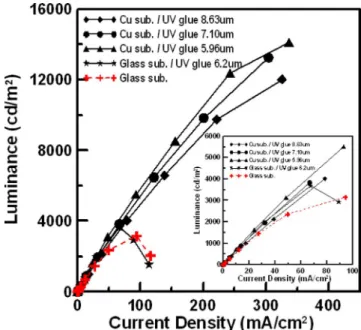
UV glue is spin-coated onto the Cu substrate (39 mm 39 mm 0.5 mm) using various rotation speeds to apply the UV glue evenly onto the substrate to create a flat Cu substrate surface. The UV glue also serves as the insulation layer. The insulation layer thickness is measured using -step. When the rotation speeds were 4000, 5000 and 6000 rpm, fixed at 10 s, the UV glue film thicknesses were 8.63, 7.10, and 5.96 m. Moreover, the surface roughness ( 0.312 nm) of glass with spin-coating UV glue is smoother than the bare glass substrate ( 1.07 nm), and the performances of device with UV glue were better than those without UV glue (as shown in Figs. 1 and 2). Hence, UV glue was also applied onto a glass substrate for comparison. At a rotation speed of 6000 rpm, fixed at 10 s, the UV glue film thickness on the glass substrate was 6.20 m. At rotation speeds of 4000 and 5000 rpm, the insulation layer is too thick. The Cu substrate surface is filled but the insulation layer surface is not smooth. The AFM images of insulation layer (UV glue) surfaces on the Cu substrate with different rotation speeds are shown in Fig. 3. When the rotation speed was increased to 6000 rpm, the insu-lation layer was thinner and the surface roughness decreased from 2.279 to 1.711 nm. Fig. 1 shows the luminance–current density ( – ) and Fig. 2 the luminance efficiency–current density ( – ) characteristics for different rotation speeds and
Fig. 1. L-J characteristics for different rotation speeds and substrates.
Fig. 2. Y –J characteristics for different rotation speeds and substrates.
Fig. 3. AFM images of insulation layer (UV glue) surfaces on the Cu substrate with different rotation speeds of: (a) 4000 rpm and (b) 6000 rpm.
substrates. The thinner insulation spin-coated onto the Cu substrate produced the maximum luminance 14110 cd/m and maximum luminance efficiency 7.14 cd/A.
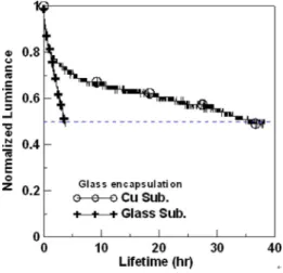
Fig. 4. Lifetime test of TEOLEDs with glass and Cu substrates.
Comparing the device characteristics between Cu and glass substrates (as shown in Figs. 1 and 2), devices fabricated onto a Cu substrate have better optoelectronic characteristics than those spin-coated onto glass substrates. We also found that the luminance and luminance efficiency (as shown in the inset of Figs. 1 and 2) of the devices with thicker insulation layer onto Cu substrate were lower than for device with thinner insulation layer on glass under low current density ( mA cm ). The reason is that the insulation layer surface is still rough when the insulation layer is too thick, leading to decreased TEOLED performance. However, the insulation layer surface roughness could be improved by decreasing the insulation layer thickness. Although a device with a thinner insulation layer has better lu-minance efficiency than devices with thicker insulation layers on Cu substrates under low operating conditions, the luminance efficiency decays quickly and breaks down under high current density. This is because the Cu substrate has a better heat con-ductivity coefficient (401 W/m K) than the glass substrate (1 W/m K). The joule heat can be dissipated quickly by the Cu sub-strate, preventing breakdown under high current density. From the lifetime tests shown in Fig. 4, the device lifetime when fabri-cated on a Cu substrate is seven times longer than that of device fabricated onto glass. This is attributed to the Cu substrate ef-fectively dissipating joule heat, preventing organic material re-crystallization.
To understand the joule heat effect on device performance, we measured the surface and junction temperatures [12], [13] of devices with different substrates. Table I shows the surface and junction temperatures of devices with Cu and glass substrates. When the operating current is increased, the surface tempera-ture of the glass substrate increases. The reason is that when the operating current is increased, a huge mass of joule heat accu-mulates at the device active area (with glass substrate), leading to the surface temperature increasing substantially. Conversely, the surface temperature of the Cu substrate exhibits only a small temperature increase because the joule heat is effectively dissi-pated by the Cu substrate. Comparing the highest surface tem-peratures of glass (57.8 C @ 40.98 mA) and Cu substrate de-vices (25.7 C @ 121.32 mA), the surface temperature of Cu substrate can be kept from 23 C to 26 C, prevented device breakdown.
TABLE I
MEASUREMENTSURFACE ANDJUNCTIONTEMPERATURES OFDEVICESWITH
CU ANDGLASSSUBSTRATES
Fig. 5. K curves for TEOLEDs with glass and Cu substrates.
To measure the TEOLEDs junction temperatures [6], [14], the devices were placed within a constant temperature oven to con-trol the initial environmental temperature ( C), and measure the corresponding forward voltage . The tem-perature was then increased to ( C). Each time, the temperature was increased 5 C in 5 min and then held for 6 min to reach a thermally stable status. During the 6-min tem-perature maintenance process, the device forward voltage ( ) under the maintained temperature was measured every 3 min. The measured device current was 0.01 mA. Fig. 5 shows the factor measured curves of for devices with glass and Cu sub-strates, respectively. The calculated factor values were auto-matically fitted using grapher software (dashed line). The fol-lowing equation was used for the calculation [12]–[14]:
(1) From the results, the curve slope for the Cu substrate device was more gradual than that for the glass substrate device. This proved that the Cu substrate could effectively dissipate the heat.
Therefore, the for the Cu substrate device decreased less than that for the glass substrate device.
After curve measurement, a constant measuring current ( mA) was then applied to the device to measure the corresponding forward voltage ( ). A high operating current was then applied (heating current, ). Once the device was operated for a while and the substrate temperature turned stable, the operating current ( ) was switched to , and its corresponding forward voltage was measured. is the device’s initial temperature prior to measurement (the envi-ronmental initial temperature was assumed to be 30 C in this study). Once the above values were obtained using [12]–[14]
(2) the junction temperature ( ) could be calculated for the de-vice under the operating current ( ): is the relative forward voltage at maximum temperature (50 C) at operation current 0.01 mA; is the device’s forward voltage at initial tempera-ture (30 C).
Table I shows a comparison of the junction temperatures for devices with Cu and glass substrates for different operating cur-rent (mA) conditions. The results show that when the glass sub-strate device was operated at 32.09 mA, the junction tempera-ture was 63.18 C. When the Cu substrate device was operated at the similar current of 33.43 mA, the junction temperature was only 36.98 C. After comparing the junction temperatures of the Cu and glass substrate devices, lower junction temperature for the device with the Cu substrate could be obtained under a similar operating current. This proved that the Cu substrate indeed could dissipate the heat effectively and quickly prevent breakdown.
We also employed Cu foil as the substrate for a flexible TEOLED to reduce the influence of joule heat. UV glue was spin-coated onto the Cu foil as an insulation layer to improve the foil surface roughness. The flexible TEOLED has a max-imum luminance of 10310 cd/m and luminance efficiency of 7.3 cd/A.
IV. CONCLUSION
A high heat-dissipation material (Cu) was successfully used as the substrate for a TEOLED. The Cu substrate reduces the influence of joule heat from devices operated under high current density. UV glue was spin-coated onto the Cu substrate as the insulation layer to effectively improve the roughness and reduced process complexity, providing significantly in-creased device lifetime and performance. At a rotation speed of 6000 rpm (10 s), the maximum luminance and efficiency were 14110 cd/m and 7.14 cd/A. From the – characteristic, the device luminance efficiency with a Cu substrate decayed slowly. We demonstrated better heat dissipation ability with a Cu substrate by comparing the thermal distribution images of TEOLED devices with Cu and glass substrates. The Cu substrate device surface temperature could be held to 25.7 C under high current density without breakdown. The surface temperatures of the glass substrate device increased from
29.1 C to 57.8 C when the junction temperature increased. From the junction temperature test, the device with the Cu substrate had lower junction temperature than the device with glass substrate under similar operating current. The Cu sub-strate device lifetime was about seven times longer than that for devices on glass substrates. We demonstrated that the Cu heat dissipation material can effectively dissipate joule heat and sig-nificantly improve the device performance and lifetime. Finally, we employed Cu foil as the substrate for flexible TEOLED and spin-coated UV glue onto the foil substrate as the insulation layer. The flexible TEOLED showed maximum luminance of 10310 cd/m and luminance efficiency of 7.3 cd/A.
REFERENCES
[1] C. W. Tang and S. A. VanSlyke, “Organic electroluminescent diodes,” Appl. Phys. Lett., vol. 51, pp. 913–915, Sep. 1987.
[2] M. Kitamura, T. Imada, and Y. Arakawa, “Organic light-emitting diodes driven by pentacene-based thin-film transistors,” Appl. Phys. Lett., vol. 83, pp. 3410–3412, Oct. 2003.
[3] D. Pribat and F. Plais, “Matrix addressing for organic electrolumines-cent displays,” Thin Solid Films, vol. 383, pp. 25–30, Feb. 2001. [4] C. Y. Ho, R. W. Powell, and P. E. Liley, “Thermal conductivity of the
elements,” J. Phys. Chem. Ref. Data, vol. 1, p. 279, 1972.
[5] C. R. Tsai, Y. S. Tsai, F. S. Juang, P. H. Yeh, Y. C. Chen, and C. C. Liu, “Top emission organic light-emitting diodes with double-metal-layer anode,” Jpn. J. Appl. Phys., vol. 46, pp. 2727–2730, Apr. 2007. [6] Y. Xi and E. F. Schubert, “Junction–temperature measurement in GaN
ultraviolet light-emitting diodes using diode forward voltage method,” Appl. Phys. Lett., vol. 85, pp. 2163–2165, Sep. 2004.
[7] T. K. Chuang, M. Troccoli, P. C. Kuo, A. J. Roudbari, M. K. Hatalis, I. Biaggio, and A. T. Voutsas, “Top-emitting 230 dots/in. active-matrix polymer light-emitting diode displays on flexible metal foil substrates,” Appl. Phys. Lett., vol. 90, p. 151114, Apr. 2007.
[8] S. D. Theiss and S. Wagner, “Amorphous silicon thin-film transistors on steel foil substrates,” IEEE Electron Device Lett., vol. 17, no. 12, pp. 578–580, Dec. 1996.
[9] M. Wu, K. Pangal, J. C. Sturm, and S. Wagner, “High electron mobility polycrystalline silicon thin-film transistors on steel foil substrates,” Appl. Phys. Lett., vol. 75, pp. 2244–2246, Oct. 1999.
[10] C. C. Wu, S. D. Theiss, G. Gu, M. H. Lu, J. C. Sturm, S. Wagner, and S. R. Forrest, “Integration of organic LEDs and amorphous Si TFTs onto flexible and lightweight metal foil substrates,” IEEE Electron Device Lett., vol. 18, no. 12, pp. 609–612, Dec. 1997.
[11] S. J. Chung, J. H. Lee, J. W. Jeong, J. J. Kim, and Y. T. Hong, “Sub-strate thermal conductivity effect on heat dissipation and lifetime im-provement of organic light-emitting diodes,” Appl. Phys. Lett., vol. 94, pp. 253302-1–3, Jun. 2009.
[12] J. G. Webster, Ed., The Measurement Instrumentation and Sensor Handbook Boca Raton, FL, CRC/IEEE, 1999.
[13] B. Siegal, “Measurement of junction temperature confirms package thermal design,” Laser Focus World, vol. 39, 2003.
[14] Y. S. Tsai, S. H. Wang, C. H. Chen, C. L. Cheng, and T. C. Liao, “Using copper substrate to enhance the thermal conductivity of top-emission organic light-emitting diodes for improving the luminance efficiency and lifetime,” Appl. Phys. Lett., vol. 95, pp. 233306-1–233306-3, Dec. 2009.
Yu-Sheng Tsai received the B.S. and Ph.D. degrees
in physics from National Tsing Hua University, Hsinchu, Taiwan, in 1983 and 1992, respectively.
He is currently with National Formosa University (NFU), Yunlin, Taiwan, as an Associate Professor with the Institute of Electro-Optical and Materials Science. From 1997 to 2000, he served as the chairman of the Department of Electro-Optics Engi-neering, NFU. Recently, his research activities have been in organic light-emitting diodes and organic solar cells.
Shun-Hsi Wang received the B.S. degree in
electrical engineering from Da Yeh University, Changhua, Taiwan, in 2004, and the M.S. de-gree from the Institute of Electrical-Engineering, Kun-Shan University, Yung Kang, Taiwan, in 2006. He is currently working toward the Ph.D. degree at the Institute of Electro-Optical and Materials Sci-ence, National Formosa University, Yunlin, Taiwan.
Recently, his research activities have been focused on organic light-emitting diodes.
Fuh-Shyang Juang was born in Tainan, Taiwan,
on July 30, 1964. He received the M.S. and Ph.D. degrees in electrical engineering from National Cheng Kung University (NCKU), Taiwan, in 1988 and 1991, respectively.
From 1995 to 2003, he was with the Department of Electro-Optics Engineering, National Huwei Institute of Technology (NHIT), as an Associate Professor and was engaged in research on compound semiconductor electrooptics materials and devices by metal–organic chemical vapor deposition. In 2003, he was promoted to Full Professor in the Department of Electro-Optics Engineering. From 2001 to 2002, he was on leave, studying GaN grown by molecular beam epitaxy with the University of California at San Diego, as a Visiting Scholar. From 2002 to 2008, he was the chairman in the Graduate In-stitute of Electro-Optical and Materials Science, National Formosa University (formerly NHIT). From February 2007 to February 2010, he was the Dean of the College of Electrical and Computer Engineering, NFU. Since February 2010, he has been the Dean of Office of Research and Development, NFU. Recently, his research activities have been focused on organic light-emitting diodes.
Dr. Juang was the recipient of the Award for Young People’s Paper, Excellent Engineering Paper Award, and the Excellent Professor Award from the Chinese Engineering Association in 1988, 2001, and 2007, respectively.
Shu-Wei Chang received the B.S. degree from in
mi-croelectronic engineering from National Kaohsiung Marine University, Kaohsiung, Taiwan, in 2007. He is currently working toward the M.S. degree at the In-stitute of Electro-Optical and Materials Science, Na-tional Formosa University, Yunlin, Taiwan.
Recently, his research activities have been focused on organic light-emitting diodes.
Chuan-hung Chen received the B.S. degree in
electrical engineering from Feng Chia Univer-sity, Taichung, Taiwan, in 2007. He is currently working toward the M.S. degree at the Institute of Electro-Optical and Materials Science, National Formosa University, Yunlin, Taiwan.
Recently, his research activities have been focused on organic light-emitting diodes.
Ming-Hua Chung was born in Tainan, Taiwan, on
February 10, 1968. He received the M.S. degrees in chemical engineering from Yuan Ze University, Taoyuan, Taiwan in 1996, and the Ph.D. degree from . the Department of Materials Science and Engi-neering, National Chiao Tung University (NCTU), Hsinchu, Taiwan, in 2009, where he studied the encapsulating technology of optoelectronic de-vices. [AUTHOR: PLEASE CLARIFY. DID
YOU RECEIVE THE PH.D. DEGREE FROM NCTU?—ED.]
From 2002 to 2004, he was with the Material Research Laboratories (MRL), Industrial Technology Research Institute (ITRI), Taiwan, as an Associate Re-searcher, where his work focused on the dispersion technology of functional polymers. He is currently with ???AU: PLEASE PROVIDE CURRENT
AF-FILIATION.
Tsung-Eong Hsieh received the M.S. degree
from the National Tsing-Hua University (NTHU), Hsinchu, Taiwan, in 1981, and the Ph.D. degree from the Massachusetts Institute of Technology (MIT), Cambridge, in 1988, both in materials engineering.
From 1989 to 2000, he was with the Department of Materials Science and Engineering of National Chiao-Tung University (NCTU), Hsinchu, Taiwan, as an Associate Professor. From 2000 to 2009, he was a Professor with the Department of Materials Science and Engineering, NCTU, where he special-ized in electronic packaging technology.
Mark-O. Liu was born in Kaohsiung, Taiwan, on
April 15, 1976. He received the B.S. degree from Na-tional Taiwan University (NTU), Taipei, in 1999, and the Ph.D. degree from National Tsing-Hua University (NTHU), Hsinchu, Taiwan, in 2004, both in chemical engineering.
From 2004 to 2009, he was with the Material and Chemical Research Laboratories (MCL), Industrial Technology Research Institute (ITRI) in Taiwan as a Researcher, where his work focused on the study of the syntheses as well as applications of optoelec-tronic polymers.
Teh-Chao Liao received the M.S. degree from
the Department of Optics and Photonics, National Central University, Taoyuan, Taiwan. He is currently working toward the Ph.D. degree at the Graduate School of Engineering Science and Technology, Na-tional Yunlin University of Science and Technology, Yunlin , Taiwan.
From 1991 to 1993, he served as the chairman of the Department of Electro-Optics Engineering, Na-tional Formosa University (NFU), Yunlin. He is cur-rently with NFU as a Lecturer with the Department of Electro-Optical Engineering.