0167-9317/$ - see front matter Ó 2007 Elsevier B.V. All rights reserved. doi:10.1016/j.mee.2007.04.127
www.elsevier.com/locate/mee Microelectronic Engineering 84 (2007) 1898–1901
Improvements of ozone surface treatment on the electrical
characteristics and reliability in HfO
2
gate stacks
Shih-Chang Chen
a,*, Yung-Yu Chen
b, Yu-Tzu Chang
a,
Jen-Chung Lou
a, Kon-Tsu Kin
c, Chao-Hsin Chien
a aInstitute of Electronics, National Chiao-Tung University, Hsinchu 300, TAIWAN
b
Computer Science and Information Engineering, Yuanpei University, Hsinchu 300, TAIWAN
c
Energy and Environment Research Laboratories, Industrial Technology Research Institute, Chutung 310, TAIWAN
Abstract
In this study, we improved the interfacial properties of high-ț gate stacks with the surface treatment of ozonated water prior to deposition of hafnium oxide (HfO2). We demonstrated that the Ozone-oxide improved the electrical properties of the HfO2 gate stack interface in terms of its smoother interface, lower leakage current density, narrower hysteresis width, superior charge trapping effect, and reliability. From these experimental results, we believe that treatment with ozone is an efficient method for the preparation of high-quality interfaces between HfO2 and silicon surfaces.
Keywords: high-ț; ozone; surface treatment; charge trapping; reliability.
1. Introduction
Direct deposition of high-permittivity (high-N) dielectrics on silicon surface will inevitably deteriorate device performances and reliability characteristics [1]. Therefore, surface treatments prior to high-N deposition are considered to be necessary in order to enhance the capabilities of high-N gate stack. Treatment with ozonated water has
Corresponding author. Tel.:+ 886 3 5712121 ext.54184;
fax: + 886 3 5724361
E-mail address:scchen.ee92g@nctu.edu.tw (Shih-Chang
Chen)
been utilized to deposit ultrathin oxide layers (<10 Å) at low temperatures (nearly room temperature) [2]. The growth of the ozonic oxide occurs in a layer-by-layer manner, with a thinner transition layer-by-layer. [3]. The ozonic oxide is homogeneous from the surface to the interface, unlike corresponding thermal oxide layers [3]. Moreover, the density of an ozonic oxide is, however, comparable to that of a thick thermal oxide [3]. Our aim for this experiment was to use ozonated water treatment to improve the quality of HfO2/Si
interface. Furthermore, we also systematically investigated the trapping effects and reliability in ozone pre-treated HfO2.
S.-C. Chen et al. / Microelectronic Engineering 84 (2007) 1898–1901 1899
2. Experimental
After standard RCA processes, the p-type (100) silicon wafers were treated using ozone oxidation (Ozone), rapid thermal oxidation (RTO, 800 °C), and ammonia nitridation (NH3, 800 °C, furnace). Diluted
ozonated water was used to grow an ultrathin ozonic oxide at room temperature (ca. 7-8 Å, measured by ellipsometer). Thin SiO2 layer (ca. 10 Å ) and thin
oxynitride layer (ca. 10 Å) grew in RTO and NH3
nitridation, respectively. After each of these surface treatments, a 55Å-thick HfO2 layer was deposited at
500 °C using an MOCVD system, followed by high-temperature post-deposition annealing (PDA) at 600 °C in a nitrogen ambient for 30 s. Aluminum metal, which served as the gate electrode, was created using a thermal evaporation system. After the gate electrodes had been patterned and the contact holes etched, metallization and backside contact were performed, followed by sintering at 450 °C.
3. Results and discussion
Fig. 1 displays the growth rates of the ozone-mediated oxide as a function of the concentration of ozone in the water. The ozone-mediated oxidation revealed a specific property of self-limited growth, which provided an ultrathin surface oxide (<10 Å) that was a necessary requirement prior to high-N dielectric deposition; not only was this oxide ultrathin, it was also of high quality.
Growth Time (min)
0 1 2 3 4 5 O z one O x id e Thi cknes s (A) 0 2 4 6 8 10 10 ppm 5 ppm 2 ppm 1 ppm
Fig. 1. Growth curves of ozone-mediated oxides plotted as a function of the concentration of ozone in water.
In Fig. 2, from comparisons of the etching rate we observe a high film density of the ozone-mediated oxide because of the extremely low etching rate near the SiO2/Si interface. This superior film density
originated from the layer-by-layer growth of the ozone-mediated oxidation process [3].
HF : H2O = 1 : 500
Etching Time (sec)
0 20 40 60 80 100 120 140 160 O xi d e Thi c knes s ( A ) 0 2 4 6 8 10 Chemical Oxide Ozone Oxide Etching Rate 1 2.09A/min Etching Rate 1 2.66A/min Etching Rate 2 4.16A/min Etching Rate 2 1.01A/min
Fig. 2. Comparison of the etching rates at HF:H2O = 1:500 of the ozone-mediated oxide to that of the chemical oxide formed by RCA cleaning without HF-last.
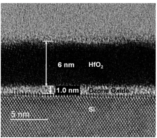
Fig. 3 presents a high-resolution TEM image in which we observe a thin Ozone-SiO2 layer (< 10 Å)
and smooth ozone-SiO2/Si and HfO2/Ozone-SiO2
interfaces. We can observe that the Ozone-SiO2 layer
remained amorphous after PDA at 600 °C.
5 nm Si HfO2 Ozone Oxide 5 nm Si HfO2 Ozone Oxide
Fig. 3. HRTEM image of the ozone-treated HfO2 after PDA at 600 °C.
1900 S.-C. Chen et al. / Microelectronic Engineering 84 (2007) 1898–1901
Appropriate surface treatment prior to high-N deposition is necessary to improve the high-N/Si interface characteristics. Fig. 4 demonstrates the effects of surface treatments on the leakage current density of 600 °C - PDA HfO2. Both NH3 and Ozone
treatment suppressed leakage current of the stacked gate dielectric relative to that of a sample that was not subjected to surface treatment. The lower leakage current of ozone treatment is considered to be partial due to the formation of smoother interfaces [4].
PDA 600oC Samples
Effective Electric Field ( MV/cm )
0 10 20 30 40 Leakage Cur rent Densit y ( A/ cm 2 ) 10-10 10-9 10-8 10-7 10-6 10-5 10-4 10-3 10-2 10-1 100 101 102 w/o S.T. ( EOT = 24.42 A ) NH3 ( EOT = 25.83 A ) RTO ( EOT = 25.63 A ) Ozone ( EOT = 26.59 A )
Fig. 4. Leakage current density of HfO2 gate stacks with respect to the various surface treatment processes.
Although surface nitridation also reduced the gate leakage current, degradation of the interfacial properties was inevitable; for example, C-V deterioration is apparent for the NH3-treated sample
in Fig. 5. The significant negative C-V shift indicates that positive charges arising from the interfacial Si-N layer after surface nitridation [5]. On the other hand, both the RTO- and Ozone-treated samples exhibited negligible interfacial reactions and VFB shifts,
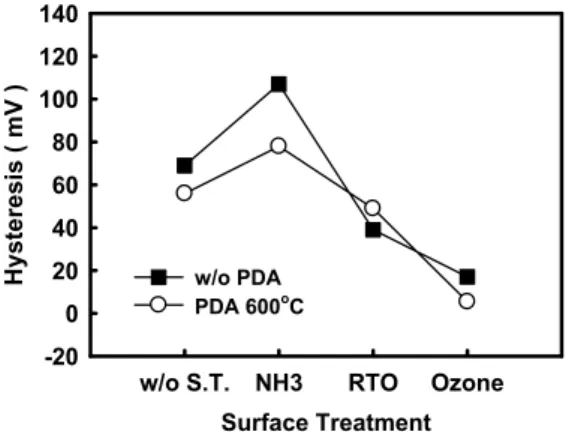
demonstrating that surface oxidation provided interfaces that were superior to those formed after surface nitridation. Fig. 6 displays the hysteresis curves of the various samples. The sample that had not been subjected to surface treatment and that which had been subjected to NH3-mediated
nitridation both exhibited large degrees of hysteresis, which were enhanced slightly further after high-temperature PDA. Fortunately, surface oxidation resulted in excellent hysteresis behaviors. Especially, the Ozone-treated sample exhibited almost hysteresis-free feature. PDA 600oC Samples Gate Voltage ( V ) -3 -2 -1 0 1 Normalize d Capacit a nc e ( pF ) 0.0 0.2 0.4 0.6 0.8 1.0 1.2
w/o Sur. Treat. NH3
RTO Ozone
Fig. 5. C-V characteristics of HfO2 stacked gate dielectrics with respect to various surface treatment processes.
Surface Treatment
w/o S.T. NH3 RTO Ozone
Hys teres is ( mV ) -20 0 20 40 60 80 100 120 140 w/o PDA PDA 600oC
Fig. 6. Hysteresis curves obtained with respect to the various surface treatment processes.
Charge trapping phenomena in high-N dielectrics will have great influences on the electrical characteristics and reliabilities of MOSFETs devices [6]. Fig. 7 and Fig. 8 demonstrated the influences of surface treatments on charge trapping effect. We observe that each of the surface treatment processes improved the value of 'VFB. In particular, treatment
with ozone provided excellent experimental results, which we attribute to the superior interfacial quality that ascribing to the layer-by-layer and homogeneous growth from the surface to the interface. Furthermore, the Ozone-treated sample exhibited the lowest trapping effects, consistent with the its improved interfacial properties and lower value of 'VFB, The
results demonstrated that a superior interfacial quality of ozone-mediated oxide can efficiently
S.-C. Chen et al. / Microelectronic Engineering 84 (2007) 1898–1901 1901
improve the charge trapping effect in such high-ț gate stack.
PDA 600oC Samples
Stress Time (sec)
100 101 102 103 104 ' VFB (mV) -400 -300 -200 -100 0 100 w/o Treatment NH3 RTO Ozone CVS = - 3.8 V
Fig. 7. Plots of 'VFB under a CVS of –3.8 V with respect to the various surface treatment processes.
PDA 600oC Samples CVS = - 3.8V Injected Charges (C/cm2) 10-4 10-3 10-2 10-1 100 Trap pe d C har ges ( 1 0 11 /cm 2 ) 0 4 8 12 16 20 24 28 w/o Sur.Treat. NH3 RTO Ozone
Fig. 8. Charge trapping effects plotted with respect to the various surface treatment processes.
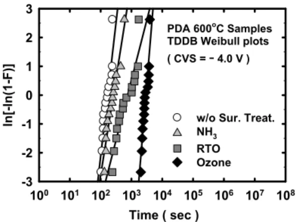
In addition, the reliability was investigated through the behaviors of time-dependent dielectric breakdown (TDDB) in Fig. 9. After surface treatment, the interface qualities improved to enhance the device reliabilities, with the Ozone-treated sample exhibiting superior performance in this TDDB investigation relative to those of the other surface-treated samples. These reasonable experimental results were not only consistent with the other electrical characteristics but also explain that less charge trapping in the ozone surface treatment can effectively improve the reliability characteristics. PDA 600oC Samples TDDB Weibull plots ( CVS = - 4.0 V ) Time ( sec ) 100 101 102 103 104 105 106 107 108 ln[-ln(1-F )] -3 -2 -1 0 1 2 3
w/o Sur. Treat. NH3
RTO Ozone
Fig. 9. Investigations of reliability obtained in TDDB measurements with respect to the various surface treatment processes.
4. Conclusions
In this study, we systematically investigated the basic properties of ozone-mediated oxide growth. The low temperature (RT) employed, the slow growth rate, and the self-limiting growth process all provided an ultrathin oxide (<10 Å) of high density and excellent quality, which can be utilized to improve the properties of the HfO2/Si interface. The
ozone-treated samples exhibited better interfacial properties, a smaller leakage current, negligible hysteresis, lower charge trapping effects and excellent dielectric reliability than did the NH3 and
RTO surface-treated systems. Consequently, this technique should be considered when attempting to improve the interfacial properties between high-N dielectrics and silicon surfaces.
References
[1] G. D. Wilk, R. M. Wallace, J. M. Anthony, J. Appl. Phys. 89 (2001) 5243-5275.
[2] W. Howard Thompson, Zain Yamani, Laila H. Abu Hassan, J. E. Greene, Munir Nayfeh, M.-A. Hasan, C. C. Camero J. Appl. Phys. 80 (1996) 5415-5421. [3] S. Ichimura, A. Kurokawa, K. Nakamura, Thin Solid
Films 377-378 (2000) 518-524.
[4] Y. Y. Chen, C. H. Chien, J. C. Lou, Jpn. J. Appl. Phys. 44 (2005) 1704-1710.
[5] P. J. Wright, A. Kermani, K. C. Saraswat, IEEE Trans. Electron Dev. 37 (1990) 1836-1841.
[6] S. Zafar, A. Kumar, E. Gusev, E. Cartier, IEEE Trans. Dev. Mater. Reliability. (TDMR) 5 (2005) 45-64.