This content has been downloaded from IOPscience. Please scroll down to see the full text.
Download details:
IP Address: 140.113.38.11
This content was downloaded on 26/04/2014 at 05:30
Please note that terms and conditions apply.
Evidence for the electron trap state associated with N-rich clusters in InGaAsN/GaAs quantum
wells
View the table of contents for this issue, or go to the journal homepage for more
2007 Nanotechnology 18 235402
(http://iopscience.iop.org/0957-4484/18/23/235402)
Nanotechnology 18 (2007) 235402 (5pp) doi:10.1088/0957-4484/18/23/235402
Evidence for the electron trap state
associated with N-rich clusters in
InGaAsN/GaAs quantum wells
J F Chen
1, P C Hsieh
1, R S Hsiao
1, J S Wang
2and J Y Chi
31Department of Electrophysics, National Chiao Tung University, Hsinchu, 30010 Taiwan, Republic of China
2Department of Physics, Chung Yuan Christian University, Chung-Li, 32023 Taiwan, Republic of China
3Industrial Technology Research Institute (OES/ITRI), Hsinchu, 310 Taiwan, Republic of China
E-mail:jfchen@cc.nctu.edu.tw
Received 7 February 2007, in final form 20 March 2007
Published 8 May 2007
Online at
stacks.iop.org/Nano/18/235402
Abstract
An electron trap state has been found to appear in InGaAsN/GaAs quantum
wells (QWs) as a result of composition fluctuation. Evidence of composition
fluctuation is shown by photoluminescence spectra which display an
additional low-energy emission due to local regions of N-rich clusters.
Enhancing composition fluctuation leads to undulated InGaAsN/GaAs
interface with dot-like islands. The capacitance–voltage profiling shows an
additional peak following the QW electron ground state peak, suggesting the
presence of an electron trap state below the QW electron ground state. The
emission properties of this trap state are similar to those of quantum dots
immersed in a well. Enhancing composition fluctuation can cause an energy
downward shift and spectral broadening of this electron trap state, suggesting
an increase in island size and fluctuations of the size and composition. Thus,
it is deduced that the electron trap state originated from the N-rich clusters in
the well behaving like quantum dots. Upon modulation, the electrons are
thermally activated from this trap state to the QW electron ground state and
subsequently emitted to the GaAs bottom electrode.
1. Introduction
Long wavelength lasers made of InGaAsN/GaAs quantum wells (QWs) are promising for optical fibre communica-tion [1–8]. However, N incorporation often induces recombi-nation centres [9–11] which degrade photoluminescence (PL) efficiency [12, 13]. Increasing growth temperature may al-leviate this problem but often leads to composition fluctua-tion [14–17]. Evidence of composition fluctuation or cluster-ing has been shown by PL spectra [14–18] and transmission electron microscopy (TEM) [17]. Many authors have observed anomalous S-shaped temperature dependence of the emission energy and attributed it to an exciton localization effect due to composition fluctuation [19,20]. Enhancing composition fluc-tuation can lead to strong carrier localization and quantum-dot (QD)-like behaviour [21, 22]. Recently, near-field
magneto-photoluminescence spectroscopy is used for the estimation of the size, density and depth of these QD-like compositional fluc-tuations [21, 23, 24]. Despite these achievements, detailed properties of electron emission from these QD states have not been investigated. Understanding this effect is essential not only for physical interest but also for device applications. We have previously shown that lowering the growth rate of the In-GaAsN layer degraded PL efficiency and caused electron de-pletion [25] due to enhanced composition fluctuation. We con-tinue this study by using capacitance–voltage (C–V) profiling and admittance spectroscopy on samples with different degrees of composition fluctuation. Composition fluctuation is shown to induce an electron trap state which can partially trap elec-trons in the well. Enhancing composition fluctuation can shift downward and broaden the electron trap state. This dot-like behaviour suggests that the electron trap state is induced by N
Nanotechnology 18 (2007) 235402 J F Chen et al
clusters acting like quantum dots. Possible energy position of the electron trap state and its likely emission process are dis-cussed.
2. Experimental details
The GaAs/InGaAsN/GaAs single-quantum-well (SQW) sam-ples were grown on n+-GaAs(001) substrates by molecular beam epitaxy equipped with an EPI-Unibulb radio frequency (RF) plasma source to provide nitrogen species from pure N2
gas. Indium and gallium were supplied from conventional K cells and As in the form of As2 was supplied from a cracker
source. The growth was started with a 0.3μm Si-doped GaAs layer of∼6×1016cm−3grown at 580◦C, followed by a 60 ˚
A-thick InGaAsN layer, grown at 420◦C. To avoid introducing shallow impurities, the InGaAsN layer was undoped. After the growth of the InGaAsN layer, the growth temperature was in-creased to 580◦C for the growth of a 0.3μm Si-doped GaAs top layer of∼6×1016cm−3. The In and N compositions were
obtained from fitting the x-ray diffraction spectra by first deter-mining the In composition from an InGaAs/GaAs SQW struc-ture and then determining the N composition, assuming the In composition remained unchanged. Detailed growth conditions can be found elsewhere [26,27]. To enhance composition fluc-tuation, the growth rate of the InGaAsN layer was lowered from 4.4 to 0.5 ˚A s−1by scaling down the In and Ga fluxes. Due to a difficulty in precisely adjusting the N beam flux, the samples grown at different growth rates may have slightly dif-ferent N compositions. Schottky contacts were fabricated by evaporating Al with a dot diameter of 800μm. PL spectra were obtained by a frequency doubled YAG:Nd laser (λ =532 nm) and an InGaAs detector.
3. Results and discussions
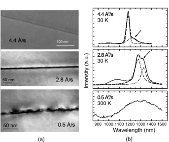
Lowering the growth rate of the InGaAsN layer enhances composition fluctuations [25]. Figure 1(a) shows the cross section TEM images of the InGaAsN/GaAs SQW samples with the InGaAs layers grown at 4.4, 2.8 and 0.5 ˚A s−1, respectively. In each sample, the In and Ga compositions are 34% and 66%, respectively. The N composition is 1.6% for the 4.4 ˚A s−1sample and 2% for 2.8 and 0.5 ˚A s−1samples. The InGaAsN layer is clearly visible in each sample. A slight degradation of interface sharpness can be seen when lowering the growth rate from 4.4 to 2.8 ˚A s−1. With a further lowering to 0.5 ˚A s−1, a rather undulated upper interface with small dark islands can be seen. Reflection high-energy electron diffraction (RHEED) platters turned spotty in this sample, suggesting a transition to three-dimension (3D) growth mode. Similar 3D islands were observed in InGaAsN/GaAs QWs [17] and were attributed to composition fluctuation. To evaluate the optical properties, figure1(b) shows the PL spectra of the investigated samples under an excitation power of 1.3 mW for the 4.4 ˚A s−1 sample and 325 mW for the 2.8 ˚A s−1and 0.5 ˚A s−1samples, respectively. The main peak is related to QW emission. As previously reported [25], lowering the growth rate considerably degrades the QW emission. The wavelength redshift (from 1183 to 1275 nm) from the 4.4 to 2.8 ˚A s−1 sample is due to an increase of N composition from 1.6 to 2%, which also contributes to composition fluctuation. The 2.8 ˚A s−1
(a) 900 1000 1100 1200 1300 1400 1500 2.8 Ao /s 30 K 0.5 Ao /s 300 K 4.4 Ao/s 30 K (b) 2.8 Ao /s Intensity (a.u.) 0.5 Ao /s Wavelength (nm) 4.4 Ao/s
Figure 1. (a) Cross-sectional TEM images of the InGaAsN SQW
samples with the InGaAs layer deposited at 4.4 ˚A s−1, 2.8 ˚A s−1and 0.5 ˚A s−1, respectively. Flat interfaces in the 4.4 and 2.8 ˚A s−1 samples and rather undulated interfaces with 3D dark islands in the 0.5 ˚A s−1sample can be seen. (b) PL spectra of the corresponding samples. Beside the QW emission, a low-energy peak (indicated by arrows) due to composition fluctuation can be seen in the 4.4 and 2.8 ˚A s−1samples. Further lowering to 0.5 ˚A s−1severely degrades the PL spectra.
sample displays a broad emission at ∼1075 nm which is due to recombination of a deep level (detailed properties will be published elsewhere). The spectrum of the 4.4 ˚A s−1 sample displays a low-energy tail (indicated by an arrow). This tail often observed in N–As alloys was attributed to the recombination of excitons trapped by localized states at the band tail induced by composition fluctuation [16]. By fitting the spectrum to two Gaussian curves, this low-energy tail is about 30 meV separated from the QW emission. When composition fluctuation is enhanced by lowering the growth rate to 2.8 ˚A s−1, this tail becomes a pronounced shoulder with intensity comparable to that of the QW emission. By fitting, this low-energy peak is separated from the QW emission by about 38 meV. The lower emission energy suggests the presence of local regions with N composition higher than the average, i.e. N-rich clusters [16]. With a further lowering to 0.5 ˚A s−1, the QW emission becomes very weak and broad (centred on 1300 nm). At low temperatures, the spectrum is dominated by the deep-level emission around 1075 nm. These results show an enhancement in composition fluctuation from the 4.4 to 2.8 and to 0.5 ˚A s−1 samples. It should be noted that, in order to retain the composition fluctuation, the studied samples are not annealed after growth. However, considerable improvement of the QW emission and suppression of the N-rich low-energy tail are observed in the 2.8 ˚A s−1sample after post-growth rapid thermal annealing at 700◦C for 5 min. This result further supports that the low-energy tail is due to composition fluctuation, since annealing is known to effectively alleviate composition fluctuation.
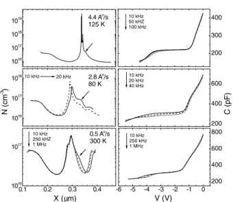
Figure2 shows theC–V spectra and the corresponding apparent-carrier-concentration profiling of the investigated samples. The concentration peak at∼0.3μm (C–V step at
−2 V) is related to the depopulation of the QW electron ground 2
1016 1017 1018 1019 1016 1017 1018 200 300 400 0.1 0.2 0.3 0.4 1016 1017 -6 -5 -4 -3 -2 -1 0 200 400 600 800 200 400 600 4.4 Ao /s 125 K 20 kHz 2.8 Ao /s 80 K N (cm -3 ) 10 kHz 10 kHz 50 kHZ 100 kHz 0.5 Ao/s 300 K X (μm) 10 kHz 250 kHZ 1 MHz V (V) 10 kHz 250 kHz 1 MHz C (pF) 10 kHz 20 kHz 40 kHz
Figure 2.C–V spectra and their converted
apparent-carrier-concentration profiles of the investigated samples. The C–V plateau around−2 V and the corresponding peak around 0.3 μm are due to the discharging of the QW. The additional C–V plateau around−4 V and the corresponding peak (indicated by arrows) suggest the presence of an electron trap state below the QW electron ground state. The frequency-dependent dispersions suggest a restively long emission time for this state.
state (EGS). The peak increases its intensity with lowering temperature, suggesting a Debye-length quantum effect. This peak suffers no frequency-dependent attenuation up to 1 MHz at 10 K, suggesting a very short emission time. The narrowest linewidth in the 4.4 ˚A s−1 sample is consistent with the strongest QW emission. When the dc voltage is decreased to about−4 V, another peak emerges at the right shoulder of the QW peak (indicated by arrows). This indicates the presence of an electron trap state below the QW EGS. The area under the peak is indicative of the density of the state. As shown, this area increases from the 4.4 to 2.8 ˚A s−1samples, consistent with an enhanced composition fluctuation. Note that this state is not associated with dopant-related shallow impurities since the InGaAsN layer is undoped.
Figure2shows frequency-dependent attenuation for the right-shoulder carrier peak, suggesting an observable electron emission time for the trap state. The emission time is inves-tigated by means of admittance spectroscopy [25]. Figure3
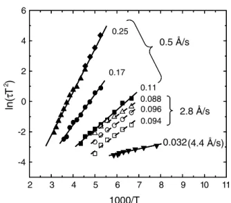
shows the conductance/frequency–frequency (G/F–F) spec-tra, measured at the dc bias corresponding to the right-shoulder carrier peak. Each sample displays a peak at a frequency com-parable to the inverse of the emission time. Figure4shows the Arrhenius plots of their emission times from which we obtain an activation energy (capture cross section) of 32±24 meV (1.3× 10⁻¹⁸ cm2) for the 4.4 ˚A s−1 sample. The
activa-tion energy (capture cross secactiva-tion) of the 2.8 ˚A s−1 sample shows a slightly dc bias dependence, which increases from 88 (5.2×10⁻¹⁸cm2) to 94 meV (2.7×10⁻¹⁷cm2) from−3 to −4.5 V. Beyond−4.5 V, the conductance peak rapidly dimin-ishes due to the emptying of electrons in the trap state and no reliable data could be obtained. In view of the close proxim-ity between the right-shoulder carrier peak and the QW peak (in figure2), we place the electron state at the obtained
acti-104 105 106 100 200 0 100 200 103 104 105 106 0 50 100 150 225 K 4.4 Ao /s (-3.5V) 125 K 200 K 80 K G/f (pS/Hz) 2.8 Ao/s (-4V) 280 K 190 K f (Hz) 0.5 Ao/s (-3.5V)
Figure 3. Temperature-dependent G/F–F spectra, measured at the
dc voltage corresponding to the electron trap state (indicated by arrows in figure2). Each curve displays a peak at a frequency comparable to the inverse of the emission time. The analysis of
G(F) and G(T ) allows us to determine the emission time as a
function of temperature.
vation energy below the QW EGS as shown in the electronic structure in figure5, where the conduction-band band offset is estimated to be∼0.3 eV [18, 29] from the QW emission energy. Upon modulation, we speculate that electrons are ther-mally activated from the electron state to the QW EGS and sub-sequently activated to the bottom GaAs electrode. The short emission time for the latter process was not resolved, as there was no frequency-dependent attenuation in the QW peak up to 1 MHz at 10 K.
The admittance spectroscopy indicates that the energy difference between the electron state and the QW EGS is 32 meV in the 4.4 ˚A s−1sample which increases to∼88 meV in the 2.8 ˚A s−1sample. These values are comparable with the energy spacing (30–38 meV) between the PL low-energy tail and the QW emission (in figure1(b)), strongly suggesting that the electron state causes the low-energy PL emission. This correlation is further supported by the fact that both are observed at low temperatures and simultaneous enhancement in the right-shoulder carrier peak and the low-energy PL emission from the 4.4 to 2.8 ˚A s−1samples. It should be noted that our observed energy spacing of 30–38 meV is comparable to the previously observed localization energy of 10–60 meV observed between the QW emission (Varshni’s model) and sharp emission lines due to composition fluctuation by near-field magneto-PL spectroscopy [21]. This comparability further supports that the low-energy emissions are caused by composition fluctuation.
As to the 0.5 ˚A s−1sample, the Arrhenius plots in figure4
Nanotechnology 18 (2007) 235402 J F Chen et al 2 3 4 5 6 7 8 9 10 11 -4 -2 0 2 4 6 0.096 0.032 0.094 0.11 0.088 0.17
ln(
τT)
1000/T 0.25 0.5 /s 2.8 /s (4.4 Å/s) Å Å 2Figure 4. Arrhenius plots of the emission times of the electron trap
states under various dc voltages for the investigated samples. Activation energies of 0.032, 0.088 to 0.096, and 0.11 to 0.25 eV are determined for the 4.4, 2.8 and 0.5 ˚A s−1samples, respectively.
32 meV
4.4 /s
0.25 eV 0.11 eV0.5 Å/s
88~96 meV2.8 Å/s
32 meV4.4 Å/s
0.25 eV 0.11 eV0.5 /s
88~96 meV2.8 /s
32 meV4.4 /s
32 meV4.4 /s
0.25 eV 0.11 eV0.5 /s
0.25 eV 0.11 eV0.5 /s
88~96 meV2.8 /s
2.8
Figure 5. Schematic conduction-band diagrams of the SQW
samples, illustrating the energy position of the electron trap state (the horizontal dashed lines) and the QW electron ground state (the horizontal solid line) as composition fluctuation is enhanced from the 4.4 to 2.8 and to the 0.5 ˚A s−1samples.
(1.6×10⁻¹⁷ cm2) for a dc bias of−3 V, which continuously
increases to 0.25 eV (2.2×10⁻¹⁶cm2) for−4 V. Beyond this
range, the conductance peak is so small that no reliable data could be obtained. This relatively large activation energy gives rise to a long emission time, leading to the appearance of the frequency dispersion of the right-shoulder carrier peak around 300 K (in figure2). The trend of increasing activation energy contradicts the effect of tunnelling since a large reverse bias would increase tunnelling probability and reduce activation energy. Thus, it is explained by a broadening of the electron
state into a continuum of states from 0.11 to 0.25 eV. As in the 4.4 and 2.8 ˚A s−1samples, we place the continuum of the states at the obtained activation energies below the QW EGS. These results show an energy downward shift and spectral broadening of the electron trap state by enhancing composition fluctuation. As shown in figure1(a), the TEM image shows dot-like islands in the 0.5 ˚A s−1 sample. If these islands can trap electrons, upon modulation, the trapped electrons can emit from these islands to the GaAs bottom electrode, leading to the emergence of the right-shoulder carrier peak. The energy downward shift suggests an increase in the island size as a result of enhanced composition fluctuation, and the spectral broadening suggests the fluctuation of island size, composition and shape. This indicates a dot-like behaviour [28] for the electron state. Given this trend, it is plausible that the 4.4 and 2.8 ˚A s−1samples also contain islands (N clusters) although the size may be relatively small.
Finally, one may raise a question about another possible origin for the electron state; that is, it is not induced by composition fluctuation but is an impurity or point defect whose emission properties are affected by composition fluctuation. Composition fluctuation can cause locally different bandgaps. Electron emission from the trap to such a band edge would have fluctuation of activation energy as the spectral broadening. However, the trend of the energy downward shift cannot be explained. A defect trap is believed to have a quite localized wavefunction for a trapped electron. If composition fluctuation only affects the neighbouring atoms surrounding the trap, the downward shift is expected to be small with respect to the downward shift of the InGaAsN conduction-band edge when N composition is increased. As a result, when N composition is increased from 1.6 to 2% (from the 4.4 to 2.8 ˚A s−1 samples), one would expect a decrease in the activation energy of the trap, instead of an increase as observed. In other words, an impurity or point defect is unlikely to increase its activation energy when the bandgap of the host material is reduced. Furthermore, the comparative analysis of the PL and C–V profiling demonstrates a close correlation between the electron trap state and the low-energy PL emission. Hence, we believe that degraded composition fluctuation can form N-rich clusters in the well acting like quantum dots.
4. Conclusions
In summary, an electron trap state induced by composition fluctuation is analysed in InGaAsN/GaAs single quantum wells. An additional low-energy PL emission and undulated interfaces with dot-like islands suggest the presence of local regions of N-rich clusters. Apparent-carrier-concentration profiling shows an additional carrier-confinement peak, suggesting the presence of an electron trap state below the QW electron ground state. When composition fluctuation is enhanced, this electron state shifts downward and broadens. These features are similar as those observed in quantum dots, suggesting that the electron state originates from N-rich clusters acting like dots. The results of the present studies also suggest a way to evaluate clustering by analysing its electron trapping.
Acknowledgments
The authors would like to thank the National Science Council of the Republic of China, Taiwan for financially supporting this research under Contract No. NSC-95-2112-M-009-004 and MOE, ATU program.
References
[1] Kondow M, Uomi K, Niwa A, Kitatani T, Watahiki S and Yazawa Y 1996 Japan. J. Appl. Phys.35 1273 [2] Hohnsdorf F, Koch J, Agert C and Stolz W 1998 J. Cryst.
Growth195 391
[3] Wagner A, Ellmers C, Hohnsdorf F, Koch J, Agert C, Leu S, Hofmann M, Stolz W and Ruhle W W 2000 Appl. Phys.
Lett.76 271
[4] Sato S, Osawa Y, Saitoh T and Fujimura I 1997 Electron. Lett. 33 1386
[5] Kondow M, Nakatsuka S, Kitatani T, Yazawa Y and Kai M 1996 Japan. J. Appl. Phys.35 5711 [6] Nakahara K, Kondow M, Kitani T, Larson M C and
Uomi K 1998 IEEE Photon. Technol. Lett.10 487 [7] Weyers M, Sato M and Ando H 1992 Japan. J. Appl. Phys.
31 853
[8] Sato S, Osawa Y and Saitoh T 1997 Japan. J. Appl. Phys. 36 2671
[9] Kwon D, Kaplar R J, Ringel S A, Allerma A A, Kurtz S R and Jones E D 1999 Appl. Phys. Lett.74 2830
[10] Krispin P, Spruytte S G, Harris J S and Ploog K H 2000
J. Appl. Phys.88 4153
[11] Kaplar R J, Ringel S A, Kurtz S R, Klem J F and Allerman A A 2002 Appl. Phys. Lett.80 4777
[12] Xin H P and Tu C W 1998 Appl. Phys. Lett.72 2442 [13] Kurtz S R, Allerman A A, Jones E D, Gee J M, Banas J J and
Hammons B E 1999 Appl. Phys. Lett.74 729
[14] Spruytte S G, Coldren C W, Harris J S, Krispin P, Ploog K and Larson M C 2001 J. Appl. Phys.89 4401
[15] Pinault M A and Tournie E 2001 Appl. Phys. Lett.79 3404 [16] Buyanova I A, Chen W M, Pozina G, Bergman J P,
Monemar B, Xin H P and Tu C W 1999 Appl. Phys. Lett. 75 501
[17] Xin H P, Kavanagh K L, Zhu Z Q and Tu C W 1999 Appl.
Phys. Lett.74 2337
[18] Pan Z, Li L H, Lin Y W, Sun B Q, Jiang D S and Ge W K 2001
Appl. Phys. Lett.78 2217
[19] Grenouillet L, Bru-Chevallier C, Guillot G, Gilet P, Duvaut P, Vannuffel C, Million A and Chenevas-Paule A 2000 Appl.
Phys. Lett.76 2241
[20] Sun H D, Hetterich M, Dawson M D, Egorov A Yu, Bernklau D and Riechert H 2002 J. Appl. Phys.92 1380 [21] Mintairov A M, Kosel T H, Merz J L, Blagnov P A,
Vlasov A S, Ustinov V M and Cook R E 2001 Phys. Rev.
Lett.87277401
[22] Sun H D, Clark A H, Calvez S, Dawson M D, Gilet P, Grenouillet L and Million A 2005 J. Appl. Phys.97 033517 [23] Merz J L, Mintairov A M, Kosel T and Sun K 2004 IEE Proc.
Optoelectron.151 346
[24] Mintairov A M, Blagnov P A, Merz J L, Ustinov V M, Vlasov A S, Kovsh A R, Wang J S, Wei L and Chi J Y 2004
Physica E21 385
[25] Chen J F, Hsiao R S, Hsieh P C, Wang J S and Chi J Y 2006
J. Appl. Phys.99 123718
[26] Hsiao R S et al 2004 Japan. J. Appl. Phys.43 L1555
[27] Wang J S, Kovsh A R, Hsiao R S, Chen L P, Chen J F, Lay T S and Chi J Y 2004 J. Cryst. Growth262 84
[28] Chen J F, Hsiao R S, Wang C K, Wang J S and Chi J Y 2005
J. Appl. Phys.98 013716
[29] Carrere H, Marie X, Barrau J, Amand T, Ben Bouzid S, Sallet V and Harmand J-C 2004 J. Phys.: Condens. Matter 16 S3215