國 立 交 通 大 學
電子工程學系 電子研究所碩士班
碩 士 論 文
矽基片雙抗諧振反射光波導結構分光元件之
設計、研製與特性量測
Design, Fabrication, and Characterization of
Si-Based Dual ARROW Power Splitters
研 究 生 :許茗舜 Ming-Shun Hsu
指導教授 :黃遠東 博士 Dr. Yang-Tung Huang
矽基片
雙抗諧振反射光波導結構分光元件之
設計、研製與特性量測
Design, Fabrication, and Characterization of
Si-Based Dual ARROW Power Splitters
研 究 生:許茗舜 Student: Ming-Shun Hsu
指導教授:黃遠東 博士 Advisor: Dr. Yang-Tung Huang
國立交通大學
電子工程學系 電子研究所碩士班
碩 士 論 文
A Thesis
Submitted to Department of Electronics Engineering and Institute of
Electronics College of Electrical and Computer Engineering
National Chiao Tung University
in Partial Fulfillment of the Requirements
for the Degree of Master
in
Electronics Engineering
April 2011
Hsinchu, Taiwan, Republic of China
矽基片
矽基片
矽基片
矽基片雙抗諧振反射光波導
雙抗諧振反射光波導
雙抗諧振反射光波導
雙抗諧振反射光波導結構
結構
結構分光
結構
分光
分光
分光
元件之設計
元件之設計
元件之設計
元件之設計、
、
、
、研製與特性量測
研製與特性量測
研製與特性量測
研製與特性量測
研究生: 許茗舜 指導教授: 黃遠東 博士
國立交通大學
電子工程學系 電子研究所碩士班
摘 要
本論文研究矽基片雙抗諧振反射光波導結構分光元件之設計、
製作與特性量測,不同耦合長度分光元件的性能亦被探討。對於一
個抗諧振反射光波導結構而言,光場藉由在各層之間抗諧振條件被
限制於核心層,而在空氣與導光區的界面則藉由全反射來限制。且
其可具有較厚的導光區與較低的折射率與單模光纖匹配,因此可有
效地與單模光纖耦合。此外,雙抗諧振反射光波導間之耦合效率可
以利用調整結構對稱性來控制,因此可依不同需求,設計出符合所
需的元件結構。在此研究中,我們利用轉移矩陣法和等效折射係數
法來分析及設計抗諧振反射光波導之結構,然後利用波束傳輸法來
模擬雙抗諧振反射光波導分光元件之傳輸特性。設計元件兩波導間
距為30微米,其耦合長度為4300微米。我們實作元件,其耦合區域
長度為1950、2050、2150(半耦合長度)
、2250及2350微米,並加以
量測特性。雙抗諧振反射光波導分光元件量測結果如下 : 從左邊波
導輸入之兩波導輸出之不均勻度差及標準差平均為0.45 dB及0.12
dB,而從右邊波導輸入之值則分別為0.57 dB及0.05 dB。耦合區域長
度為2150微米的五個樣品從左邊波導輸入之傳輸損耗分別為3.45、
1.95、2.33、1.51及1.88 dB/cm,而從右邊波導輸入之值則分別為
2.98、1.27、1.55、2.08及1.84 dB/cm。雙抗諧振反射光波導分光元
件製作結果之特性量測,顯示其可有效地分光。
Design,
, ,
, Fabrication, and Characterization of
Si-Based Dual ARROW Power Splitters
Student:
Ming-Shun Hsu
Advisor:
Dr. Yang-Tung Huang
Department of Electronics Engineering
and Institute of Electronics
National Chiao Tung University
ABSTRACT
In this thesis, design, fabrication, and characterization of Si-based dual ARROW power splitters are investigated, and the performances of the power splitters with different lengths of the coupling region are presented. For an ARROW structure, light is confined within the core layer by antiresonance conditions in the cladding layers and by total internal reflection at the air-core interface, and it can guide waves in low-index cores with a large core size such that their core index and size can be compatible with single-mode fiber index and diameter to provide efficient coupling with fibers. Moreover, a dual ARROW waveguide can operate as a directional coupler or as two decoupled waveguides by controlling the structural symmetry. Dual ARROW power splitters were realized with ARROW structure in the vertical and horizontal directions. We analyzed and designed ARROW structure with the transfer matrix method (TMM) and the effective index method (EIM). Then, we used the beam propagation method (BPM) to simulate the propagation characteristics of the dual ARROW power splitter. In our devices, we designed the dual ARROW power splitter with a separation width of 30 µm and the coupling length Lc is 4300 µm. We fabricated the devices with the lengths of the coupling
region as 1950, 2050, 2150 (Lc/2), 2250, and 2350 µm to verify the design idea. The
average imbalance and standard deviation are 0.45 and 0.12 dB by launching a power into the left core of five samples, and 0.57 and 0.05 dB for launching a power into the right core. The propagation losses of five samples for the length of the coupling region as 2150 µm by launching a power into the left core are 3.45, 1.95, 2.33, 1.51, and 1.88 dB/cm, and for the right core are 2.98, 1.27, 1.55, 2.08, and 1.84 dB/cm. Measurement results show that our dual ARROW power splitters can be efficiently realized.
Acknowledgement
First of all, I feel an immense gratitude to my advisor, Prof. Yang-Tung Huang, for his guidance on my research as well as studies, and for his support in every way. He always kindly corrects my mistakes and ignorance, and is full of enthusiasm and inspiration. He can always use the example which extrapolates to cause us understand questions easily. His ideas and advices help me correct many errors. Even though he is busy, but he still spends time to instruct our researches.
Moreover, I appreciate Jian-Hua Chen. He helped me to learn a lot of simulation tools and related research knowledge, and gave me many helps of operating instruments in the National Nano Device Laboratories. I also would like to express my appreciation to Ting-Yu Qiu, Zhi-Xiang Yang, Shu-Wei Chang, Jian-Wei Cheng, Cang-Xian Su, Hsin-Feng Hsu, and other members in our laboratory brought me lots of happiness for two years. They enable me to complete my thesis on schedule propitiously under theirs surveillance.
Finally, I am sincerely indebted to my family and others concerned about me, for their support and encouragement, and this dissertation is dedicated to my parents.
This work was partly supported by the National Science Council of the Republic of China under contract NSC 99-2120-M-009-004.
Contents
Contents iv
List of Tables vi
List of Figures viii
1 Introduction 1
2 Analytic Theories and Methods 3
2.1 Introduction . . . 3
2.2 Transfer Matrix Method . . . 3
2.2.1 TE Modes of Multilayer Stack . . . 4
2.2.2 TM Modes of Multilayer Stack . . . 8
2.3 E¤ective Index Method . . . 10
2.4 Beam Propagation Method . . . 11
3 Design of Si-Based Dual ARROW Power Splitters 13 3.1 Introduction . . . 13
3.2 Characteristics of an ARROW Structure . . . 13
3.3 Design of the Slab ARROW Structure . . . 17
3.4 Coupling Behavior of Dual ARROW Structures . . . 21
3.5 Design of the Dual ARROW Power Splitters . . . 24
3.6 Simulation Results for the Dual ARROW Power Splitters . . . 27
4 Fabrication of Si-Based Dual ARROW Power Splitters 33 4.1 Introduction . . . 33
4.3 Lithography . . . 37 4.4 Etching Process and AEI (after etching inspection) . . . 38
5 Characterization and Discussion 40
5.1 The Setup of the Optical Measurement System . . . 40 5.2 Cut-back Method for Propagation Loss of the Dual ARROW Power Splitters 42 5.3 The Measurement Results of the Dual ARROW Power Splitters . . . 50 5.4 Discussion . . . 53
6 Conclusion 55
List of Tables
3.1 The parameters of the slab ARROW structure at the operation wavelength of 1.55 m. . . 21 3.2 The propagation losses of …rst three TE and TM modes when using only
one cavity and two cavities. The unit of propagation loss is dB/cm. . . . 21 3.3 The e¤ective indices of the dual ARROW structure at the operation
wave-length of 1.55 m. . . 27 3.4 The parameters of the dual ARROW power splitters at the operation
wavelength of 1.55 m. . . 27 3.5 The relations between the propagation losses of the fundamental TM mode
and the number of cavities. The unit of prapagation loss is dB/cm. . . . 27 3.6 The propagation losses of the …rst ten modes for TM polarization in the
decoupling region. . . 30 3.7 The propagation losses of the …rst ten modes for TM polarization in the
coupling region. . . 30 4.1 Deposition parameters for 1- m SiOx : . . . 35 4.2 Deposition parameters for 0.120- m amorphous silicon. . . 35 4.3 The thicknesses and the refractive indices of the …ve points of cladding
layers at = 1.55 m. . . 36 4.4 The recipe for etching aluminum 3000 Å by using metal etcher, “ILD-4100”. 38 4.5 The recipe for etching SiOx 20000 Å by using metal etcher, “ILD-4100”. 39 5.1 The propagation loss measurement results of …ve samples for launching a
power (a) only into the left core and (b) only into the right core, respec-tively. The length of the coupling region is 1950 m. . . 43
5.2 The propagation loss measurement results of …ve samples for launching a power (a) only into the left core and (b) only into the right core, respec-tively. The length of the coupling region is 2050 m. . . 44 5.3 The propagation loss measurement results of …ve samples for launching a
power (a) only into the left core and (b) only into the right core, respec-tively. The length of the coupling region is 2150 m (Lc/2). . . 44
5.4 The propagation loss measurement results of …ve samples for launching a power (a) only into the left core and (b) only into the right core, respec-tively. The length of the coupling region is 2250 m. . . 44 5.5 The propagation loss measurement results of …ve samples for launching a
power (a) only into the left core and (b) only into the right core, respec-tively. The length of the coupling region is 2350 m. . . 44 5.6 The measurement results of …ve samples by launching a power into the
left core for output powers of core 1 and core 2, Pcore1 and Pcore2, and the
imbalance. The length of the coupling region is 2150 m (Lc/2). . . 50
5.7 The measurement results of …ve samples by launching a power into the right core for output powers of core 1 and core 2, Pcore1 and Pcore2, and the
List of Figures
2-1 Sketch of a multilayer waveguide with the z -propagation direction. . . 7 2-2 E¤ective Index Method: (a) 3-D ridge waveguide; (b) 2-D equivalence in
the x-y plane; (c) 2-D equivalence in the z-y plane. . . 10 3-1 The cross-section schematic of a slab ARROW waveguide. . . 14 3-2 Light propagation behavior and the refractive indices of the core and the
cladding layers in a ARROW structure. . . 15 3-3 The cross-section schematic of the slab ARROW structure. . . 18 3-4 The propagation losses of the fundamental TE mode versus the core layer
thickness dg for the slab ARROW structure with simulation parameter
val-ues na=ng=nh=nl=nh=nl=ns = 1.0/1.45/3.7/1.45/3.7/1.45/3.5‚dh=dl=dh=dl
= 0.12/1.0/0.12/1.0 m and =1.55 m. . . 19 3-5 The propagation losses of the fundamental TE mode versus the …rst cladding
layer thickness dh for the slab ARROW structure with simulation
pa-rameter values na=ng=nh=nl=nh=nl=ns = 1.0/1.45/3.7/1.45/3.7/1.45/3.5‚
dg=dl=dh=dl = 2.0/1.0/0.12/1.0 m and = 1.55 m. . . 19
3-6 The …eld pro…les of the fundamental TE mode: (a) one antiresonant cavity (b) two antiresonant cavities. The …eld pro…les of the fundamental TM mode: (c) one antiresonant cavity, (d) two antiresonant cavities. The parameters are given in Table 3.1. . . 20 3-7 The cross-section schematic of a dual slab ARROW structure. . . 22 3-8 The cross-section schematic and the corresponding e¤ective-index pro…le
in the coupling region of the dual ARROW structure. . . 26 3-9 The cross-section schematic and the corresponding e¤ective-index pro…le
3-10 The relations between the propagation losses of the fundamental TM mode
and the number of cavities. . . 28
3-11 The two-dimensional …eld pro…les of even and odd modes for TM polar-ization in the decoupling region. . . 29
3-12 The two-dimensional …eld pro…les of even and odd modes for TM polar-ization in the coupling region. . . 29
3-13 The BPM simulation result of the dual ARROW power splitter for sepa-ration width of 30 m and the length of the coupling region of 2150 m (Lc/2) when the beam launched into the left core. . . 31
3-14 The BPM simulation result of the dual ARROW power splitter for sepa-ration width of 30 m and the length of the coupling region of 2150 m (Lc/2) when the beam launched into the right core. . . 31
4-1 The fabrication processes of dual ARROW power splitters. . . 34
4-2 The locations of measuring …ve points on a 6-inch Si wafer. . . 36
4-3 Layout diagram of the dual ARROW power splitter. . . 38
4-4 The AEI topview SEM images of (a) the dual ARROW power splitter, (b) the coupling region, and (c) the decoupling region. . . 39
5-1 The optical measurement setup for the alignment of the input lensed …ber with the IR camera. . . 41
5-2 The optical measurement setup with photodetector for the power mea-surement. . . 41
5-3 The IR camera image of the light spot from the output port of the dual ARROW power splitter with a separation width of 30 m. . . 42
5-4 The propagation loss for launching a power (a) only into the left core and (b) only into the right core, respectively. The length of the coupling region is 1950 m. . . 45
5-5 The propagation loss for launching a power (a) only into the left core and (b) only into the right core, respectively. The length of the coupling region is 2050 m. . . 46
5-6 The propagation loss for launching a power (a) only into the left core and (b) only into the right core, respectively. The length of the coupling region is 2150 m (Lc/2). . . 47
5-7 The propagation loss for launching a power (a) only into the left core and (b) only into the right core, respectively. The length of the coupling region is 2250 m. . . 48 5-8 The propagation loss for launching a power (a) only into the left core and
(b) only into the right core, respectively. The length of the coupling region is 2350 m. . . 49 5-9 The imbalance measurement result of …ve samples for launching a power
into the left core. The length of the coupling region is 2150 m (Lc/2). . 51
5-10 The imbalance measurement result of …ve samples for launching a power into the right core. The length of the coupling region is 2150 m (Lc/2). 51
5-11 (a) The simulation results with the length of the coupling region from 150 to 4150 m. (b) The simulation and measurement results of our designed dual ARROW power splitters for launching a power into the left core. . . 52 5-12 (a) The simulation results with the length of the coupling region from 150
to 4150 m. (b) The simulation and measurement results of our designed dual ARROW power splitters for launching a power into the right core. . 52
Chapter 1
Introduction
Power splitters are important integrated optical components. By using standard semi-conductor fabrication process, they o¤er the possibility of fabricating multiple devices on a single chip and the prospect of integrating optical and electrical functions to form a smart system. For conventional dual waveguides, the coupling strength is decreasing as an exponential function of the waveguide separation. Many coupling problems are analyzed based on the coupled mode theory with weakly coupled approximations [1]-[5]. In comparison with core size, there is a large di¤erence between connection …bers and conventional waveguides such as to generate a serious coupling problem. Therefore, e¢ cient …ber-waveguide coupling as well as low waveguide propagation loss are essential, and many researchers are devoted to alignment technology of …ber-waveguide. In contrast to conventional waveguides, antiresonant re‡ecting optical waveguides (ARROW) have been proposed and demonstrated [6]. ARROW structures can guide waves in low-index cores with a large core size on a high-index substrate, such that their core index and size can be compatible with single-mode …ber index and diameter to provide e¢ cient coupling to …bers.
For power splitters, there are di¤erent ways to equally split the power of incoming signals into two output ports with an equal power: for example, using a symmetric Y-junction structures or based on conventional directional couplers. The wide separa-tion between the output waveguides requires a bending structure for the signal to be split. Although 1 2 multimode interference (MMI) coupler [7] can shorten the device length e¢ ciently, but it also requires a large spacing. In this regard, one might consider employing remote couplers such as couplers based on ARROW structures [8].
A directional coupler consisting of two identical ARROW’s was recently proposed [8]. The main advantage of an ARROW-based coupler over a conventional waveguide coupler is that ARROW’s can be remotely coupled because of their nondecaying …eld pro…le inside the intermediate cladding layers. They are suitable for such stacked interconnects, and similar dual ARROW structure has been demonstrated in 1988 [9, 10]. Here, we investigated power splitters based on a dual ARROW structure. The widths and the thicknesses of the intermediate cladding layers were designed to achieve large fabrication tolerance and a short coupling length. Finally, the dual ARROW power splitters were demonstrated.
The organization of this thesis is as follows. In Chapter 2, several analytic methods for integrated optical waveguides are brie‡y reviewed, which include the transfer matrix method (TMM) [11], the e¤ective index method (EIM) [12], and the beam propagation method (BPM) [13]. In Chapter 3, basic characteristics of an ARROW structures are brie‡y discussed. The dual ARROW power splitters were designed based on these the-ories. In Chapter 4, the fabrication process of the dual ARROW power splitters and the parameters of the fabrication process are introduced. After all of the fabrication process were accomplished, the measurement system at an operating wavelength of 1:55 m was established, and the measurement results of the dual ARROW power split-ters are discussed in Chapter 5. In Chapter 6, the discussions and conclusions of our dual ARROW power splitters are given.
Chapter 2
Analytic Theories and Methods
2.1
Introduction
In this chapter, several methods of analyzing integrated optical waveguides are brie‡y reviewed. First, for solving the dispersion relation of a multilayer slab waveguide, the transfer matrix method is derived [11]. Second, for analyzing a three-dimensional (3-D) optical waveguide structure simply, the e¤ective index method (EIM) is applied [12]. Third, the beam propagation method (BPM) is used to study the wave propagation behavior in waveguides [13].
2.2
Transfer Matrix Method
Basically, Maxwell’s equations in a source-free, homogeneous, isotropic dielectric medium for electric …eld and magnetic …eld are given as
r E =~ 0@ ~H
@t , (2.1)
r H =~ 0n2
@ ~E
@t, (2.2)
where "0 is the permittivity and 0 is the permeability in free space. The dielectric
permittivity and the magnetic permeability are set as " = "0n2 and = 0, and n is the
refractive index.
propagation constant are ~
E = E(x; y)e~ j(!t z), (2.3)
~
H = H(x; y)e~ j(!t z). (2.4)
Since the electromagnetic …elds E and H are independent of y in a planar waveguide, as shown in Figure 2-1, so we set @E=@y = 0 and @H=@y = 0, and substitute Eq. (2.3) and Eq. (2.4) into Eq. (2.1) and Eq. (2.2), then we can get two types of modes with mutually orthogonal polarization states. One is the transverse electric (TE) mode, of which the longitudinal electric …eld is zero (Ez =0), and the other one is the transverse
magnetic (TM) mode, of which the longitudinal magnetic …eld is zero (Hz = 0).
2.2.1
TE Modes of Multilayer Stack
For TE modes propagating along z-direction in a slab structure as shown in Figure 2-1, the …elds include …eld components Hx, Ey and Hz. The relations between components
of the electromagnetic …elds can be resolved as
Hx = ! Ey, (2.5) Hz = 1 j! @Ey @x , (2.6) Ey = 1 j! 0n2 (@Hz @x + j Hx), (2.7) Ex = Ez = Hy =0, (2.8)
and we de…ne two …eld variables U and V as
U = Ey, (2.9)
which describe the TE and the TM …elds distribution. Then we substitute them into Eqs. (2.5) to (2.7) and obtain the relations as
@U (x) @x = jV, (2.11) @V (x) @x = j( 2 k2n2)U, (2.12) where k = !p 0 0, (2.13) n2 = 0 . (2.14)
While Eqs. (2.11) and (2.12) are di¤erentiated with respect to x, it can be derived as @2U (x) @x2 = ( 2 k2n2)U, (2.15) @2V (x) @x2 = ( 2 k2n2)V, (2.16)
then we can obtain the general solutions of Eqs. (2.15) and (2.16) as
U = Ae j x + Be+j x, (2.17)
V = j@U (x)
@x = (Ae
j x Be+j x), (2.18)
where is the transverse propagation constant and
2
= k2n2 2. (2.19)
If boundary conditions are set as U0 = U (0) and V0 = V (0) at the input plane x = 0,
i.e.
U0 = A + B, (2.20)
we can obtain A = 1 2(U0+ V0 ), (2.22) B = 1 2(U0 V0 ). (2.23)
According to Eqs. (2.17) to (2.23), a simple matrix M relation between the output quantities U , V and the input U0, V0 can be concluded as
0 @ U0 V0 1 A = M 0 @ U V 1 A , (2.24)
where M is the characteristic matrix,
M= 0 @ cos x (j= ) sin x j sin x cos x 1 A . (2.25)
Next, consider a multilayer slab waveguide of r layers, as shown in Figure 2-1, and the thickness and the refractive index of ith layer are di and ni, where i = 2 r 1. The
characteristic matrix M at the ith layer is
Mi = 2 4 cos( idi) j i sin( idi) j isin( idi) cos( idi) 3 5 , (2.26) where 2 i = k 2n2 i 2. (2.27)
The relation of each layer is given by 2 4 Ui 1 Vi 1 3 5 = Mi 2 4 Ui Vi 3 5 , (2.28)
the …eld variables of the cover and the substrate, Ur; Vr and U1; V1 are related by
2 4 U1 V1 3 5 = M 2 4 Ur Vr 3 5 , (2.29)
M
n1 2 3 nr r 1 r-1 r-2 . . .A
1B
1B
rA
r • x y zwhere the product of the individual matrices is given by M 2 4 m11 m12 m21 m22 3 5 = r 1 Y i =2 Mi = M2M3 Mr 1. (2.30)
Since the modes guided in multilayer slab waveguides contain no input components from outermost layer, i.e., A1 = 0 and Br = 0. The …eld variables of the cover and the
substrate are given by
U1 = B1, V1 = 1B1, (2.31)
Ur = Ar, Vr = rAr,
and by substituting Eq. (2.31) into Eq. (2.29), we can obtain the dispersion relation of multilayer slab waveguides as
1(m11+ rm12) + (m21+ rm22) =0. (2.32)
Solving the Eq. (2.32), we can obtain the propagation constants of TE modes for a multilayer slab waveguide.
2.2.2
TM Modes of Multilayer Stack
For TM modes propagating along z-direction, it can be derived that Hx = Hz = Ey =0.
According to Maxwell‘s equations, we can obtain the relations as that we derive for TE modes as Ex = !"0n2 Hy, (2.33) Ez = 1 j!"0n2 @Hy @x , (2.34) Hy = 1 j! ( @Ez @x + j Ex), (2.35)
U = Hy, (2.36)
V = !"0Ez. (2.37)
Substituting them into Eqs. (2.33) to (2.35), we obtain the relations as
@U @x = jn 2V, (2.38) @V @x = j( 2 n2 k 2)U. (2.39)
While di¤erentiating Eqs. (2.38) and (2.39) with respect to x, it can be derived as @2U @x2 = ( 2 k2n2)U, (2.40) @2V @x2 = ( 2 k2n2)V. (2.41)
then we can obtain the general solutions of Eqs. (2.40) and (2.41) as
U = Ae j x+ Be+j x, (2.42) V = j@U @x = n2(Ae j x Be+j x), (2.43) where 2 = k2n2 2 . (2.44)
Similarly, we can get the transfer matrix of the TM modes as
Mi = 2 4 cos( idi) j( n2 i i) sin( idi) j( i n2 i ) sin( idi) cos( idi) 3 5 , (2.45)
and the dispersion relation of TM modes is then given by
1 n2 1 (m11 r n2 r m12) + (m21 r n2 r m22) = 0. (2.46)
Solving the Eq. (2.46), we can obtain the propagation constants of TM modes for a multilayer slab waveguide.
2.3
E¤ective Index Method
The e¤ective index method (EIM) was initially proposed from modifying Marcatili’s method [19] for analyzing the rectangular-core dielectric waveguides [20]. The basic principle of the method is to replace the waveguide by an equivalent slab waveguide with a refractive index pro…le from the 3-D shape of the original waveguide. Since the method can make the analysis more e¢ cient and simpler, it might be the most practical one of several approximate techniques.
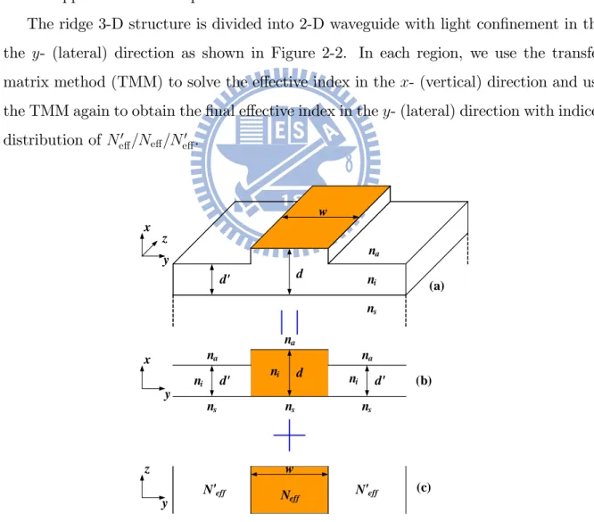
The ridge 3-D structure is divided into 2-D waveguide with light con…nement in the the y- (lateral) direction as shown in Figure 2-2. In each region, we use the transfer matrix method (TMM) to solve the e¤ective index in the x- (vertical) direction and use the TMM again to obtain the …nal e¤ective index in the y- (lateral) direction with indices distribution of N0
e¤=Ne¤=Ne¤0 .
w d' d d d' d' w na ni ns na na na ni ni ni ns ns ns Neff N'eff N'eff x z y x y y z (a) (b) (c)
Figure 2-2: E¤ective Index Method: (a) 3-D ridge waveguide; (b) 2-D equivalence in the x-y plane; (c) 2-D equivalence in the z-y plane.
2.4
Beam Propagation Method
The beam propagation method (BPM) is used to analyze light propagation behavior in the waveguide by solving scalar wave equation along the z- (longitudinal) direction of the waveguide. BPM was derived from a paraxial form of the Helmholtz equation, known as the Fresnel equation. This method is used on waveguide structures with arbitrary cross-section geometries.
In most cases, it is regard as a optical propagation problem starting from the scalar Helmholtz equation. The 3-D scalar wave equation is given by
@2E @x2 + @2E @y2 + @2E @z2 + k 2 n2(x; y; z)E =0, (2.47)
where E is the electric …eld, k is the wave number, and n is the refractive index in the domain of interest.
If the …eld E = (x; y; z)exp( jk0n0z), where is an axially slowly varying function,
n0 is the mean refractive index of the medium, and z is the propagation direction. For a
light beam con…ned in a 2-D cross-sectional waveguide with an index pro…le n(x; z) and paraxial propagating along the z-direction, the scalar wave equation can be modi…ed as
@2 @x2 + @2 @z2 + k 2 0n 2 (x; z) =0, (2.48)
assume = (x; z)exp( jk0n0z)is a wave propagating mainly in the z-direction.
With the slowly varying envelope approximation [15], [16], Eq. (2.48) can be resolved as 2jkn0 @ @z = @2 @x2 + k 2 n2(x; z) n2 0 , (2.49)
then we use a uniform discretization step sizes 4x and 4z, we can derive as 2jk0n0 @ i @z = i+1+ i 1 2 i (4x)2 + k 2 n2(x; z) n2 0 i, (2.50)
where iis the …eld at (u4x; z) and 4x denotes the discretization step in the x-direction. We can repeat these process until the wave reaches the boundary of the domain resulting in …nal …eld distribution. The …nite di¤erence BPM (FDBPM) is more accurate than conventional fast Fourier transform (FFTBPM) in high index contrasts.
There is another method, a linear combination of the “forward-di¤rence” method and the “backward-di¤rence” method, called Crank-Nicolson scheme. By applying the Crank-Nicolson scheme, we obtain
v+1 i 1 + a+i v+1 i + v+1 i+1 = v i 1 ai v i v i+1, (2.51) where a+i = 2 + k02(n 2 i n 2 0)(4x) 2 4jk0n0(4x)2=4z. (2.52) ai = 2 + k02(n 2 i n 2 0)(4x) 2 +4jk0n0(4x)2=4z. (2.53)
the superscripts and subscripts in Eq. (2.51) denote the z- and x-coordinates, respec-tively. For example, vi is the slowly-varying …eld at (i x, v z).
The transparent boundary condition (TBC) [21] is used to deal with the radiation re‡ected back from the computation boundaries. For waveguide structures whose re-fractive indices di¤er greatly from the average rere-fractive index (the reference index), the Padé approximent operator [22] is also implemented in the simulation.
For this research, we utlize the BeamPROP software included in the commerical software package R-soft V.5.1 to simulate the optical propagation characteristics of our designed devices.
Chapter 3
Design of Si-Based Dual ARROW
Power Splitters
3.1
Introduction
ARROW structure was …rst reported in 1986, which utilizes the Fabry-Pérot re‡ection instead of the total internal re‡ection (TIR) as the guiding mechanism. In contrast to the conventional waveguides, the ARROW structures are promising for photonic integrated circuits (PICs) due to their distinctive features: (a) e¤ective single-mode propagation, (b) low loss of e¤ective single mode, (c) large core size suitable for e¢ cient connection to …bers, (d) selective losses depending on the wavelength and on the polarization of the light, (e) large fabrication tolerance for refractive indices and thicknesses of cladding layers between the core and the substrate, and (f) various choice of waveguide materials for each layer [23].
3.2
Characteristics of an ARROW Structure
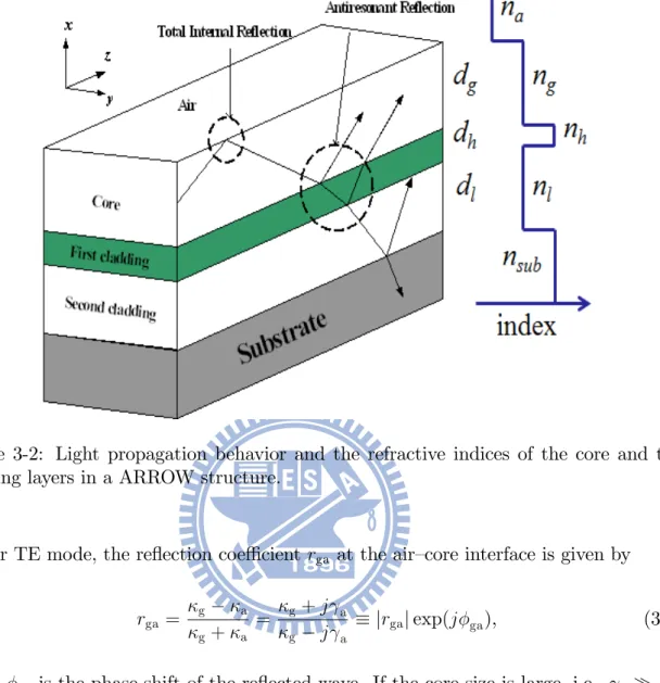
The basic con…guration of a slab ARROW waveguide (na/ng/nh/nl/ns) is shown in Figure
3-1. For an ARROW structure, light is con…ned by antiresonance conditions within the cladding layers and by total internal re‡ection at the air–core interface. The refractive index of the …rst cladding layer is higher than the core and the second cladding layers, as shown in Figures 3-1 and 3-2. The amount of power passing through the interface corresponds to the propagation loss.
In order to achieve high re‡ectivity at the core-cladding interface, both of the …rst and the second cladding thicknesses are designed to satisfy the antiresonance condition to pro-duce the destructive interference within them, which is known as Fabry-Pérot resonance [24]. The re‡ection from the interference within the cladding layers depends strongly upon the polarization of guided light, which is a kind of multiple Fresnel re‡ection.
n
subn
lnh
n
gn
a z xair
Figure 3-1: The cross-section schematic of a slab ARROW waveguide.
In this following, we derive the con…nement condition of the planar ARROW structure from the ray–optical picture, as shown in Figure 3-2. Supposing that a zig-zag beam with a certain incident angle is guided in the core region. The optical …eld decays evanescently in the air region because of the total internal re‡ection at the air-core interface. The transverse propagation constant g in the core region and a in the air region are given
by g = q k2 0n2g 2, (3.1) a = j a, (3.2) a q 2 k2 0n2a, (3.3)
Figure 3-2: Light propagation behavior and the refractive indices of the core and the cladding layers in a ARROW structure.
For TE mode, the re‡ection coe¢ cient rga at the air–core interface is given by
rga = g a g+ a = g + j a g j a jrgaj exp(j ga), (3.4)
where ga is the phase-shift of the re‡ected wave. If the core size is large, i.e., a g,
then ga approaches . The re‡ection coe¢ cient rgh at the interface of the core and the
…rst cladding is given by rgh = g h g+ h jr ghj exp(j gh), (3.5) where h g, so gh approaches .
In order to form a constructive interference in the core layer, the following condition should be satis…ed
if the core size is not large enough, Eq. (3.6) must be modi…ed as
2 gdge=2 ) gdge= , (3.7)
where dge is the e¤ective thickness of the core layer.
Rearranging Eq. (3.6) and applying Snell’s law, we can derive Eq. (3.8) as 2 0 ngcos gdg , (3.8) ) cos h = 1 sin2 h 1 2 = 1 n 2 g n2 h sin2 g 1 2 , (3.9) 1 n 2 g n2 h + 2 0 4n2 hd2g 1 2 , (3.10)
where g and hrespectively represent the ray angle in the core layer and the …rst cladding
layer. From the transmission characteristics of a Fabry-Pérot resonator, high re‡ection of cladding layer exists under the antiresonance condition. The antiresonance condition is de…ned as
2 idi = (2m + 1) , m =0, 1, 2, (3.11)
where i represents the transverse propagation constant in the i cladding layer.
From Eqs. (3.10) and (3.11), the antiresonance conditions of the …rst and the second cladding layers are derived as
dh = 0 4nh 1 n 2 g n2 h + 2 0 4n2 hd2g 1 2 (2P + 1), P = 0, 1, 2, (3.12) dl = 0 4nl 1 n 2 g n2 l + 2 0 4n2 ld2g 1 2 (2Q + 1). Q =0, 1, 2, (3.13)
If the refractive index of the second cladding layer nl and the core layer ng are the same,
Eq. (3.13) can be simpli…ed as
dl
dg
3.3
Design of the Slab ARROW Structure
For single-mode propagation, the core size of the ARROW structure can be large to get better coupling e¢ ciency with the single-mode …ber. In our slab ARROW structure, the refractive indices of the core layer ng, the …rst cladding layer nh, and the second cladding
layer nl are chosen as 1.45, 3.7, and 1.45, respectively. In order to perform the series of
simulations in the following sections, all layer’s material parameters of the slab ARROW structure need to be de…ned. In the slab ARROW structure, we chose silicon dioxide (SiOx ) as the core material and its thickness was designed as 2.0 m. From Eqs. (3.12) and (3.13), we chose P = 0 and Q = 0 for minimum the thicknesses of the …rst and the second cladding layers. Amorphous silicon was chosen as the material of the …rst cladding layer and its thickness was designed as 0.12 m. For fabrication convenience, we chose the same material of the second cladding layer as the core layer, and its thickness must be designed as 1.0 m. The parameters of the slab waveguide are shown in Table 3.1, and the operation wavelength is 1.55 m. Table 3.2 shows the propagation losses of …rst three modes of both TE and TM polarizations.
For reducing the propagation loss of the fundamental mode, we used two antiresonant cavities under the core layer, as shown in Figure 3-3 and Table 3.1. Our fabrication process was chosen (100) p-type silicon as the substrate.
The loss is de…ned as
Loss (dB=cm) = 10 log10 Pout Pin , (3.15) = 10 log10 (E0 e j (1 cm))(E0 e j (1 cm)) E0E0 , = 10 log10e2k0ImfNe ¤g(1 cm), = 20 k0ImfNe¤g(1 cm) log10e, (3.16) where
= k0Ne¤= k0(RefNe¤g + Im fNe¤g) =
2
(RefNe¤g + ImfNe¤g) , (3.17)
is the propagation constant, k0 is the wave number, and Ne¤ is the e¤ective index of
Si Substrate SiOx SiOx a-Si a-Si SiOx n = 3.5 n = 1.45 n = 1.45 n = 3.7 n = 3.7 n = 1.45 dh= 0.12 µm dh= 0.12 µm dl= 1.0 µm dl= 1.0 µm x y z dg= 2.0 µm
Figure 3-3: The cross-section schematic of the slab ARROW structure.
The simulation characteristics of our slab ARROW waveguide are shown in Figures 3-4 and 3-5. In Figure 3-4, when the thickness dg of the core layer reaches about 1.5
m, the propagation loss of the fundamental mode, TE0, would be less than 1 dB/cm.
Therefore, we chose the thickness dg of the core layer as 2.0 m still in the tolerance
range. In Figure 3-5, when the thickness dh of the …rst cladding layer reaches 0.12
m; the propagation loss of the fundamental TE mode would be less than 1 dB/cm. Furthermore, the propagation loss within the ‡at region does not vary much, so it can be seen that this design has a feature of large tolerance.
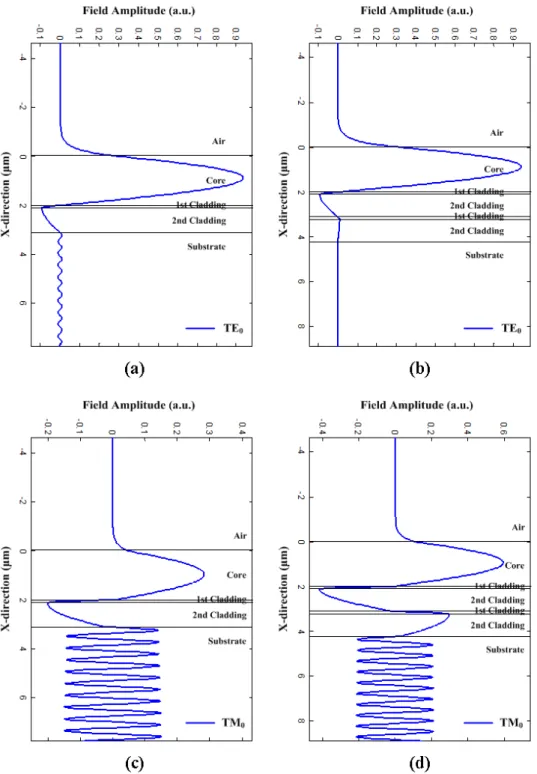
Figures 3-6(a) and (b) show the …eld pro…les of the fundamental TE mode (E-…eld along y-direction) when using one cavity and two cavities. The oscillation behavior of the extension tail of the …eld pro…le in the high index structure in Figure 3-6(b) is less than that in Figure 3-6(a), which means that the loss is reduced when using two antiresonant cavities. Figures 3-6(c) and (d) show the …eld pro…les of the fundamental TM mode (H-…eld along y-direction) when using one cavity and two cavities. The oscillation behavior of the extension tail of the …eld pro…le in the high index structure in Figure 3-6(d) is less than that in Figure 3-6(c), where means that the loss is reduced when using two antiresonant cavities.
1 2 3 4 5 6 7 10-3 10-2 10-1 100 101 102 Core Thickness (µm) P r o p a g a ti o n L o ss (d B /c m ) TE0
Figure 3-4: The propagation losses of the fundamental TE mode versus the core layer thickness dg for the slab ARROW structure with simulation
parame-ter values na=ng=nh=nl=nh=nl=ns = 1.0/1.45/3.7/1.45/3.7/1.45/3.5‚ dh=dl=dh=dl = 0.12/1.0/0.12/1.0 m and = 1.55 m. 0 0.05 0.1 0.15 0.2 0.25 0.3 0.35 0.4 0.45 10-1 100 101 102 103
First Cladding Thickness (µm)
P r o p a g a ti o n L o ss (d B /c m ) TE0
Figure 3-5: The propagation losses of the fundamental TE mode versus the …rst cladding layer thickness dh for the slab ARROW structure with simulation parameter values
na=ng=nh=nl=nh=nl=ns = 1.0/1.45/3.7/1.45/3.7/1.45/3.5‚dg=dl=dh=dl = 2.0/1.0/0.12/1.0
Figure 3-6: The …eld pro…les of the fundamental TE mode: (a) one antiresonant cavity (b) two antiresonant cavities. The …eld pro…les of the fundamental TM mode: (c) one antiresonant cavity, (d) two antiresonant cavities. The parameters are given in Table 3.1.
Table 3.1: The parameters of the slab ARROW structure at the operation wavelength of 1.55 m.
Material Refractive Index Thickness
Superstrate Air na = 1.0
Core Layer SiOx ng = 1.45 dg = 2.0 m
1st Cladding Layer a-Si nh = 3.7 dh = 0.12 m
2nd Cladding Layer SiOx nl = 1.45 dl = 1.0 m
1st Cladding Layer a-Si nh = 3.7 dh = 0.12 m
2nd Cladding Layer SiOx nl = 1.45 dl = 1.0 m
Substrate Silicon ns = 3.5
Table 3.2: The propagation losses of …rst three TE and TM modes when using only one cavity and two cavities. The unit of propagation loss is dB/cm.
TE0 TE1 TE2 TM0 TM1 TM2
One Cavity 10.7 821 994 2832 12128 26404
Two Cavities 0.11 243 122 1341 8983 16873
3.4
Coupling Behavior of Dual ARROW Structures
Coupling behavior of dual ARROW structures was …rst investigated by Baba et al. for using as an uncoupled stacking, and followed by Mann et al. in applying the structure as a directional coupler [1]–[5]. It can be found that we can control the structural symmetry to operate a dual ARROW as a directional coupler or as two decoupled waveguides. Most of the results are accurate only in weakly coupling situations. For dual ARROW structures with leaky modes, the strong coupling between two waveguides must be considered [24]. The following is a review of the method based on the interference of the fundamental even and odd modes [25] and used to analyze the coupling e¢ ciency of a dual ARROW structure, as shown in Figure 3-7.
The …eld distributed in a dual ARROW guided system can be expressed as
E(x; z) = AeEe(x) exp( jk0Nez) + AoEo(x) exp( jk0Noz), (3.18)
H(x; z) = AeHe(x) exp( jk0Nez) + AoHo(x) exp( jk0Noz), (3.19)
where Ae and Ao are the amplitudes of the normalized even and odd modes with e¤ective
Superstrate
Upper Core
Separation Layer
Lower Core
Si Substrate
2 nd Cladding Layer
1 st Cladding Layer
z
x
1 st Cladding Layer
1 st Cladding Layer
1 st Cladding Layer
2 nd Cladding Layer
(magnetic) …elds of even and odd modes, respectively. For TE modes, the power density Sz is Sz(x; z) = 1 2Re[( ~E H ) ^~ az] = 1 2Re[Ey(x; z)Hx(x; z)] = 1 2RefA 2 eEe(x)He(x) + A 2 oEo(x)Ho(x) +AeAo [Ee(x)Ho(x) + Eo(x)He(x)] cos[k0(Ne No)z]g. (3.20)
The even and odd modes are orthonormal with respect to the Poynting power as
P = Z 1 1 Sz(x; z)dx = Pg1 + Pg2 + Pelse = (A2e + A2o) = 1, (3.21) where Pg1(z) = Z g1 Sz(x; z)dx; Pg2(z) = Z g2 Sz(x; z)dx; and Pelse(z) = Z else Sz(x; z)dx, (3.22)
Pg1 is the guided power in the upper core g1, Pg2 is the guided power in the lower core g2, and Pelse represents the remaining power in the region outside cores g1 and g2. Light is launched into the upper core in Figure 3-7 at the reference plane z = 0 such that there is a reference power Pg1 guided in the upper core.
To calculate the coupling e¢ ciency C(z) from the upper core in our structure to the lower core at any z position, we must investigate the power variation Pg2 in the lower
core. The power in the core g1 at a position z is
Pg1(z) = A2e ee+ A 2 o oo+ AeAo( eo+ oe) cos[k0(Ne No)z], (3.23) where ij = 1 2 Z g1 Ej(x)Hi(x)dx, (i; j = e, o). (3.24)
To minimize the uncoupled power Pg2(0) + Pelse(0), the cross product AeAo is released as AeAo = eo + oe [( ee oo)2+ ( eo+ oe)2] 1 2 . (3.25)
Assume that the power is mainly guided inside g1 and g2, then
Pelse(z) Pg2(z), (3.26)
and we can utilize the following approximations:
Pg2(z) Pg1(z) = Pg1(0) Pg1(z)
= 2AeAo( eo+ oe) sin
2 k0(Ne No)
2 z . (3.27)
We can obtain the coupling e¢ ciency based on above equations as
C(z) = Pg2(z) Pg1(0) = Cosin2( cz), (3.28) where Co = 2( eo+ oe)2 ( ee+ oo) [( ee oo)2+ ( eo+ oe)2] 1 2 + ( ee oo)2+ ( eo+ oe)2 , (3.29) c = k0(Ne No) 2 , (3.30)
Co is the maximum coupling e¢ ciency at a length z equal to the coupling length (Lc).
In the case that light is launched into the lower core, the above formulas will also be satis…ed if Pg1 and Pg2 are exchanged with each other.
The size is one of the most important factors in the cost and integration capability for an integrated optical device and a compact device is always attractive, it is desirable to shorten the coupling length and in turn the device length for a coupler. We design our devices based on the theory.
3.5
Design of the Dual ARROW Power Splitters
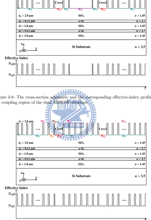
The dual ARROW power splitter include three parts: the input region, the coupling region, and the decoupling region. The basic structure and the corresponding e¤ective-index pro…le obtained by the transfer matrix method (TMM) and the e¤ective e¤ective-index method (EIM) are depicted in Figures 3-8 to 3-9. Along the vertical direction, the structure was chosen as the ARROW structure instead of the conventional structure, and
we used the SiOx as the core material. It can guide lightwaves in a low-index (ng =1.45)
core with a large core size (dg =2.0 m), and their core index and size can be compatible
with a single-mode …ber, which can provide e¢ cient coupling. Moreover, we used the a-Si as the …rst cladding material, because it is commonly used in semiconductor processing and the refractive index is more larger than SiOx, which can minimize the thickness of …rst cladding. Along the lateral direction, some regions in the y-direction were etched to make the structure be the ARROW type to con…ne light in the core, respectively. ARROW-based structure can be remotely coupled because of their nondecaying …eld pro…le inside the intermediate cladding layers. We can use this distinctive features to design our devices.
The width wl1 of the second cladding layer of our dual ARROW structure in the
y-direction was designed as 3.5 m based on the antiresonance conditions. The propagation loss of the fundamental mode, TM0 (E-…eld along y-direction), would be less than 1
dB/cm. The width wh1 of the …rst cladding layer was calculated as 1.24 m. For
fabrication convenience and the guided e¢ ciency enhancement, the depth dx was chosen
as 2.0 m. The real part of Ne¤H was solved as 1.438 for TE polarization and 1.436
for TM polarization by using the Matlab programs, and the real part of Ne¤L was 1.408
for TE polarization and 1.403 for TM polarization. The e¤ective indices of the dual ARROW structure are shown in Table 3.3.
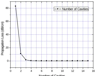
The parameters of the dual ARROW structure are shown in Table 3.4. The prop-agation losses of one cavity to …fteen cavities are shown in Table 3.5, and Figure 3-10 shows the relations between the propagation losses of the fundamental TM mode and the number of cavities.
A dual ARROW structure can operate as a directional coupler or as two decoupled waveguides by controlling the structural symmetry. In order to simplify the structure of our dual ARROW waveguides, we designed the input region as the decoupling region. In the decoupling region, we chose wh2 and wl2 as 0.5 and 4.24 m to reduce the coupling
e¢ ciency by satisfying the antiresonance conditions. In the coupling region, we chose wh3 and wl3 as 0.5 and 19.2 m to enhance the coupling e¢ ciency by satisfying the
resonance conditions. From these simulation results, we used twelve cavities to reduce the propagation loss in the lateral direction.
Si Substrate SiOx SiOx a-Si a-Si SiOx n = 3.5 n = 1.45 n = 1.45 n = 3.7 n = 3.7 n = 1.45 dg= 2.0 µm dh= 0.12 µm dh= 0.12 µm dl= 1.0 µm dl= 1.0 µm x y z Core1 dx= 2.0 µm Wg1 Wl1 Wh1 NeffH NeffL Effective Index y Core2 Wg2 Wl3 Wh3 Wl1 Wl1 Wh1 Wh1 … … Wh3Wh1 Wl1 … …
Figure 3-8: The cross-section schematic and the corresponding e¤ective-index pro…le in the coupling region of the dual ARROW structure.
Si Substrate SiOx SiOx a-Si a-Si SiOx n = 3.5 n = 1.45 n = 1.45 n = 3.7 n = 3.7 n = 1.45 dg= 2.0 µm dh= 0.12 µm dh= 0.12 µm dl= 1.0 µm dl= 1.0 µm x y z Core1 dx= 2.0 µm Wg1 Wl1 Wh1 NeffH NeffL Effective Index y Core2 Wg2 Wl1 Wl1 Wh1 Wh1
…
…
Wl2 Wh2…
…
Figure 3-9: The cross-section schematic and the corresponding e¤ective-index pro…le in the decoupling region of the dual ARROW structure.
Table 3.3: The e¤ective indices of the dual ARROW structure at the operation wave-length of 1.55 m.
TE0 TM0
Ne¤H 1.438 - 1.69 10 8 i 1.436 - 2.46 10 4 i
Ne¤L 1.408 - 3.21 10 7 i 1.403 - 3.81 10 3 i
Table 3.4: The parameters of the dual ARROW power splitters at the operation wave-length of 1.55 m.
ng 1.45 nh 3.7 nl 1.45 ns 1.35
dg ( m) 2.0 dh ( m) 0.12 dl ( m) 1.0 dx ( m) 2.0
wg1, wg2 ( m) 7.0 wh1 ( m) 1.24 wl1 ( m) 3.5
wh2 ( m) 0.5 wl2 ( m) 4.24 wh3 ( m) 0.5 wl3 ( m) 19.2
3.6
Simulation Results for the Dual ARROW Power
Splitters
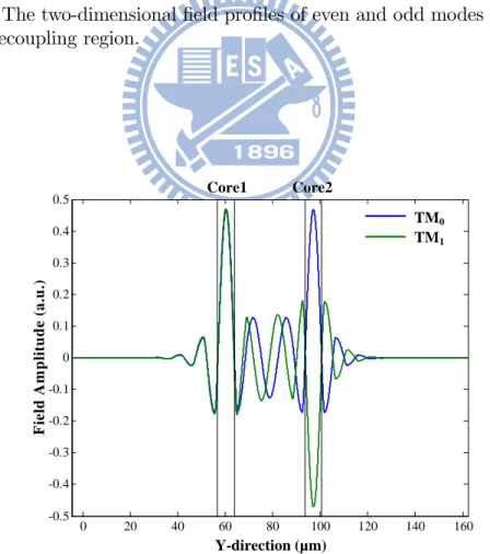
Figure 3-11 shows the two-dimensional …eld pro…les of even and odd modes (E-…eld along y-direction) in the dual ARROW structure for two cores with twelve cavities for TM polarization when the separation width is 30 m in the decoupling region, and the propagation loss is 0.11 dB/cm. Figure 3-12 shows the two-dimensional …eld pro…les of even and odd modes in the dual ARROW structure for TM polarization when the separation width is 30 m in the coupling region. In the coupling region, our designed ARROW structure can be remotely coupled because of their nondecaying …eld pro…le inside the intermediate cladding. The propagation losses of the …rst ten modes of TM polarization in the decoupling region and the coupling region are shown in Tables 3.6 and 3.7, respectively. For the dual ARROW structure, when the beam is launched into
Table 3.5: The relations between the propagation losses of the fundamental TM mode and the number of cavities. The unit of prapagation loss is dB/cm.
Number of Cavities 1 2 3 4 5 6 7 8
Propagation Loss 82.9 11.0 1.57 0.31 0.14 0.12 0.11 0.11
Number of Cavities 9 10 11 12 13 14 15
0 2 4 6 8 10 12 14 16 0 20 40 60 80 P ropagat ion Loss (dB /cm ) Number of Cavities Number of Cavities
Figure 3-10: The relations between the propagation losses of the fundamental TM mode and the number of cavities.
either core, only two modes, TM0 and TM1, are dominantly excited. So the coupling
theory in Section 3.4 can be used to design the power splitters. The coupling length can be obtained by
Lc =
2(Nei Noi)
; (3.31)
when only TM0 and TM1 modes are dominant, where is the operation wavelength and
Nei; Noi(i = E or M for TE polarization or TM polarization) are the real part of e¤ective
indices of even and odd modes, respectively.
The calculated coupling length is 4300 m and the separation width is 30 m. In our research, we designed the length of the coupling region at z = Lc / 2 to equally split the
power of incoming signals into two output ports with an equal power. When the beam is launched into the left core and the right core, the beam propagation method (BPM) simulation results are shown in Figures 3-13 and 3-14. The coupling length is almost the same as the value calculated by using the Matlab programs.
The total length of the dual ARROW power splitter was designed as 14000 m with 4000- m, 2150- m (Lc/2), and 7850- m lengths of the input region, the coupling region,
0 50 100 150 -0.6 -0.4 -0.2 0 0.2 0.4 0.6 TM0 TM1 Core1 Core2 Y-direction (µm) F ie ld A m p li tu d e (a .u .)
Figure 3-11: The two-dimensional …eld pro…les of even and odd modes for TM polariza-tion in the decoupling region.
0 20 40 60 80 100 120 140 160 -0.5 -0.4 -0.3 -0.2 -0.1 0 0.1 0.2 0.3 0.4 0.5 TM0 TM1 Core1 Core2 Y-direction (µm) F ie ld A m p li tu d e (a .u .)
Figure 3-12: The two-dimensional …eld pro…les of even and odd modes for TM polariza-tion in the coupling region.
Table 3.6: The propagation losses of the …rst ten modes for TM polarization in the decoupling region. Mode Loss (dB/cm) TM0 0.109 TM1 0.109 TM2 7.7 TM3 8.6 TM4 5.5 TM5 29.7 TM6 30.6 TM7 45.4 TM8 63.7 TM9 48.6
Table 3.7: The propagation losses of the …rst ten modes for TM polarization in the coupling region. Mode Loss (dB/cm) TM0 0.109 TM1 0.108 TM2 7.1 TM3 8.4 TM4 8.7 TM5 29.0 TM6 32.3 TM7 18.1 TM8 65.3 TM9 58.6
Y (µm) 100 - 0 100 Z ( µ m ) 3000 -0 3000 6000 9000
Monitor Value (a.u.) 0.0 0.5 1.0 Pathway, Monitor: 1, Power 2, Power
Figure 3-13: The BPM simulation result of the dual ARROW power splitter for separation width of 30 m and the length of the coupling region of 2150 m (Lc/2) when the beam
launched into the left core.
Y (µm) 100 - 0 100 Z ( µ m ) 3000 -0 3000 6000 9000
Monitor Value (a.u.) 0.0 0.5 1.0 Pathway, Monitor: 1, Power 2, Power
Figure 3-14: The BPM simulation result of the dual ARROW power splitter for separation width of 30 m and the length of the coupling region of 2150 m (Lc/2) when the beam
and the decoupling region, respectively. The beam propagation method (BPM) included in the commercial software package R-soft V.5.1 was used to simulate our designed dual ARROW power splitters by launching a power into the left core or the right core. For verifying the coupling characteristics and the performances of the power splitters, we also designed and fabricated …ve di¤erent lengths of the coupling region as 1950, 2050, 2150, 2250, and 2350 m as examples.
Chapter 4
Fabrication of Si-Based Dual
ARROW Power Splitters
4.1
Introduction
In this chapter, we will introduce the fabrication of Si-based dual ARROW powers split-ters. Our vertical ARROW structure includes three SiOx layers (one is the core and two are the second claddings) and two amorphous silicon layers (the …rst cladding) in between. We used the Oxford PECVD (Plasma-Enhanced Chemical Vapor Deposition) system (STS multiplex cluster system) to deposit SiOx layers, and the HDPCVD (High Density Plasma Chemical Vapor Deposition) system to deposit amorphous silicon layers. In addition, we used the thermal coater system to deposit aluminum to be our hard mask. After depositing all layers, the lithography and etching process were proceeded. Finally, we used the wet bench to remove the residual aluminum layer and the in-line scanning electron microscopy (in-line SEM) to inspect the fabrication process. Figure 4-1 shows the fabrication processes of the dual ARROW power splitters and the fabrications were processed in the National Nano Device Laboratories (NDL) and in Nano Facility Center at National Chiao Tung University. The detailed fabrication parameters are discussed in the following sections.
Flow
Chart
Si Substrate SiOx SiOx a-Si a-Si SiOx 0.12 µm 0.12 µm 1.0 µm 1.0 µm 4.0 µm(1) Deposit five layers by HDPCVD and PECVD. Si Substrate SiOx SiOx a-Si a-Si SiOx 0.12 µm 0.12 µm 1.0 µm 1.0 µm 4.0 µm A l 0.3 µm (2) Deposit Al layer by Thermal Coater. Si Substrate SiOx SiOx a-Si a-Si SiOx 0.12 µm 0.12 µm 1.0 µm 1.0 µm 4.0 µm A l 0.3 µm Photoresist Si Substrate SiOx SiOx a-Si a-Si SiOx 0.12 µm 0.12 µm 1.0 µm 1.0 µm 4.0 µm A l 0.3 µm Si Substrate SiOx SiOx a-Si a-Si SiOx 0.12 µm 0.12 µm 1.0 µm 1.0 µm 4.0 µm Si Substrate SiOx SiOx a-Si a-Si SiOx 0.12 µm 0.12 µm 1.0 µm 1.0 µm 2.0 µm Si Substrate SiOx SiOx a-Si a-Si SiOx 0.12 µm 0.12 µm 1.0 µm 1.0 µm 2.0 µm (3) Spin coat negative
photoresist by Track.
(4) Pattern by Track and E-beam.
(5) Etch Al layer by Metal Etcher.
(6) Etch Oxide layer by Metal Etcher.
(7) Remove residual Al layer by Wet Bench.
4.2
Deposition
Basically, RCA cleaning is necessary for a wafer to eliminate organic, inorganic attach-ment, and other contaminants. After RCA cleaning, we used the Chamber-B of the Oxford PECVD system to deposit SiOx …lms for the core and the second cladding lay-ers. The PECVD system can deposit thick …lms with lower stress, and the deposition rate is faster than a horizontal furnace system. Moreover, the PECVD system produces oxide …lms with high conformality and low viscosity at a low deposition temperature.
The designed thickness of the second cladding layer is 1 m, and the thickness of the core layer is 2 m. The deposition parameters for 1- m SiOx are listed in Table 4.1.
Table 4.1: Deposition parameters for 1- m SiOx :
Time (sec) 965 RF Power (50kHz) 40 TEOS (sccm) 50 O2 (sccm) 300 Pressure (mTorr) 500 Temperature ( C) 350
Then we used the HDPCVD system to deposit the amorphous silicon …lm (the …rst cladding layer) with a thickness of 0.120 m. The chemical reaction is
SiH4 ! Si + 2H2. (4.1)
By try and error, the better parameters were found to deposit thin …lms with high refractive index, low stress and good uniformity. The deposition parameters for 0.120
m a-Si are listed in Table 4.2. Here, we repeated three times in the steps 1 to 3. Table 4.2: Deposition parameters for 0.120- m amorphous silicon.
Steps 1 2 3 Time (sec) 180 1 600 ICP Power (W) 0 45 45 Pressure (mTorr) 200 200 200 Ar (sccm) 50 50 50 H2(sccm) 800 800 800 SiH4 (sccm) 50 50 50 Temperature ( C) 200 200 200
are shown in Figure 4-2 and Table 4.3. The average thickness of the core layer was deposited as 2.07 m. The thicknesses and the indices of each layer were measured by using “N&K analyzer 1500”, it is a popular thin …lm measurement system based on the patented “N&K method” [27]. The method can use to calculate the thickness and the refractive index of thin …lms by utilizing Forouhi and Bloomer dispersion equations based on quantum mechanics.
Then we used the thermal coater system to deposit the aluminum layer with 3000 Å thickness as a hard mask. Since we expected to transfer the image from the photoresist (P.R.) to the underneath …lm without any critical dimension loss, therefore, a perfect etching pro…le is favored.
1
2 3
4
5
Figure 4-2: The locations of measuring …ve points on a 6-inch Si wafer.
Table 4.3: The thicknesses and the refractive indices of the …ve points of cladding layers
at = 1.55 m.
Material SiOx a-Si
Thickness / Refractive Index d ( m) n d ( m) n Location 1 1.13 1.455 0.123 3.85 Location 2 1.10 1.457 0.118 3.82 Location 3 1.11 1.454 0.120 3.85 Location 4 1.07 1.455 0.117 3.81 Location 5 1.13 1.457 0.119 3.84 Average 1.11 1.456 0.119 3.83
4.3
Lithography
Figure 4-3 shows the layout pattern of the dual ARROW power splitter which includes three parts: the input region, the coupling region, and the decoupling region, which was designed by R-soft and L-edit software. After completing the deposition processing steps, we used the “Clean Track MK-8” system for the lithography process. If the wafer was bended too much, the machine arm of the exposure system could not grab it. Therefore, before coating P.R., we used the stress measuring instrument to measure the radius of curvature of the wafer. The lithography procedures are described as follows: a. Spin Coating and Soft Baking
On the wafer surface, we added the HMDS, (CH3)3SiNHSi(CH3)3, for enhancing the
adhesion between the wafer and P.R.. The temperature is 90 C and the baking time is 60 seconds. After cooling the wafer, the negative photoresist was applied. Initially, the speed of spin coating should be slow for the P.R. spread uniformly on the wafer surface. The spin coating speed was set as 500 rpm for 10 seconds. Then it ramps to the …nal speed of 5000 rpm for 45 seconds. The thickness of negative P.R. is 3800 Å.
b. Hot-plate Unit
The step was used to remove the solvent of P.R. and to enhance the adhesion between the Al and P.R. layers. The temperature of the step is 90 C and the baking time is 90 seconds.
c. Exposure, Development and Hard Baking
The dual ARROW power splitters were patterned by the “Leica E-beam” (Leica weprint 200) with exposing dosage 4.5 C=cm2. We used the “Clean Track MK-8” for exposure and development. After developing, we used hard bake to harden the resin within the P.R. and stop the reaction between the developer and P.R. layers. The tem-perature of the step is 120 C and the baking time is 90 seconds. Finally, we used the in-line SEM to inspect the fabrication results.
Decoupling Region 7850 µm Coupling Region 2150 µm (Lc/2) Input Region 4000 µm
Figure 4-3: Layout diagram of the dual ARROW power splitter.
4.4
Etching Process and AEI (after etching
inspec-tion)
After completing after-develope-inspection (ADI), we used the metal etcher, “ILD-4100”, for etching aluminum of 3000 Å and SiOx of 20000 Å. The etching recipes are shown in Tables 4.4 and 4.5. The etching time for aluminum of 3000 Å is about 38 seconds and for SiOx of 20000 Å is about 600 seconds.
Table 4.4: The recipe for etching aluminum 3000 Å by using metal etcher, “ILD-4100”.
Steps 1 2 Time (sec) 3 35 RF Power (W) 1000 1000 Bias Power(W) 100 100 Pressure (mTorr) 5 5 Cl2 (sccm) 85 100 N2(sccm) 15 0
Load Value Auto Auto Tune Value 4050 4050
In the recipes, CHF3 was used to produce polymers and CF4 was used to produce
Table 4.5: The recipe for etching SiOx 20000 Å by using metal etcher, “ILD-4100”. Step 1 Time (sec) 600 RF Power (W) 1000 Bias Power (W) 75 Pressure (mTorr) 4 CF4(sccm) 20 CHF3 (sccm) 20
Load Value Auto Tune Value 3250
etching process, we used the wet-bench system to remove the residual aluminum …lm on the wafer with the chemical solution of H2SO4 : H2O2 =3 : 1 at 130 C for 10 minutes.
Then we used the P-10 surface pro…ler to meausre the depth and the in-line SEM to measure the width. After etching inspection (AEI) images were photographed by the in-line SEM.
Figures 4-4 (a) to (c) show the AEI topview SEM images of the coupling region and the decoupling region of the dual ARROW power splitters, and the average etching depth of the trench is 1.98 m. Coupling Region Decoupling Region (a) (b) (c)
Figure 4-4: The AEI topview SEM images of (a) the dual ARROW power splitter, (b) the coupling region, and (c) the decoupling region.
Chapter 5
Characterization and Discussion
5.1
The Setup of the Optical Measurement System
After accomplishing all of the fabrication process, we used the lensed …bers coupled with the waveguide input and output in the optical measurement system to perform the experiments for characterizing the performance for our designed devices at the operation wavelength of 1.55 m, and the setup is illustrated in Figures 5-1 and 5-2.
The optical measurment instruments contain:
(1) The 1.55- m diode laser: It can be used to generate the light of of 1.55 m. (2) Lensed …bers: They are used to provide a convenient way to improve coupling between an optical …ber and a waveguide device.
(3) Optical microscope (OM): It assists the alignment of the …bers with the input and output ports of the waveguide.
(4) Infrared (IR) charge-coupled device (CCD) camera: It can view the light spot at of 1.55 m, and we put a 20X lens in front of IR camera to focus the light spot.
(5) TV monitor: It can display the light spot images from the IR camera to facilitate observation and photography.
(6) Photodetector: It is used to detect and measure the optical power. (7) Power meter: It shows the power intensity.
First, we aligned the lensed …ber with the input port of the dual ARROW waveguide. Next, we put the IR camera on the output port of the dual ARROW waveguide, and move the position of the input lensed …ber near the input port of the waveguide. At this time, we tuned the x, y, and z positions of the stage and the IR camera until two clear
Optical Breadboard Optical Microscope Waveguide Sample holder 1.55-µm Diode Laser stage Lensed Fiber Fiber chuck holder Fiber chuck Y Z X IR camera TV Monitor 20 X lens Fiber Polarizing Controller
Figure 5-1: The optical measurement setup for the alignment of the input lensed …ber with the IR camera.
Photodetector Optical Breadboard Optical Microscope Waveguide Sample holder Lensed Fiber Fiber chuck holder stage Lensed Fiber Fiber chuck holder stage
Fiber chuck Fiber chuck
Power Meter X Y Z Z Y X 1.55-µm Diode Laser Fiber Polarizing Controller
Figure 5-2: The optical measurement setup with photodetector for the power measure-ment.
light spot images on TV monitor were obtained, as shown in Figure 5-3. The stringent requirements for end-face ‡atness and alignment accuracy at the input and output of the waveguides are necessary. After we aligned the lensed …ber, we removed the IR camera and put the output lensed …ber near to the output port of the devices, as shown in Figure 5-2, and tuned the x, y, and z positions of the input and output ports stages until the power meter read a maximum value. Finally, the output power was detected by the photodetector, and the power intensity were recorded and displayed on the power meter.
The Light Spot
30 µm
Figure 5-3: The IR camera image of the light spot from the output port of the dual ARROW power splitter with a separation width of 30 m.
5.2
Cut-back Method for Propagation Loss of the
Dual ARROW Power Splitters
For verifying the performances of the power splitters with a coupling length Lc of 4300
m, we designed …ve di¤erent lengths power splitters, 1950, 2050, 2150 (Lc/2), 2250, and
2350 m, and we launched a power only into the left core or only into the right core to measure the output power. In the experiment, guided waves were excited and we used
the cut-back method to measure the propagation losses of the waveguides. The method is often used for measuring the total attenuation of a waveguide device and has the advantage that a relatively accurate measurement is possible with a simple con…guration, but it is a destructive method and information about mode-order dependence of losses can not be obtained. The propagation losses of the transmittances with di¤erent lengths of the device can be obtained as
=
10 log P2
P1 L2 L1
(dB/cm), (5.1)
where P1, P2 and L1, L2 are the transmittances and the lengths before and after cutting,
respectively. Here, we de…ne the P1 and P2 are the sum of Pcore1 and Pcore2 with di¤erent
lengths, where Pcore1 is the output power of core 1 by launching a power only into the
left core or only into the right core and Pcore2 is the output power of core 2 for launching
a power only into the left core or only into the right core. The power in decibel relative to 1 mW is de…ned as
P (dBm) = 10 log Pcore1+ Pcore2
1 mW . (5.2)
We measured …ve samples to analyze the characteristics of the power splitters. The relations between the values of the normalized output power and the propagation lengths of the samples 1, 2, 3, 4, and 5 by launching a power only into the left core and only into the right core are shown in Figures 5-4 to 5-8. Then, the values of propagation losses from the slope of the linear …tting line were obtained. Tables 5.1 to 5.5 show the propagation losses of the samples 1, 2, 3, 4, and 5 by linear …tting in Figures 5-4 to 5-8. The results are quite consistant.
Table 5.1: The propagation loss measurement results of …ve samples for launching a power (a) only into the left core and (b) only into the right core, respectively. The length of the coupling region is 1950 m.
(a) Sample Number 1 2 3 4 5 Propagation Loss (dB/cm) 1.92 2.89 4.99 2.26 2.42 (b) Sample Number 1 2 3 4 5