IEI E TRANSACTIONS ON MICROWAVE THEORY AND TECHNIQUES, VOL. 41, NO. 8, AUGUST 1993 1391
Analysis of the Effects of a Resistively Coated Upper
:Dielectric Layer on the Propagation Characteristics
of Hybrid Modes in a Waveguide-Shielded
Microstrip Using the Method of Lines
Shyh-Jong Chung, Member, IEEE, and Lin-Kun Wu, Member, IEEE
4bsfracf- In this paper, propagation characteristics of even- symmetric hybrid modes in a waveguide-shielded microstrip in the presence of a resistively coated dielectric layer afixed to the top cover of the housing is analyzed with the method of lines. The resistive boundary condition is employed to model the resistive film. A shielded microstrip line having a unity strip-width-to-substrate-thickness ratio (i.e., w / h l = 1) placed
om top of a 0.635-mm-thick alumina substrate is considered. Based on a lOh1 x 7hl reference housing, four different housing at rangements are obtained by varying the structural parameters of the resistively coated dielectric layer. Results obtained indicate that the effects of both the housing walls and the resistively coated upper dielectric layer on the dominant (quasi-TEM) mode are insignificant and may be ignored when frequency is above
1C GHz. For the higher order modes, resistive film appears to bt, transparent when film resistance is greater than about 1 ks1,
it behaves as a good conductor when film resistance is much snialler than 100 0, and in between it results in nonlinear (and e\ en oscillatory) higher order modal behaviors. Apparently, due
to the increasing field concentration inside the upper dielectric
(as suggested by the increasing for a given mode, both the maximum attenuation and the film resistance needed to achieve it increase with frequency and dielectric constant of the upper dielectric layer.
I. INTRODUCTION
ICROSTRIPS are open structures that tend to radi- ate as the operating frequency increases. However, in p .actice, hybrid and monolithic microwave and millimeter- mave integrated circuits are enclosed in a metal package tc protect the circuit from the environment and to provide electrical isolation between different parts of the subsystem. When an electrically small enclosure is used, a broader single- n ode (i.e., quasi-TEM) operating frequency range is obtained. however, approaching package walls results in more field to
h: present in the air region of the shielded microstrip circuit M hich modifies the dominant microstrip mode characteristics o
F
uniform lines and discontinuities [1]-[4].Proximity effects on the dominant mode characteristic can
h: minimized by the use of an electrically large enclosure Manuscript received May 4, 1992; revised January 22, 1993. This work was slipported by the National Science Council of the Republic of China under (,rant NSC 81-0404-E-009-529.
The authors are with the Institute of Communication Engineering, National Chiao Tung University, 1001 Ta Hsueh Rd, Hsinchu, Taiwan 30050.
IEEE Log Number 9210204.
y t
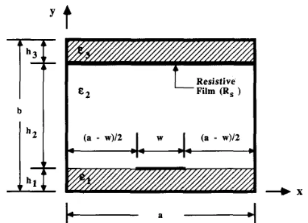
Fig. 1. Cross-sectional view of the waveguide-shielded uniform microstr p line with a resistively coated dielectric layer affixed to the top cover.
which, however, can support several modes. When the frc- quency approaches or is above the cutoff frequency for highcr order mode propagation, erratic circuit behaviors in the fonn of package resonance or enhanced parasitic coupling among circuit elements have been reported in [2] and [5]-[8]. As was
pointed out in [2], shielding effects due to the onset of higher order modes are more important than shielding effects due to wall proximity. This observation is particularly important in view of the constantly increasing circuit complexity ard operating frequency in the development of MIC's [9], [lo].
As a consequence, aside from being able to predict the
shielding effects of the higher order modes, it is perhaps even more desirable and important to devise efficient ways for suppressing them.
Recently, a less expensive and more reliable altemath'e to the conventional methods for the suppression of package resonances (a summary of these traditional methods can be found in [ l l ] ) was proposed [12]. In this latter approach, a dielectric layer coated with a resistive film is fixed under the lid of a package containing a large (M)MIC, using the same processes of fixing the microstrip circuit to the bottom of the package. Since the field associated with the dominant (quasi- TEM) mode is confined mainly in the immediate surroundings of the strip conductor, it would not interact strongly with, 0018-9480/93$03.00 0 1993 IEEE
I 94 IEEE TRANSACTIONS ON MICROWAVE THEORY AND TECHNIQUES, VOL. 41, NO. 8. AUGUST 1593
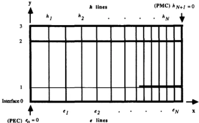
Fig. 2. Illustration of lines used in the nonequidistant discretization scheme over the half of the shielded microstrip structure to be analyzed.
a i d is thus not attenuated much by, the resistive film. On ttie other hand, higher order modes, with their fields spread ovrer the entire cross section of the package, will in general
e cperience some loss due to the current flow on the surface of
t t le resistive coating. Package resonance and parasitic coupling
a nong circuit elements may then be suppressed.
While damping performance of a resistively coated dielec- tric layer on the lowest order box mode of a rectangular cavity
v as considered in [12], the frequency-dependent complex
p -0pagation constants of shielded microstrips modes in a
v aveguide-type of housing, which includes a resistively coated tl (electric layer affixed to its top cover, are analyzed in this piper. A cross-sectional view of the structure to be analyzed
i c shown in Fig. 1. The method of lines [13], which is
it iailable to us for other applications, is used in this analysis. I‘3r simplicity, we consider only the cases where the strip conductor is placed symmetrically with respect to the two
5 i dewalls. Furthermore, since the dominant quasi-TEM mode i k even-symmetric with respect to the plane of symmetry at
J = a/2, and for the purpose of demonstrating the efficacy of
tt e resistively coated dielectric layer for attenuating higher (I-der modes, only the even modes that are characterized
h~ having a zero tangential magnetic field at the plane of s~rmmetry are considered in this paper. The odd mode behavior
c in be analyzed in a similar fashion by replacing the magnetic
uall at z = a/2 with a corresponding electric yall. The present method differs from the method of lines doc- unented in [13] in the use of Senior’s resistive boundary condition [14] to account for the presence of the resistive fiIm. Therefore, only the major steps used in the traditional n ethod of lines together with the additional resistive boundary a gorithm are summarized in Section. 11. Some numerical tamples obtained for four different housing arrangements 2 e then presented in Section 111. Conclusions are presented
ir Section IV.
thus reduces the problem to a two-dimensional one. For the even modes characteristics to be considered in this paper, the problem space can be halved by introducing a magnetic wall at the plane of z = n/2. The resultant structure is shown in Fig. 2, with discretization lines along the y-axis for the z
components of the electric and magnetic fields, e, and h,. Similarly, an electric wall can be placed at z = u / 2 for determining the odd-mode characteristics.
Following the procedures described in [ 131, a transformation procedure is obtained
where, for p = 0,1,2,3,
and
are the transformed tangential fields at the upper ( p = m ) and lower ( p = m - 1) interface planes of the m t h dielectric layer
shown in Fig. 2, and
JL,
y ,
andz
are matrices determined by the properties of the layer involved.After applying the boundary conditions at the perfect elec- tric conductors present at interface 0 and 3 (Le., ICo =
E 3
= 0), use of (1) yieldsand
with
(5) where sub-superscripts
“+”
and “-” signify, respectively, thatE l m ’ s are taken “above” and “below” the corresponding m h interface.
Next, the resistive film at interface 2 is assumed to he characterized by having a finite conductivity (T and a thickneis
11. FORMULATION
A cross-sectional view of the structure to be analyzed is
shown in Fig. 1. For the shielded microstrip considered here, t t e structure is assumed to be symmetrical along the z-axis
CHI JNG AND WU: EFFECTS OF RESISTIVELY COATED UPPER DIELECTRIC LAYER ON PROPAGATION 139.’ TABLE I
SUMMARY OF THE A~DITIONAL STRUCTURAL PARAMETERS USED FOR EACH OF THE FOUR HOUSINGS EXAMINED I N THIS PAPER
WA WB
wc
WD 9.7 1 NIA 2.27- which is much smaller than the skin depth, such that it may be modeled as an infinitesimally thin resistive film with a constant surface resistance R, = (l/a~) R [14]. It is noted th it the resistive film becomes an infinitesimally thin perfect electric conductor when R, = 0 R, and it is nonexistent a i e n R, becomes infinite. When crossing such a resistive sheet, the tangential electric fields are continuous while the c( rresponding tangential magnetic fields are discontinuous, ard the two sets of tangential field components must satisfy
th c following resistive boundary condition [14]:
f i x E2 =
R,h
x (H2+ - H 2 - ) (6) or, in the transform domain,Tnen from (4) and (7) we get (3)’
W 2 - = - Y t
E,
H ith
(7)
(9) Finally, by substituting (8) into (l), the following relationship i: obtained:
a,+
=-yplC1
(10)where
From (3),
(lo),
and the boundary condition at interface 1, an inhomogeneous matrix equation is obtainedZJ1
=E
l
(12)\qhere J1 represents the transformed current distribution along interface 1. By transforming back to the spatial domain,
i nd recognizing that nonzero conduction currents and zero
t engential electric fields exist over the strip portion of the interface 1, a reduced matrix equation can be obtained
ZrJ;
= 0 (13)tvhere the current vector
L J z J
contains only nonzero J , and J , over the strip [13]. The desired modal dispersion characteristics of the structure can then be obtained by simply enforcing the condition of
iet(2’) = 0.
111. RESULTS AND DISCUSSIONS
Results to be presented in this section are all derived using the following nonequidistant discretization scheme [ 151. For the discretization scheme shown in Fig. 2, e, and h, are set to zero for the respective e,-line along the electric wall at 5 = 0, and the h,-line along the magnetic wall at z = a / ; . Among the total of Ne,-line and Nh,-line used, Nu, e,- line and Nu - 1 h,-line are placed across the strip with a
constant subinterval between any two adjacent e,- and h,- lines. For lines between the strip edge and the sidewall, this subinterval increases as a geometrical series with quotient q of successive subintervals being a constant [ 151. Furthermore, the edge condition is satisfied by positioning the edge of the infinitely long strip half-way between the two adjacent ei
-
and h,-lines [13].
In this paper, four different housing arrangements are used. For convenience, they are designated as housing WA, WB, WC, and WD. For the structural geometry shown in Fig. 1, the following common parameters are used in these housings: w =
h l = 0.635 mm, ~1 = 9 . 7 ~ ~ (Le., alumina substrate), ~2 =
E , , h~ = 5h1, and a = 10hl. Additional structural parameters
are summarized in Table I. It is noted that with a’s and b’s chosen here, the dominant (quasi-TEM) mode is expected to experience only a minimal degree of proximity effect at lower frequencies within housings WB and WC [4]. Therefore, additional structural parameters associated with housings WA and WD will be used to demonstrate the effects of resistively
coated dielectric substrate on the propagation Characteristics of higher order modes.
A. Shielded Microstrip with Single Dielectric Substrate As a numerical check, Fig. 3 compares the dominant mode
dispersion curves calculated for: 1) the shielded microstrip contained in housing WB using two discretization schemes with the present method, and 2) the corresponding unshielded microstrip using the closed-form expressions given in [ 161 (which are considered to be very accurate for unshielded microstrips). Excellent convergence has been achieved in the present method as the results obtained by the two discreti- zation schemes having (Nu = 15, N = 32, and q = 1.1) and
(N,,, = 30, N = 51, and q = 1.1) are almost identical through- out the entire frequency range. Although not shown here, this also holds when q = 1 and 1.2 are used with the
(N,,, = 15, N = 32) discretization scheme. Given these, the
discretization scheme with
(Nw
= 15, N = 32, and q = 1.1) is used to obtain the results to be presented in the followhg. Furthermore, Fig. 3 shows that while all three sets of data areIEEE TRANSACTIONS ON MICROWAVE THEORY AND TECHNIQUES, VOL. 41, NO. 8, AUGUST 19j3 1 : 96 b. 0 8 I This Research (Nw = 15) This Research (Nw = 30) 0
" .
-.
..
-
, -.
.
.
0 10 20 30 40 50 Frequency (GHz)F ~ g . 3. Comparison of the effective dielectric constant of the dominant mode ~ ( r s u s frequency calculated for: 1) the shielded case with housing WB using t h - present method, and 2) the unshielded case using the closed-form formula
01 [16]. Two discretization schemes with ( N , = 15, N = 32, q = 1.1) and
( . I u , = 30, N = 5 1 , q = 1.1) are used in the present method.
a .e predicted by the present method for the shielded case at
I( lwer frequencies; similar observations were also made in [ 171
fc ir the case of a waveguide-shielded microstrip having finite n etallization thickness. In summary, Fig. 3 reveals that: 1)
c'invergent and accurate results can be obtained by the present n,ethod, and 2 ) proximity effect of the approaching walls on the dominant mode dispersion characteristics can be ignored for frequency above 15 GHz.
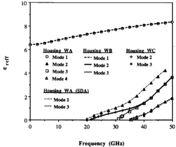
b. Shielded Microstrip with Additional Upper Dielectric Layer
Next, effects of the additional upper dielectric layer (with illfinite R,) on the modal dispersion behaviors are illustrated
i i i Fig. 4 for housings
W A
andWB.
Fig. 4 also shows thetl ispersion data obtained by the spectral-domain approach
(SDA)
for Modes 2 and 3 of housingWA,
which clearlyd :monstrates the accuracy of the present method in analyzing higher order modal behaviors. In addition, for future reference purposes, dispersion curves for the first two higher order niodes (Le., Modes 2 and 3) associated with housing
W C
are;I.SO illustrated in Fig. 4.
As
can be seen, for housingsW A
andWB,
dominant riiode (i.e., Mode 1) dispersion curves are almost the same. This should be expected since the dominant modal fields c mcentrate mainly near the strip conductor such that the effect due to the additional upper dielectric layer in housingW A
i:, insignificant. On the other hand, since higher order modal fields (Le., Modes 2, 3, etc.) extend over the entire cross
sxtion of the housing, modal structures are modified by the I: resence of the upper (non-air) dielectric layer. Specifically, I )r the results to be discussed next, it is noted that below about 3 5 GHz, two propagating higher order modes are supported by housing
W A
(and WD, for which the dispersion curves are not s iown here to prevent further cluttering the drawing) and only (.'ne each in housingsW B
andW C
(which, in the absence I. f the upper dielectric, have quite similar modal dispersion1- ehaviors). In the following, the influences of the resistive
2 - Mode
.
--
Mode 30 10 20 30 40 50
Frequency (GHz)
Fig. 4. Effective dielectric constant versus frequency calculated for housings WA (with infinite Rs), WB, and WC by the present method (N, = 15, N = 32, and q = 1.1). Data obtained by the spectral-domain approach (SDA) for Modes 2 and 3 of housing WA are also shown for
comparison. h h L 21 al L W - 1
d
L W E -3- c( -4- Mode 2 - 1 0 1 2 3 4 5 Log@ 1Fig. 5. Complex effectlve dielectric constant versus log ( R , ) calculated jor Modes 2 and 3 of housing WA. (Frequency = 35 GHz, N,. = 15, N = 2 2, and q = 1.1.)
coating on the modal dispersion behaviors of Modes 2 and 3
of housing
W A
will be investigated further.C. Shielded Microstrip with a Resistively Coated Upper Dielectric Layer
Fig. 5 displays the variations of the complex ~ ~v e r s s ~ f f
log(R,) for Modes 2 and 3 of housing
W A
at 35 GHz; the complex for which det(2') = 0 is satisfied is determined using the Muller's method, where c r P f f found for a given R, is used as the initial guess for the next R, when 12,decreases from infinity to zero. Although not shown here, t i e real part of of the dominant mode remains essentially t ?e same as shown in Fig. 4, while only negligibly small values of the imaginary part of (and attenuation constant) are detected, for all resistance values considered.
~~ ~~
CHI NG AND W U : EFFECTS OF RESISTIVELY COATED UPPER DIELECTRIC LAYER ON PROPAGATION
‘;or Mode 3, when log(R,)
>
3.5, the effects of the film arerat ier insignificant such that Re{ assumes essentially the same value as that shown in Fig. 4 (Le., infinite R,) while
In:{~,,ff} M 0. However, when log(R,)
<
1.5, Mode 3 of ho ising WA has an Re{Ereff} M 0.967 (and Im{&,,ff} M 0),wbich is the same as that of the Mode 2 of housing WC shown in Fig. 4. When log(R,) decreases from 3.5 to 1.5,
thr magnitude of Im{&,,ff} increases first, and reaches its mLximum value when log(R,) M 2.7 (Le., R, M 500 0) be- foi e decreasing again to zero. These observations indicate that M )de 3 of housing WA reduces to the propagating Mode 2 of housing WC as zero R, is approached.
In contrast to Mode 3, computations are made only for lc ;(&)
>
2.373 (Le., R,>
236R)
for Mode 2. Since the ze -0 and pole of det [ Z ” ] are so close to each other, an accurate determination of the zero for Mode 2 becomes extremely dificult when log(R,)<
2.54. This is reflected by the fact t h i t for the data shown in Fig. 5, computations are actually performed for more than 1000 R, values (each requiring a n t mber of iterative steps) over the range of 2.54>
log(R,)>
2.373 @e., 350
R
>
R,>
236 R)! Due to this numerical di €ficulty, we are not able to proceed computation any further. For the data obtained and shown in Fig. 5, it is found that both R ?{&,,.ff} and Im{q.,ff} of Mode 2 remain fairly constantfl r large value of R,. When log(R,) decreases below 3
( e., R,
<
1 kR), magnitude of the Im{&,,ff} increases nionotonically while Re{e,,ff} drops rapidly before reachinga minimum value of 0.353, when log(R,) = 2.54 (i.e.,
I t , = 350
fl),
it increases afterward. In terms of complexp’ opagation constant, the phase exhibits similar oscillatory bchavior as Re{Ereff} while attenuation constant shows the
si me monotonic behavior as Im{E,,E}. When computation n a s finally terminated at log(R,) = 2.373, the attenuation c I Instant has reached an extremely large value of 78.4 dB/cm.
I. 3r comparison, the maximum attenuation suffered by Mode 3
i c only about 6 dB/cm at log(R,) x 3 [see Fig. 7(b)].
The above data indicate that resistive film appears to be tiansparent to the modal fields when R,
>
1 kfl, it is quite 11)ssy (mainly due to absorption) for R, in the 100’s R range, and it behaves as a good conductor when R,<<
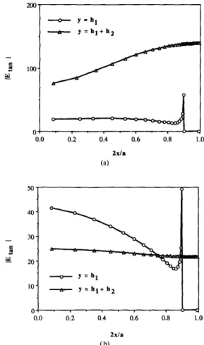
100 R. To examine why Mode 2 suffers more attenuation than Mode 3, magnitudes of the total tangential electric field (IEtan( in .jrbitrary unit) computed for Modes 2 and 3 along interfaces 1i 7 = h l ) and 2 (y = hl
+
h2) of housing WA with infinite /is are shown in Figs. 6(a) and (b), respectively. It is notedr
iat since normalization of the field strength over different r lodes is difficult, ratio of the field strength obtained at the two iiterfaces for each mode is used to infer the loss mechanism. Figs. 6(a) and (b) reveals that Mode 2 has a much largerI atio of the (average) field strength along interface 2 to that of
interface 1 than Mode 3. Since lEtanl has to vanish at the top Tvall, the above comparison also points out that Mode 2 has a larger portion of its energy distributed in the upper dielectric legion. As a consequence, Mode 2 has a higher than dode 3 when the resistive film is absent (see Fig. 4) and, more importantly, it shall lose more energy (by means of tbsorption) to the resistive film (see Fig. 5). The generally ,mailer and relatively uniform field distribution found along
0.0 0.2 0.4 0.6 0.8 1 .o 2xla (a) 1397 I 40 - 30
-
- a B - 20- -2- Y = h l l0 0 l - z L - A 0.0 0.2 0.4 0.6 0.8 1 .o Zala ( b)Fig. 6. Distributions of the magnitude of the total tangential electric fields along interfaces 1 and 2 for: (a) Mode 2, and (b) Mode 3 of housing W A with infinite R,. (Frequency = 35 GHz, Nw = 15, N = 32, and q = 1.1.) interface 2 for Mode 3 indicates that only a small amount of its energy is distributed inside the upper dielectric (at 35 GHz). This should also explain why, as shown in Fig. 4, its ~~~~f
is so similar to that of the Mode 2 of housing WB which hds no upper dielectric.
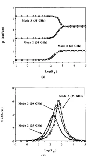
In Figs. 7(a) and (b), variations of the real and imaginary parts of the propagation constant IC, (Le., IC, = /3
-
j a = ( m k o ) as a function of log(R,) are depicted for: 1) Mode 2 at 25 GHz, 2) Mode 2 at 30 GHz, and 3 ) Mode 3 at 35 GHz. Since attenuation constant for Mode 2 at 35 GHzreaches a very large value of 78 dB/cm when computation was terminated at log(R,) = 2.373, it is not displayed here
for clarity. Fig. 7(a) shows that the effects of the resistive film on
0’s
are insignificant in all three cases considered when log(R,) is greater than 3 (i.e., R,>
1 kR). This is followed by a transition region over a range of 3>
log(R,)
>
1.5 in which decreasingp’s
are observed. As zcro R, is approached,P’S
obtained for the Mode 2 of housingWA at 25 GHz and 30 GHz and Mode 3 at 35 GHz redu:e,
respectively, to that of the Mode 2 in housing WC (specif- ically, from data shown in Fig. 4, we have: = 0.373, or /3 = 3.196 rad/cm, at 25 GHz; &,(.ff = 0.633,
IEEE TRANSACTIONS ON MICROWAVE THEORY AND TECHNIQUES, VOL. 41, NO. X, AUGUST 19‘*3 I 6 5 Mode 2 (25 GHz) _ I . -1 0 1 2 3 4 5 Mode 3 (35 GHz) Mode 2 (30 GHz) - 1 0 1 2 3 4 5
f ‘ g. 7. (a) Phase constant and (b) attenuation constant versus log(%) c; lculated for Mode 2 at 25 and 30 GHz, and Mode 3 at 35 GHz, of housing MA. ( N w = 15, N = 32, and q = 1.1.)
( 1 - /3 = 5.192 rad/cm, at 30 GHz; and = 0.967, or ii = 7.207 rad/cm, at 35 GHz). These results indicate that hybrid mode dispersion behavior inside housing WC can be rtcovered from that of the housing WA with diminishing (but n mzero) film resistance. This may thus be viewed as a validity cieck on the accuracy of the higher order mode data (in particular, the effects of the resistive film) obtained by the present method.
Similar to the behavior of Im{Ereff} shown in Fig. 5 for Mode 3 at 35 GHz, all three sets of data shown in I-ig. 7(b) reveal that a’s increase first as log(R,) decreases fiom 5 , and a maximum value is reached in each case before (1 :creasing again as log( R,) decreases further. Furthermore, c imparison between the maximum attenuations suffered by the Mode 2 at 25 and 30 GHz indicates, that the maximum
ii .tenuation, and the film resistance needed to achieve it, iiicreases with increasing frequency. As suggested by the iiicreasing found in Fig. 4, this again attributed to the increasing field/energy distribution inside the upper dielectric layer as frequency increases.
Finally, the effect of the material used for the upper layer
i:. demonstrated in Fig. 8. In this case, (Y versus log(R,),
cdculated at 30 GHz for the Mode 2 of housing WD, is
-1 0 1 2 3 4 5
L d R s )
Fig. 8. Attenuation constant versus log(&) calculated for Mode 2 of how- ings WA (i.e., ~~3 = 9.7) and WD (i.e., ~~3 = 2.2). (Frequency = 30 GHz, N , = 1 5 , N = 32, and q = 1.1.)
compared to the corresponding data obtained for the Mode 2 of housing WA. As shown in Table I, the only difference betwet n
the two is that € 3 = 9 . 7 ~ ~ and 2 . 2 ~ ~ are used with housings
WA and WD, respectively. With the remaining structural
parameters being the same, smaller ~3 used in housing WD apparently results in weaker field strength inside its upper dielectric layer. As a consequence, Fig. 8 shows the smalllx attenuation constants are obtained for housing WD.
IV. CONCLUSIONS
In this paper, use of a resistively coated dielectric layer affixed to the top wall of the housing for the suppression of higher order shielded microstrip modes is investigated. For simplicity, only even modes are considered; nonetheless, the formulation presented in this paper can be extended to the analysis of odd-mode characteristics simply by replacing the magnetic wall used here with the corresponding electric waJ. It is found that for the specific housings considered, prou- imity effects of the housing walls on the dominant mode char- acteristics may be ignored for frequency exceeding 15 GHz. Since the dominant modal fields concentrate mainly in the immediate surroundings of the strip conductor, the abo1.e statement holds both with and without the presence of the resistively coated dielectric layer. On the other hand, as highx order modal fields extend over the entire cross section of the housing, interactions with the coated upper dielectric layer are expected.
For large R, @e., greater than about 1 kfl), film is almost transparent to the modal fields such that
/3
remains essentially the same as, while a increases only slightly from, the case Jfinfinite R,. For R, in the order of 100’s of ohms, film b e c o m s absorptive, and significant interaction between the crossing fields and the film occurs. Nonlinear, and even oscillatory, modal propagation characteristics are found as R, varies in this range. In general, except for the oscillatory behavior found in Mode 2 of housing WA at 35 GHz,
/3
shifts monotonically toward that of the case of zero R,; it stays at that value whimR, continues to decrease toward 0
fl.
On the other hand, a continues to increase until a maximum value is reached, andCHI ING AND WU: EFFECTS OF RESISTIVELY COATED UPPER DIELECTRIC LAYER ON PROPAGATION 1395
thcn decreases to zero when R, approaches zero. For a given ml de (e.g., Mode 2 of housings WA and WD), increases as frequency andlor dielectric constant of the material used in tht upper layer increases. It may serve as an indication of increasing field concentration inside the upper dielectric. As such, the maximum attenuation, and film resistance needed to achieve it, increase with frequency and dielectric constant of thc upper dielectric layer. For R,
<<
100 0, film behaves as a good conductor with low conductor loss.Finally, Mode 2 (at 25 and 30 GHz) and Mode 3 (at 35 GHz) of housing WA are found to transform smoothly to
the. corresponding Mode 2 of housing WC as film resistance
de sreases from infinity toward (but never reached) zero. Since t hc modal characteristics associated with housing WC (see Fi:. 4) are obtained in the absence of the resistively coated upper dielectric layer, these results may be considered as an independent check on the validity of the use of the present mdhod for the determination of the effects of the resistively coated dielectric layer on the hybrid modal behaviors.
ACKNOWLEDGMENT
The authors are grateful to the reviewers for their critical cc mments which improved this paper.
[6] A. Hill and V.K. Tripathi, “An efficient algorithm for the three- dimensional analysis of passive microstrip components and disconti. nuities for microwave and millimeter-wave integrated circuits,” IEEE Trans. Microwave Theory Tech., vol. 39, pp. 83-91, Jan. 1991.
[7] A. Sabban and K.C. Gupta, “Effects of packages on parasitic, coupling among microstrip discontinuities in MMICs,” Inr. J . Microwavo Millimeter- Wave Computer-Aided Eng., vol. 1, no. 4, pp. 403-410. 1991.
[8] J. Moore and H. Ling, “Characterization of a 90’ microstrip bend with arbitrary miter via the time-domain finite difference method,” IEEI’ Trans. Microwave Theory Tech., vol. 38, pp. 405-410, Apr. 1990.
191 Special issue on Multifunctions MMIC’s and Their System Applications,
IEEE Trans. Microwave Theory Tech., vol. 38, Sept. 1990.
[lo] Special section on RF Integrated Electronics, Proc. IEEE, vol. 79, Mar. 1991.
[ l l ] R. K. Hoffman, Handbook ofMicrowave Integrated Circuits. Nomood,
MA: Artech House, 1987, pp. 399-400.
[12] D. F. Williams, “Damping of the resonant modes of a rectangular metal package,” IEEE Trans. Mcrowave Theory Tech., vol. 37, pp. 253-2561,
Jan. 1989.
1131 R. Pregla and W. Pascher, “The method of lines,” in Numerical Techniques for Microwave and Millimeter-Wave Passive Structure:,
T. Itoh, Ed.
[14] T. B. A. Senior, “Approximate boundary conditions,” IEEE Trans. An- tennas Propagut., vol. 29, pp. 826-829, Sept. 1981.
[15] H. Diestel and S.B . Worm, “Analysis of hybrid field problems bv the method of lines with nonequidistant discretization,” IEEE Tran:;. Microwave Theory Tech., vol. 32, pp. 633-638, June 1984.
[ 161 M. Kobayashi, “A dispersion formula satisfying recent requiremenls in microstrip CAD,” IEEE Trans. Microwave Theory Tech., vol. 3%
[17] F. J. Schmuckle and R. Pregla, “The method of lines for the ana1ys.s of ulanar waveeuides with finite metallization thickness,” IEEE Tranv.
New York: Wiley, 1989, ch. 6.
pp. 1246-1250, Aug. 1988.
- r
Microwave Theiry Tech., vol. 39, pp. 107-111, Jan. 1991
REFERENCES 111 I 21 I31 141 51
L. P. Dunleavy and P. B. Katehi, “A generalized method for analyzing shielded thin microstrip discontinuities,” IEEE Trans. Microwave Theory Tech., vol. 36, pp. 1758-1766, Dec. 1988.
-
, “Shielding effects in microstrip discontinuities,” IEEE Trans. Microwave Theory Tech., vol. 36, pp. 1767-1773, Dec. 1988.S. March, “Microstrip packaging: Watch the last step,” Mlcrowuves,
pp. 83-94, Dec. 1981.
L. K. Wu and Y. C. Chang, “Characterization of the shielding effects on the frequency-dependent effective dielectric constant of a waveguide- shielded microstrip using the finite-difference time-domain method,”
IEEE Trans. Microwave Theory Tech., vol. 39, pp. 1688-1693, Oct.
1991.
R. H. Jansen and L. Wiemer, “Full-wave theory based development of
mm-wave circuit models for microstrip open end, gap, step, and tee,” in IEEE M i T S Int. Microwave Symp. Dig., 1989, p. 779-782.
i
in electromagnetics.
Shyh-Jong Chung (M’92) was born in Taipei, Taiwan, Republic of China, on January 18, 1962. He received the B.S.E.E. degree in 1984, and the Ph.D. degree in 1988, both from National Taiwan University, Taipei, Taiwan.
Since 1988, he has been with the Department of Communication Engineering, National Chiao Tung University, Hsinchu, Taiwan, R.O.C., where he is currently an Associate Professor. His areis of interests include waveguide discontinuities, EMI, wave propagation, and numerical techniquzs