I314 IEEE JOURNAL OF SOLID-STATE CIRCUITS, VOL. 29, NO. 11, NOVEMBER 1994
A 10-b
125-MHz CMOS Digital-to-Analog
Converter (DAC) with Threshold-Voltage
Compensated Current Sources
Shu-Yuan
Chin and Chung-Yu WuAbstract-This paper describes a 10-b high-speed COMS DAC fabricated by 0.8-pm double-poly double-metal CMOS technol- ogy. In the DAC, a new current source called the threshold- voltage compensated current source is used in the two-stage cur- rent array to reduce the linearity error caused by inevitable cur- rent variations of the current sources. In the two-stage weighted current array, only 32 master and 32 slave unit current sources are required. Thus silicon area and stray capacitance can be reduced significantly. Experimental results show that a conver- sion rate of 125 MHz is achievable with differential and integral linearity errors of 0.21 LSB and 0.23 LSB, respectively. The power consumption is 150 mW for a single 5-V power supply. The ridfall time is 3 ns and the full-scale settling time to *1/2 LSB is within 8 ns. The chip area is 1.8 mm x 1.0 mm.
I. INTRODUCTION
IGH-SPEED and high-resolution digital-to-analog con-
H
verters (DAC’s) are key components in scanning graphic systems, computer systems, digital TV, high-definition TV, etc. In these systems, the DAC’s with the resolution higher than 8-b and the operating frequency higher than 65 MHz are required. Realizing such DAC’s in COMS has many advan- tages such as low cost, low power consumption, and good U 0 compatibility with both COMS and TTL circuitry. Moreover, CMOS DAC’s have good compatibility with memories and digital processing systems so that they can be integrated on the same chip.Recently, many high-speed CMOS DAC’s have been de- signed using either weighted current array [1]-[4] or current cell matrix [5]-[7]. These current-switching DAC’s allow fast and accurate settling. However, parameter gradients over a wafer and mutual mismatches of current sources result in large variations on the performance of the fabricated DAC’s. Thus the resolution of these DAC’s is often restricted to 8 b. In [8]-[ 101 special layout arrangement and switching sequence are used to improve the linearity of current matrix so that 10-b resolution is achievable. Most of them [9]-[lo] require careful combinations on the interconnection netwrok of 2” - 1
equally sized MOS current sources for a n-b DAC. Thus both wiring and switching complexity and silicon area are increased significantly for a high-bit video DAC. Large silicon area
also makes the mismatching and threshold variations among the current sources worse and worse. In [ l l ] , another 10-b DAC is proposed which uses resister strings with a wide- band output buffer to drive low-resistance load. Although the passive components of the DAC can achieve a good linearity, the design of the wide-band, high-drive, and high- speed output buffer is often difficult to be achieved. This limits the maximum operating frequency of the DAC.
In this paper, a 10-b 125-MHz DAC fabricated in 0.8-pm double-poly double-metal CMOS process is designed by using new current sources called the threshold-voltage compensated current sources. These threshold-voltage compensated current soruces use the local matching technique to overcome the problem of linearity errors caused by threshold-voltage gradi- ents over a wafer. Special switching sequence is not necessary since these current sources do not need global matching. The structure of the proposed DAC is based upon the weighted current sources that can drive a 50-0 doubly terminated cable
without an output buffer. In this structure, 5-b master stage and 5-b slave stage current arrays can be adopted to reduce the number of current sources as well as the amount of parasitic capacitances. Thus only 32 master and 32 slave current sources are required for the 10-b DAC with two-stage current array structure. Because the current level of each master current source is 32 times of that of the slave current source, it is much more difficult to maintain the linearity error of each master current source to be within f 1 / 2 LSB over a wafer. However, the tight matching requirement among the current sources in the master stage can be achieved by the threshold- voltage compensated current sources. No special decoding of the digital input data is used. Thus complicated decoding circuitry can be avoided.
In Section 11, circuit structures, operation principles, and design considerations of two-stage current array DAC and threshold-voltage compensated current sources are presented and analyzed. In Section 111, the measurement results are described. Section IV gives conclusions.
11. CHIP DESIGN
Manuscript received June 21, 1993; revised May 31, 1994. This work was supported by the National Science Council, ROC, under the contract NSC82- The authors are with Integrated Circuits and Systems Laboratory, De- partment of Electronics Engineering and Institute of Electronics, National
A . Two-Stage Architecture
0416-E-009-212. The circuit diagram of a conventional weighted-current-
sources are switched between output load and dummy load, according to the value of the input bits which controls the DAC is shown in Fig. 1 [2], Weighted cascade current
Chiao-Tung University, Hsinchu 300, Taiwan, Republic of China. IEEE Log Number 9404998.
CHIN AND WU: A 10-b 125-MHz CMOS DiGITAL-TQ-ANALOG CONVERTER (DAC) WITH THRESHOLD-VOLTAGE COMPENSATED CURRENT SOURCES 1375
Fig. 1. Conventional weighted-current-source DAC architecture.
To Coax To D u m m y Load I I
Iy In
1Y IYBY
YB
,Pa
54it slave current anay
Fig. 3. Conventional switched current source. *5-bitmostgaurentanay
Fig. 2. The block diagram of the two-stage DAC.
output voltages of the drivers to drive the source-coupled current switches. The switch circuit can keep a constant current flowing at the coupled source node and thus fast settling of output can be achieved. The configuration of Fig. 1 requires
n binary weighted current sources for a n-b DAC. Taking the binary-weighted size of the current sources into account, the total equivalent unit current source number is 2” - 1. To increase the matching accuracy, a special wiring method or switching sequence is also required [2]-[ll]. Thus both wiring complexity and silicon area are increased significantly for a high-resolution video D/A conversion. For example, 1023 equivalent unit current sources are required for a 10- b resolution. Large silicon area also makes the inevitable mismatches among the current sources more serious.
Fig. 2 shows the block diagram of a 10-b two-stage current array DAC. In this approach, a primary or master current array is used for the 5 MSB’s, whereas a secondary or slave current array is used for the 5 LSB’s. In this structure, only 32 master and 32 slave equivalent unit current sources are required for a 10-b DAC. The unit current of each master (slave) current array is the same and denoted as
I M ( I L ) .
The binary-weighted number of unit current sources are connected together to form the binary-weighted current source for each bit. One of the master current source is used to drive the overall slave current array which further partitions the master current into the slave binary-weighted bit currents with the unit currentIL
.
The above master-slave current array configuration is usu- ally used in the design of high-speed bipolar DAC’s with 8-b
or higher resolution. It greatly reduces the number of current sources and thus simplifies the connection among these current sources and makes more efficient use of the chip area [3]-[4]. The amount of stray capacitance at the common source node is small and the recovery time of the voltage at this node during the switching transition can be reduced to achieve a fast conversion. However, it is much more difficult to maintain the linearity accuracy of each master current source to be within f 1 / 2 LSB since the current level in each master current source is 32 times of that in the corresponding slave current source. This problem is not severe in bipolar IC’s since the bipolar device parameter variations are more tolerable than that of CMOS. That is why this configuration is often used to realize a high-resolution video DAC in bipolar process. Even though this configuration is also used to realize CMOS video DAC 151-[8], the slave current array is not more than 3 b. Since the threshold-voltage compensated current sources can achieve good linearity over the wafer, they are used in the two 5-b stage current arrays to realize 10-b video CMOS DIA conversion.
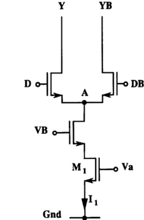
B. Threshold- Voltage Compensated Current Sources
Fig. 3 shows a conventional switched current source. If the Early effect is neglected, the source current 11 can be expressed as:
where p n is the surface mobility, CO is the channel oxide capacitance per unit area, W ( L ) is the channel width(length),
1376 IEEE JOURNAL OF SOLID-STATE CIRCUITS, VOL. 29. NO. 11, NOVEMBER 1994
Y
YB
0 wd
Gnd
-
1
VR1
Fig. 4. Switched current source with threshold-voltage compensation
and Vth is the MOS threshold voltage. In the conventional video DAC with higher than 8-b resolution, a large number of current sources and large chip area are required. The total current is several mA. In this case, the current sources could be hundreds of micrometers apart on the chip and thus the variation of the threshold voltages could be as large as 80 mV
due to the oxide thinning effect [ 2 ] .
The threshold-voltage compensated current source shown in Fig. 4 is proposed to reduce the linearity error caused by the threshold-voltage variations over a wafer. In this circuit, the cascode structure is also used to increase the output impedance of the current source and thus suppress the current variations due to the voltage fluctuations across the current source. Neglecting the Early effect, the source current I2 can
be written as: W2 L2 1 2 = K-(Va - Vthg)' where AV = Va - VR1
-
Vth,In this case, the source current is varied with the difference of Vth, and Vth, rather than Vthz. As long as the transistors
MZ and M, are locally matched, Vth, - Vthz and the current 1 2 is independent of the threshold voltages. Thus the undesirable current variations of the current sources can be reduced significantly. Even if the threshold-voltage mismatch exists, the variation of Vth, - Vthz is still much smaller than
VR1, so that the variation of 1 2 is also very small.
I s o u 1 nu
-
5 5 0 0 . O N-
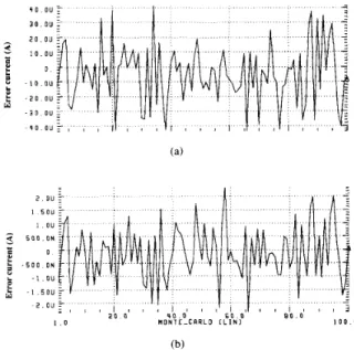
0 - 5 0 0 ON L - 1 . o u - 1 . 5 0 u e (b) Fig. 5 .current sources, (b) current sources with threshold-voltage compensation. SPICE Monte-Carlo simulation results for (a) conventional weighted
A V in ( 2 ) is dependent upon the value of I,, which is
generated by the nonideal current source Mp. Thus AV can be expressed as a function of I,. Using the expression, ( 2 ) can
be rewritten as
As seen from (3), VR1 should be as high as possible and I,
should be as small as possible to reduce the variation of 1 2
due to I,. The W / L ratio of the transistor Mp should be very small and the bias VR2 should be very high to let I ,
<<
1 2 .Thus the variation of I , causes only a small change of 1 2 . In order to keep the variation of I , as small as possible, all of the PMOS transistors (Mps) in each 5-b current array should be locally matched.
SPICE Monte-Carlo simulation results for both conventional current sources and new current sources with threshold-voltage compensation are shown in Fig. 5. It can be seen from Fig. 5 that the proposed new current source circuits can reduce the current variations from &40 FA to f 2 pA when the threshold voltage variation of NMOS devices is within f O . l V and that of PMOS devices is within A20 mV with a Gaussian distribution. Thus this new circuit can achieve 20 times better matching than the conventional current sources.
C. Two-Stage Weighted-Current-Source DAC
Using the two-stage current array configuration and threshold-voltage compensated current sources, the weighted- current-source DAC can be designed as shown in Fig. 6. Note that the LSB current array is connected in cascode to the first current source of the MSB current array. Although the switched current sources in the LSB current array do not use the cascode structure of Fig. 4, they are actually cascoded with
CHIN AND WU: A 10-b 125-MHz CMOS DiGITAL-TO-ANALOG CONVERTER (DAC) WITH THRESHOLD-VOLTAGE COMPENSATED CURRENT SOURCES 1317
Fig. 6. Two-stage weighted-current-source DAC with threshold-voltage compensated current sources.
the first current source in the MSB current array and have a high output impedance as the cascode structure of Fig. 4.
Two methods can be used to obtain a fast settling time. First, the stray capacitance at the common source node of the differential current switches should be kept small to shorten the recovery time of the voltage at the common source node of the differential current switches during transition. This can be easily achieved in this two-stage current array DAC since the two-stage structure requires only 32 master and 32 slave equivalent unit current sources for a 10-b resolution. Secondly, the differential current switches can not be tumed off simultaneously to prevent from large glitch energy which causes long time period to charge the common source node of the differential current switches and discharge the output node of the DAC. If the differential current switches are tumed off simultaneously, the common source node of the differential current switches will be rapidly discharged toward ground and the output node of the DAC will be charged toward power supply voltage. Thus in the following operation, a very long time is required to recharge the common source node of the differential current switches and discharge the output node of the DAC to their optimum operation points. This increases the settling time of the DAC.
To reduce the glitch energy and increase the settling speed, all input digital signals must be input at the same time. The cross point of rising/falling waveforms in the input drivers is also very important. If the cross point of rising/falling
(b)
Fig. 7.
input driver with high logic-threshold,
(a) The circuit; (b) the SPICE simulated output waveforms of the
waveforms in the input driver is high enough, the differential current switches will not tum off at the same time. In this design, the logic threshold voltages of input drivers must be designed to be higher than 4 V to overlap the output waveforms at higher voltage. Thus the time period when the differential current switches are both tumed off can be eliminated and that when both switches are heavily tumed on can be strictly reduced.
In this DAC, a three-MOS inverter as shown in Fig. 7(a) is used as the input driver to increase the logic threshold and
generate overlapped output waveforms shown in Fig. 7(b). The SPICE simulated output waveforms of input drivers show that the risinglfalling cross voltage is higher than 4 V.
D.
chip zmp'ementutionSince the total output current as high as 15- to 25-mA is required to drive the total output load of 10- to 20-pF and achieve fast settling, the line voltage drop along the power
1378
Fig 8 Symmetrical layout conlipration of e ~ c h 5 h i i i i r e n t m r i \
( a ) i h )
Fig. 9.
current source: (a) 4-cell unit: Ih) 5-crll u n l t .
Different layout arrangenicnt of the dc\ir.c.\ .\fi and \ I , i n each
supply line and ground line could be large enough to cause
a gradient error. Therefore. large width of power supply line and ground line is required to reduce the voltage drop. In each 5-b current array, symmetrical layout configuration shown in
Fig. 8 is used to reduce the linearity error caused by the undesirable current variations of the 32 unit current sources. To reduce the noise caused by digital circuitry. analog power lines and digital power lines are both separated. The substrate of digital circuitry is biased by the analog power supply rather than the digital power supply to prevent the digital noise from passing through the substrate and coupling to the analog circuitry.
Two kinds of layout methods for the devices -117 and
Afr in each threshold-voltage compensated current source are
tested in this chip. Fig. 9(a) shows a 4-cell unit layout of the current source. In this topology. the transistor .U' is separated into three pieces which are put together with the threshold- voltage compensated transistor illr to form a compact square. Similarly, Fig. 9(b) shows a 5-cell unit layout of the threshold- voltage compensated current source. In this topology. the transistor M2 is separated into four pieces which are put
around the threshold-voltage compensated transistor 121, to form a directional-symmetric layout.
In order to obtain a better matching among each threshold- voltage compensated current source of Fig. 4. all the transis- tors except Mp are put together in layout to form a11 unit. All
the transistors Mps in the current array are also pui together in
layout to achieve a good local match. Each source current ( I ( , ) of Mp is locally generated and delivered to each threshold- voltage compensated current source.
111. EXPERIMENTAL RESLLTS
Fig. 10 shows the chip photograph of two new DAC's. The chips were fabricated in 0.8-pm double-poly double- metal CMOS technology. The DAC located on the upper part of the chip adopts the threshold-voltage compensated current sources with 4-cell unit layout whereas the D A C located on the lower part of the chip adopts the threshold- voltage compensated current sources with 5-cell unit layout.
I F t t J O l K Y A L OF SOLII)-STATt CIRCIIIT5 L O L 29. N O 1 1 . NOVEMBER 1993
- unit I layout
-
unit layout -Fig. I O . Photograph of the DAC's
0 5-call unit 0 4cell unit a a c
-
10:
n5
0 0.25 0 . 5 1 2 4 8 1 6Dlfferentlal and Integral Nonlinearity (LSB)
Fig I I . o l layout method\.
The nonlinearity histogram of the proposed DAC's with two kinds
TABLE I
L > I F F F R L W U . AND INTE.GKAL 1.IUE.\KI1 Y DlSTRlBllTlON OF T W O
KINDS OF LAYOCT M t 7 H O D S FOR EACH C U R R E N T SOURCE
Linearity Error 4-Cell Unit(%) 5-Cell Unit(%)
< 1/2 LSE3 28.6 21.4
< 1 LSB 82.1 67.9
i 2 LSB 93.9 89.3
The fabricated DAC's are measured with 20-pF output load (including the bonding pad loading) in parallel with a 50-R doubly terminated cable. A 25-0 resistor is used at the dummy output. The reference voltages I 7 X I . L7R2 and VR3 are set to
1.5 V. 4.2 V, and 2.6 V, respectively. Forty dies have been tested and the nonlinearity histogram of the proposed DAC's with two kinds of layout methods i s shown in Fig. 1 1 . The yield is shown in Table I. It is obvious that the DAC with the threshold-voltage compensated current sources of 4-cell
CHIN AND WU: A 10-b 125-MHz CMOS DIGITAL-TO-ANALOG CONVERTER (DAC) WITH THRESHOLD-VOLTAGE COMPENSATED CURRENT SOURCES 1319 -0.3 -0.4 -0.5
-
I
Fig.-
s
I
Fig. --
0.40
.
5
'
1
0.20.31
0.1 0 -0.1 -0.21I
I
I
' 1 ' 1 . 1 '
' I ' ' I '
' 1 ' 4
0.3""i
:::I
, , , ,,I
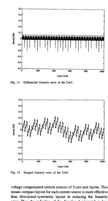
200 400 Mx) 800 loo0 4 . 5 Input CodeIntegral linearity error of the DAC. 13.
voltage compensated current sources of 5-cell unit layout. This means compact layout for each current source is more effective than directional-symmetric layout in reducing the linearity error. Thus the reduction of the directional mismatch is less important than that of the mismatch due to separate distance. The measurement results shown in Fig. 12 to 15 are done for the DAC which adopts threshold-voltage compensated current sources with 4-cell unit layout since it has a better linearity than another one. Being seen from Fig. 12 and 13, the differential linearity error of 0.21 LSB and the integral linearity error of 0.23 LSB can be attained. Thus the fabricated DAC has 11-b accuracy. Fig. 14 shows the full-scale transition and the zooming on rising and falling edges. It can be seen that the 10-90% rise/fall time is 3 ns and the full-scale settling time to f 1 / 2 LSB is within 8 ns. They are almost independent of the riselfall times of the digital input signals. The maximum glitch energy (the transition between 01 11 1 1 1 1 1 1 and lOOOOOO000) shown in Fig. 15 is 40 ps.V. Fig. 16 shows the measured output spectrum of the DAC with an input frequency of 3.9
(C)
Fig. 14.
operation; (b) zooming on the rising edge: (c) zooming on the falling edge. Full-scale transitions of the fabricated DAC in (a) full-swing
TABLE I1 CHARACTERISTICS OF THE DAC
Resolution 10 bits
Differential Nonlinearity 0.21 LSB Settling Time (f1/2 LSB)
Rise/Fall time (1 0-9096)
Supply Voltage 5v
Integral Nonlinearity 0.23 LSE Conversion rate 125 MS/S < 8 ns
3 ns
Glitch Energy 40 psV
Power Dissipation 150 mWatts Process
Chip Size (without pads)
0.8um CMOS 1 . 8 m x 1 .Omm
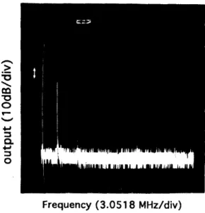
MHz at 125 MHz conversion rate. Further reduction could be realized by using glitchless techniques reported in the literature [9]. The overall signal-to-noise ratio and distortion is obviously dominated by the first and fourth harmonic distortion at 56 dB below signal level. The chip area (without pads) is 1.8 mm
x 1.0 mm. The power consumption is 150 mW. The major characteristics of the fabricated DAC are concluded in Table
II.
1380 IEEE JOURNAL OF SOLID-STATE CIRCUITS, VOL. 29, NO. 11, NOVEMBER 1994
Fig. 15. Photograph of the measured glitch energy of the DAC.
Frequency
(3.051
8 MHz/div)
Fig. 16. The measured output spectrum of the DAC with an input frequency of 3.9 MHz at 125 MHz conversion rate.
IV. CONCLUSION
A 10-b video CMOS DAC has been successfully designed and tested in a 0.8-bm double-poly double-metal CMOS process. Using two-stage current array structure, only 32 master and 32 slave unit current sources are required for a 10-
b resolution. The tight matching requirement of the two-stage current array DAC is achieved by adopting the threshold- voltage compensated current sources. In this D A C , the chip area, wiring complexity, and parasitic capacitance can be reduced significantly whereas 10-b resolution and 125-MHz conversion rate can be readily obtained.
The threshold-voltage compensated current source proposed in this work can also be applied in many other IC design to reduce the inevitable threshold-voltage variations over a wafer. These applications will be addressed in the future.
ACKNOWLEDGMENT
The authors wish to thank Tien-Yu Wu and Yen-Hui Wang for their kind help in the DAC measurement.
REFERENCES
[ 11 Kuang K. Chi et al., “A CMOS triple 100-MbitIs video D/A converter with shift register and color map,” IEEE J. Solid-Srate Circuits, pp.
989-995, Dec. 1986.
121 A. Cremonesi. F. Maloberti, and G. Polito, “A 100-MHz CMOS DAC for video-graphic systems,” IEEE J . Solid-state Circuits, pp. 635-639,
June 1989.
[3] K. Maio, S . I. Hayashi, M. Hotta, T. Watanabe, S . Ueda, and N.
Yokozama, “A 500-MHz 8-bit D/A converter,” IEEE J. Solid-Stare Circuirs, pp. 1133-1 137, Dec. 1985.
[4] K. Nojima, M. Yano, and M. Kawata, “An 8b 800 MHz D/A converter,”
1990 IEEE Int. Solid-Stare Circuits Con$, pp. 198-199.
151 T. Miki, Y. Nakamura, M. Nakaya, S . Asai, Y. Akasaka, and Y. Horiba,
“An 80-MHz CMOS D/A converter,” IEEE J. Solid-State Circuits, pp.
983-988, Dec. 1986.
161 L. Letham, B. K. Ahuja, K. N. Quader, R. J. Mayer, R. E. Larsen, and G .
R. Canepa, “A high-performance CMOS 70-MHz palette/DAC,” IEEE
J. Solid-Sfate Circuirs, pp. 1041-1047, Dec. 1987.
[7] N. Kumazawa, N. Fukushima, N. Ono, and N. Sakamoto, “An 8 bit 150 MHz CMOS D/A converter with 2 Vp-p wide range output,” 1990 Symp. on V U 1 Circuits, pp. 55-56.
[SI Y. Nakamura, T. Miki, A. Maeda, H. Kondoh, and N. Yazawa, “A 10-b 70-MS/s CMOS D/A converter,” IEEE J. Solid-Slate Circuits, pp. 637-642, Apr. 1991.
[91 H. Takakura, M. Yokoyama, and A. Yamaquchi, “A IO bit 80 MHz glitchles CMOS D/A converter,” 1991 IEEE Cusrom Integrated Circuits
Con$, pp. 26.5.1-26.5.4.
1101 C. A. A. Bastiaansen, D. W. J. Greoeneveld, H. J. Schouwenaars, and H. A. H. Termeer, “A 10-b 40-Mz 0.8-pm CMOS current-output D/A converter,” IEEE J. Solid-State Circuits, pp. 917-921, July 1991. 1111 Marcel Pelgrom, “A 50 MHz 10-bit CMOS digital-to-analog con-
verter with 75c2 buffer,” 1990 IEEE Inr. Solid-state Circuits Con$, pp.
200-20 1
Shu-Yuan Chin was born in Tauryuan, Taiwan, Republic of China, in 1965. He received the B.S. degree from the Department of Electronics En- gineering, and the M.S. degree from the Insti- tute of Electronics, National Chiao-Tung University, Hsinchu, Taiwan, in 1987 and 1989, respectively.
Since 1989, he has been working toward the Ph.D. degree at National Chiao-Tung University. His main interests are in analog integrated circuit design and analog/digital integrated system design.
Chung-Yu Wu was bom in Chiayi, Taiwan, Repub- lic of China, in 1950. He received the B.S. degree from the Department of Electrophysics. and the M.S. and Ph.D. degrees from the Institute of Elec- tronics, National Chiao-Tung University, Hsinchu, Taiwan, in 1972, 1976, and 1980, respectively.
During 1975-1976, he studied ferroelectric films on silicon and their device applications. During 1976-1979, he engaged in the development of inte- grated differential negative resistance devices and their circuit applications, with S U D D O ~ ~ from the National Electronics Mass Plan (Semiconductor Devices and Integrated Circuit Technologies) of the National Science Council. From 1980 to 1984, he was an Associate Professor at the Institute of Electronics, National Chiao- Tung University. During 1984-1986, he was an Associate Professor in the Department of Electronics Engineering, Portland State University, Portland, OR. Presently, he is a Professor in the Department of Electronics Engineering and the Institute of Electronics, National Chiao-Tung University. He has published over 100 technical papers, His research interests have been in special semiconductor devices, analog and digital integrated circuits and systems, and neural networks.