Polarization-dependent confocal Raman microscopy of an individual
ZnO nanorod
Chih-Tao Chien,1Ming-Chung Wu,1Chun-Wei Chen,1,a兲Hung-Hsien Yang,2Jih-Jen Wu,2 Wei-Fang Su,1Chauo-Sung Lin,1and Yang-Fang Chen3
1
Department of Materials Science and Engineering, National Taiwan University, Taipei 106, Taiwan 2
Department of Chemical Engineering, National Cheng Kung University, Tainan 70101, Taiwan 3
Department of Physics, National Taiwan University, Taipei 106, Taiwan
共Received 13 March 2008; accepted 10 May 2008; published online 2 June 2008兲
In this study, polarized-Raman scattering measurements of an individual ZnO nanorod were carried out by using a confocal microscope together with a high-resolution piezoelectric stage. A predominant A1 共TO兲 mode at 378 cm−1 in the parallel polarization 共E储兲 configuration and a predominant E2 共high兲 mode at 438 cm−1 in the perpendicular polarization 共E
⬜兲 configuration
demonstrate the strong polarization dependent Raman scattering signals of an individual ZnO nanorod. The Raman intensity images of the individual ZnO nanorods with different orientation configurations can also be obtained, which reflect the interplay between the local phonon behavior and geometric anisotropy. © 2008 American Institute of Physics.关DOI:10.1063/1.2938701兴
ZnO has a direct band gap of 3.37 eV with a large exci-ton binding energy of 60 meV at room temperature. Due to the strong binding energy of excitons, ZnO-based semicon-ductors are recognized as very promising materials for micro- or nanooptoelectronic applications in the UV region.1–5 One-dimensional nanometer-sized semiconductor materials, i.e., nanowires and nanorods, have recently at-tracted considerable attention due to consisting of a high surface-to-volume ratio, which can critically affect the elec-tronic and optical properties.6–8 Large optical anisotropy in the well-aligned ZnO nanowires have been demonstrated, due to its high aspect ratio nature of the one-dimensional nanomaterial.9Raman scattering is a very useful nondestruc-tive measurement to probe the phonon behavior of materials, providing the information of crystal structure, lattice dynam-ics, and defects. Recently, investigations of Raman scattering on an individual GaN nanowire,10,11 nanorod,12 carbon nanotube,13SiC nanowire,14and CdSe nanowire15have been demonstrated. In this article, polarization-dependent Raman scattering measurements on individual ZnO nanorods were investigated by confocal Raman microscopy together with a high-resolution piezoelectric stage. Mapping of the Raman shift signal was also conducted to probe the local informa-tion of phonon behavior of an individual ZnO nanorod, cor-relating with its geometric and orientation-dependent aniso-tropy.
ZnO nanorods were grown on seeded indium tin oxide 共ITO兲 substrates using chemical bath deposition. Formation of the seed layer on ITO was conducted by the dip-coating method using an aqueous solution of zinc acetate dihydrate 共Zn共CH3COO兲2· 2H2O , ZnAc· 2H2O兲 and
hexamethylenetet-ramine 共C6H12N4, HMTA兲. The scanning electron micro-scope共SEM兲 images of the as-grown ZnO nanorod array and an individual ZnO nanorod are shown in Figs.1共a兲and1共b兲, respectively. The ZnO nanorods consist of a length of about 10m and diameters ranging from 180 to 300 nm, which were obtained by multiple bath growth in a fresh aqueous
solution of ZnAc· 2H2O and HMTA at 95 ° C for every 3 h.
The high-resolution transmission electron microscope共TEM兲 image of an individual ZnO nanorod and the corresponding selection area electron diffraction pattern are also shown in the Fig. 1共c兲. They reveal that the nanorod possesses the single-crystal structure and the lattice spacing of around 0.52 nm along the longitudinal axis direction共c axis兲 corre-sponds to the d spacing of ZnO共001兲 crystal planes.
Raman scattering measurements were conducted with a confocal microscopy 共WITec, CMR200, Germany兲 in the backscattering mode. The scanning confocal Raman images were collected using a high-resolution piezoelectric stage 共PI兲. A He–Ne laser 共exe= 632.8 nm兲 is used as the
excita-tion source. The polarizaexcita-tion of the light was selected using a half-wave plate. The Raman image mapping was obtained by intensity integration of the spectra by recording the data with 200 nm/step and an integration time of 1 s/step. In all cases, the laser beam was focused down with a 100⫻ numerical aperture= 0.95 objective 共Olympus兲 and the focused laser beam was about 1m in diameter, corresponding to about 4 – 5 pixels in the integrated Raman image.
According to the group theory, four Raman active modes of A1, E1, and 2E2 共E2low and E2high兲 are expected for the
wurtzite-type ZnO structure, which belongs to the space group of C6v4 .16 In addition, the polar nature of A1 and E1
modes leads to the splitting of phonon signals into transverse-optical共A1Tand E1T兲 and longitudinal optical 共A1L
and E1L兲 components. For the individual ZnO nanorod, three
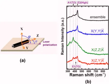
different polarization configurations of X¯ 共Y ,Y兲X, X¯共Z,Z兲X, and X¯ 共Y ,Z兲X according to the Porto notation were investi-gated, where the c axis of the nanorod is set as the Z axis. The term of X¯ 共Y ,Z兲X represents that the laser light is inci-dent from the opposite X direction with the Y polarization, while the scattered signal is collected with the Z polarization in the X direction. The coordination of the single ZnO nano-rod with respect to the incident/scattered light is shown in Fig.2共a兲. Figure 2共b兲 shows the Raman shift spectra of an individual ZnO nanorod with different polarization configu-rations. For comparison, the Raman signal of the as-grown ZnO nanorod array 共denoted as ensemble兲 was also mea-a兲Author to whom correspondence should be addressed. Electronic mail:
chunwei@ntu.edu.tw.
APPLIED PHYSICS LETTERS 92, 223102共2008兲
0003-6951/2008/92共22兲/223102/3/$23.00 92, 223102-1 © 2008 American Institute of Physics
sured. For the as-grown sample, the peaks at 331, 378, 410, and 438 cm−1can be resolved, which can be assigned to A1
共acoustic overtone兲, A1 共TO兲, E1 共TO兲, and E2 共high兲
sym-metry modes, respectively, which are consistent with those that reported the Raman shift signals of the bulk ZnO thin films or ensemble of nanostructures.17–19For the Raman shift signals of the individual ZnO nanorod, strong polarization dependence on Raman signatures can be found. In the X
¯ 共Y ,Y兲X configuration, where the incident/scattered photons
are polarized perpendicular to the c axis of the nanorod 共de-noted as E⬜兲, the peak at 438 cm−1 of the E
2 共high兲 mode
becomes dominant, accompanying a very weak intensity of A1 共TO兲 mode at 378 cm−1 and a negligible signal of the
peak at 331 cm−1. The relative intensity of the individual peaks in the E⬜configuration is similar to the Raman shift signatures of the ZnO nanorod array, which were grown along the c axis. In contrast, for the X¯ 共Z,Z兲X configuration, where the incident/scattered light has the polarization paral-lel to the c axis of the nanorod共denoted as E储兲, the peak at 378 cm−1 corresponding to the A
1 共TO兲 mode becomes
dominant with a large suppression of the E2 共high兲 mode at
438 cm−1. In addition, the peak of A1 共acoustic overtone兲
at 331 cm−1 also persists well in the E储 polarization condition. The Raman intensity I can be usually expressed as I⬃兩eˆs· RJ ·eˆl.兩2, where RJ is the Raman tensor and el= cosXˆ
+ sinsinYˆ + sincosZˆ, es= cosXˆ +sinsinYˆ + sin
cosZˆ, eˆl.共eˆs兲 is the unit vector of the incident 共scattered兲
light polarization and 共or兲 is the angle between the inci-dent共or scattered兲 light polarization and the nanorod axis. In our case, =/2 corresponds to the angle between the propagating direction of scattered light and the orientation of the nanorod axis. According to the theoretical prediction,11,12 when=, the intensity of the A1共TO兲 at 378 cm−1 should
become dominant when = 0° and the E2 共high兲 mode at 438 cm−1 should be dominant when = 90°, which shows a
good consistency with the above observation in the X¯ 共Z,Z兲X and X¯ 共Y ,Y兲X configurations, respectively. However, the non-zero signal at 438 cm−1 共or 378 cm−1兲 in the X¯共Y ,Y兲X 共or X
¯ 共Z,Z兲X兲 configuration is mainly attributed to nonperfect orientation of the nanorod with respect to the polarization of
FIG. 1.共a兲 The SEM micrograph of the well-aligned ZnO nanorods. The scale bar is 6m.共b兲 The SEM image of an individual ZnO nanorod. The scale bar is 100 nm.共c兲 High-resolution TEM image of an individual ZnO nanorod 共growth along the c axis兲 and the corresponding electron diffraction pattern.
FIG. 2.共Color online兲 共a兲 The coordination of the single ZnO nanorod with respect to the incident/scattered light.共兲 is the angle between the laser polarization and the Z axis共X axis兲. 共b兲 The Raman shift spectra of the single ZnO nanorod with different polarization configurations of X¯ 共Y ,Y兲X,
X
¯ 共Z,Z兲X, and X¯共Y ,Z兲X according to the Porto notation. The spectra of the
ensemble represents the Raman scattering spectra of the as-grown ZnO na-norod array.
223102-2 Chien et al. Appl. Phys. Lett. 92, 223102共2008兲
the incident/scattered light. As the polarization configuration is changed to X¯ 共Z,Y兲X, all the A1 共TO兲, E1 共TO兲, and E2 共high兲 modes appear. The above result clearly accounts for the nature of polarization-dependent anisotropy in the Raman spectra of an individual ZnO nanorod.
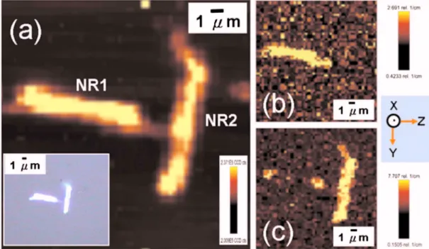
We have further chosen two individual ZnO nanorods with orientations almost perpendicular to each other to per-form the Raman scattering image mapping experiment. The inset in Fig.3共a兲shows the optical microscopic image of the two nanorods. By intensity integration of the spectral domain ranging from 250 to 900 cm−1, the Raman image of the two
individual ZnO nanorods, labeled as NR 1共nanorod 1兲 and NR 2共nanorod 2兲, can be obtained, as shown in Fig.3共a兲. By integrating the intensity of the spectral domain 共370–385 cm−1兲 around the A
1共TO兲 mode at 378 cm−1and
of the spectral domain共430–445 cm−1兲 around the E 2共high兲
mode at around 438 cm−1in the X¯ 共Z,Z兲X configuration, the
complementary images with the maximum signals almost on the portion of the NR1 and NR2 are obtained, as shown in Figs.3共b兲and3共c兲, respectively. The polarization of incident light is now pointing along the scale bar, as shown in Fig. 3共a兲, which is assigned as the Z axis. The result provides the information correlating the local phonon behavior with geo-metric and orientation-dependent anisotropy. However, the nonvanishing Raman intensity image at the two ends of the NR1 in Fig.3共c兲is possibly due to 共i兲 the nonperfect orien-tation of the NR1 or nonuniform crystal growth along the c axis with respect to the incident photon polarization or 共ii兲 the boundary mismatch of the dielectric function between a nanorod and its surroundings共air兲, which may also cause the strong dependence of the transmission of the light inside a nanorod on its shape, orientation and size.14,15,20
In summary, an individual ZnO nanorod has demon-strated a large anisotropy in its Raman scattering spectra when different incident/scattered light polarization configu-rations are used. The Raman image mapping signals provide
direct information accounting for the anisotropic phonon be-havior of the individual ZnO nanorods.
This work is supported by the National Science Council, Taiwan 共Project Nos. 96-2112-M-002-030-MY3 and NSC 96-2120-M-001-001兲. The authors would also like to thank Dr. Li-Chyong Chen for providing the SEM images.
1H. J. Ko, Y. F. Chen, Z. Zhu, T. Yao, I. Kaobayyashi, and H. Uchiki,Appl. Phys. Lett. 76, 1905共2000兲.
2W. I. Park, Y. H. Jun, S. W. Jung, and G.-C. Yi,Appl. Phys. Lett. 82, 964
共2003兲.
3D. M. Bagnall, Y. F. Chen, Z. Zhu, T. Yao, S. Koyama, M. Y. Shen, and T.
Goto,Appl. Phys. Lett. 70, 2230共1997兲.
4P. Zu, Z. K. Tang, G. K. L. Wong, M. Kawasaki, A. Ohtomo, H. Koinuma,
and Y. Segawa,Solid State Commun. 103, 459共1997兲.
5H. Co, J. Y. Xu, E. W. Seelig, and R. P. H. Chang,Appl. Phys. Lett. 76,
2997共2000兲.
6D. Snoke,Science 273, 1351共1996兲.
7J. D. Joannopoulos, P. R. Villeneuve, and S. Fan,Nature共London兲 386,
143共1997兲.
8C. W. Chen, K. H. Chen, C. H. Shen, A. Ganguly, L. C. Chen, J. J. Wu, H.
I. Wen, and W. F. Pong,Appl. Phys. Lett. 88, 241905共2006兲.
9J. C. Johnson, H. Yan, P. Yang, and R. J. Saykally,J. Phys. Chem. B 107,
8816共2003兲.
10P. J. Pauzauskie, D. Talaga, K. Seo, P. Yang, and F. Lagugne-Labarthet,J. Am. Chem. Soc. 127, 17146共2005兲.
11T. Livneh, J. Zhang, G. Cheng, and M. Moskovits, Phys. Rev. B 74,
035320共2006兲.
12C. L. Hsiao, L. W. Tu, T. W. Chi, M. Chen, T. F. Young, C. T. Chia, Y. M.
Chang,Appl. Phys. Lett. 90, 043102共2007兲.
13A. Hartschuh, E. Sanchez, X. S. Xie, and L. Novotny,Phys. Rev. Lett. 90,
095503共2003兲.
14J. Frechette and C. Carraro,J. Am. Chem. Soc. 128, 14774共2006兲. 15H. M. Fan, X. F. Fan, Z. H. Ni, Z. X. Shen, Y. P. Feng, and B. S. Zou,J.
Phys. Chem. C 112, 1865共2008兲.
16H. Harima,J. Phys.: Condens. Matter 14, R967共2002兲.
17T. C. Damen, S. P. S. Porto, and B. Tell,Phys. Rev. 142, 570共1966兲. 18M. Rajalakshmi, A. K. Arora, B. S. Bendre, and S. Mahamuni,J. Appl.
Phys. 87, 2445共2000兲.
19R. P. Wang, G. Xu, and P. Jin,Phys. Rev. B 69, 113303共2004兲. 20L. Cao, B. Nabet, and J. E. Spanier,Phys. Rev. Lett. 96, 157402共2006兲.
FIG. 3.共Color online兲 共a兲 Raman scattering mapping image of two individual ZnO nanorods with orientation almost perpendicular to each other. The inset in 共a兲 shows the optical image of ZnO nanorods. 共b兲 Raman images generated by integration of 共370–385 cm−1兲 and 共c兲 共430–445 cm−1兲 spectral ranges for the X共Z,Z兲X¯ polarization configuration.
223102-3 Chien et al. Appl. Phys. Lett. 92, 223102共2008兲