RTU3A-4
A
Miniature Low-Insertion-Loss, High-Power
CMOS SPDT Switch Using Floating-Body Technique
for
2.4-
and
5.8-GHz
Applications
Mei-Chao Yeh, Ren-Chieh Liu, Zuo-Min Tsai and Huei Wang
Dept. of
Electrical
Engineering and
Graduate
Institute of
Communication Engineering,
National
Taiwan
University, Taipei, 106, Taiwan, R.O.C.
Abstract - A low insertion loss SPDT switch in standard 0.18-
pm CMOS process was developed for 2.4- and 5.8-GHz WLAN
applications. In order to reduce the insertion loss and increase the PIdR, the floating-body circuit topology is proposed. The
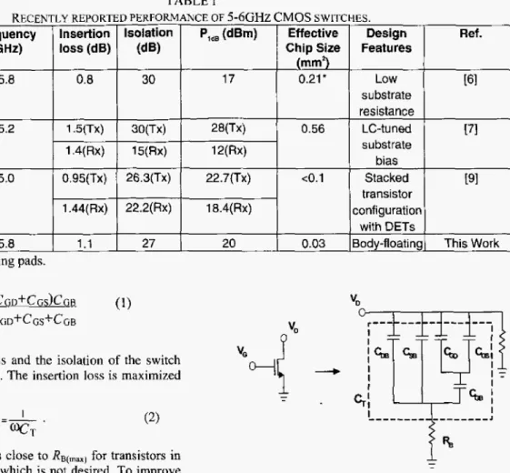
series-shunt switch achieves a measured PI,, of 20 dBm, an insertion loss of 1.1 dB, and an isolation of 27 dB at 5.8 GHz. It also achieves a measured insertion loss of 0.65 dB and'an isolation of 35 dB at 2.4 GHz. The effective chip size is only 0.03 mm'. The measured data agree with the simulation results well. To our knowledge, this work presents the low insertion loss, high isolation and good power performance with the smallest chip size among the previously reported 2.4- and 5.8-GHz CMOS switches.
Index Terms - CMOS, SPDT switch, body floating.
I. INTRODUCTION
In recent years, wireless communication systems have undergone explosive growth that is largely unanticipated.
Much of this growth has been in complementary metat-oxide semiconductor (CMOS) technology. CMOS technology has been able to meet the more stringent cost constraints inherent in these more diverse mainstream applications. The advantages of silicon CMOS technology for RF and microwave control functions over GaAs are its low cost structure and its integration potential with R F and silicon MOS-based mixed-signal circuitry. A high-quality microwave switch is a key building block of a RF front end for time- division duplexing (TDD) communication systems. To further increase the integration level, the SPDT switch has to be integrated in the transceiver.
Switches using high performance processes such as
GaA5
HEMTs were designed for digital mobile communication systems [ I ] , However, due to the advantages of low cost and integration capability with baseband circuits, the CMOS RF chips are getting more attractive. Key figures of merit of a TAX switch are insertion loss and power handling capability measured by the power ILdB compression point (F',d& [ 2 ] - [ 5 ] .Switches using high and low substrate resistances in a 0.18- pm CMOS process have demonstrated good insertion loss /6], but it requires a large area of substrate contact to implement a low substrate resistance switch. To achieve such performance, a LC-tuned substrate bias was used [7]. However, the bias network improving the large-signal handling capability increased the chip size greatly. In the meanwhile, the LC-
tuned substrate bias network limits the switch in a narrow frequency range. For 2.4-GHz and 5.2-GHz applications, two different switches are designed and the LC-tuned substrate bias networks are needed to be devised respectively. Impedance matching technique was used to improve the P,,,
of the switch [8], but the matching network resulted in a large die size, also. Switch realized by depletion-layer-extended transistors (DETs) obtained high power-handling
[SI.
Nevertheless, the DET5 are formed with the addition of more mask steps than the standard CMOS process, and in order to avoid latching up, the PMOS and n-well must be placed sufficiently far away from the DETs, and thus results in a Iarge chip size.In this paper, CMOS RF SPDT switches in standard 0.18- p m CMOS process are presented. Using the body-floating technique, this approach demonstrates high power-handling with a miniature chip size. The SPDT switch exhibits 0.65-dB insertion loss, 35-dB isolation at 2.4 GHz and 1.1-dl3 insertion loss, 27-dB isolation, 20-dBm output P,,, at 5.8 GHz. Table presents the recently reported performances of 5-6 GHz CMOS switches, Compared with the CMOS switches at 5.8 GHz, the chip accomplished the low insertion loss, high isolation, good power performance and smallest chip size simultaneously.
rI. BODY FLOATING TECHNIQUE
The SPDT switch is fabricated in a 0.18-ym CMOS process, which provides single poly layer for the gates of the MOS and six metal layers for inter-connection. As shown in Fig. 1, deep n-well (DNW) is offered as default in 0.18-pm mixed-signal process for better substrate isolation with an additional PN junction
[IO].
In this work, DNW is used to absolutely separate the body of the transistor with the p-substrate in the body-floating technique, Because of DNW, the switch can get rid of ta'tching up.The insertion loss of the switch was analyzed using the nMOS small signal model. As shown in Fig. 2, R, represents the substrate resistance associated with the transistor. C, stands for the equivalent capacitance and can be represented as:
0-7803-8983-2/05/$20.00 0 2005 IEEE
45 1
Process Frequency insertion Isolation ( G W loss (dB) (dB) 0.1 8-Fm CMOS 5.8 0.8 30 0.18-pm CMOS 5.2 1.5(Tx) 30(Tx) 1.4(Rx) 15(Rx) 0.1 8-ym
CMOS
5.0 0.95(Tx) 26.3(Tx) 1.44(Rx) 22.2(Rx) 0.18-pm CMOS 5.8 1.1 27From [ 2 ] , the insertion loss and the isolation of the switch are determined by C, and R,. The insertion loss is maximized when
P,,, (dBm) Effective Design Ref.
Chip Size Features
(mm') 17 0.21 * Low [GI substrate resistance substrate bias transistor with DETs 28(Tx) 0.56 LC-tuned [71 12(Rx) 22.7(Tx) <0.1 Stacked [91 18.4(Rx) configuration
20 0.03 Body-floating This Work
Usually, the value of
R B
is close to RB(,,,=) for transistors in the typical silicon processes which is not desired. To improve the insertion loss, the R, should be either extremely large or close to zero. In fact, it is impossible to makeR B
zero due to the parasitic effect, and thus how to let RB be large enough i s important. Furthermore, the parasitic capacitance associated with the body will seriously affect the impedance of the switch when the body of the transistor is connected to ground (RF short). Therefore, the body is connected to ground with 5 - kQ resistor as shown in Fig. 1. The resistor provides an open circuit for the RF signal to improve the insertion loss without affecting the impedance of the switch.Body floallng
1
I
r - - -
Drain Gale Souroe I Body
P
P
1
1
I
Deep-N-Well p - t y p ~ substrateFig. 1. A simple structure of DNW.
452
Fig. 2. model.
Small signal model for a NMOS operating in the passive
Drain
1
Gate 0-'
source Body-w
Fig. 3. Large-signal model of the device.
The body-floating technique also increases the power handling capability of the switch. Figure 3 shows the large- signal model of the device. In the on state, when the input power is high enough, the parasitic diodes between
drainkource and body will tum on. The waveform of the input signal is then clamped, and the
P,,,
of the circuit will be limited. When the body of the device is floating, the parasitic diodes will not turn on even if the input power is high enough, and thus the P,,, is improved. The simulated voltage waveforms of the output port of a 1 SO-pm series transistor are shown in Fig. 4, with the input power of 22 dBm. The difference between the peak values of the two different voltage waveforms is about 1.1V.pm.
The gate bias resistors R,,, R,,, R,, and R , are.5 k toimprove the dc bias isolation.
Tx Rx --C Body floating Body connected to gnd 6 I I I
-
2P
I 3 I I I I I I 0 50 100 150 200 250 300 350 Time (psec)Fig. 4. Simulated voltage waveforms of the output port in on-state transistor.
111. CIRCUIT DES~GN
By
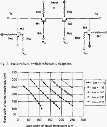
using body-floating technique, the insertion loss, isolation and power handling of the CMOS switch can be improved. Figure 5 is the schematic of the series-shunt CMOS RF SPDT switch which comprises two series and two shunt transistors. The series transistors MI and M2 perform the main switching function, and the shunt transistors, M3 andM4,
increase the isolation of the switch. It is observed that the ratio of the size for the series transistor to the shunt one significantly influence the performance of the switch, especially for the insertion loss. Figure 6 presents the simulated relation between the insertion loss and the gate width of series and shunt transistors. As can be observed, the size ratio of the series and shunt transistors must be selected properly. In order to achieve a low insertion loss, there are two choices: one is to use a large size for the series transistor and a small size for the shunt one, and the other i s simply the opposite, that is, to choose a small size for the series device and a large size for the shunt one. The series transistor with larger size has smaller parasitic resistance and thus attains lower insertion loss and better power performance. For the concern of power handling capability, large devices of 180- prn gate width are chosen for series transistors M1 and M2 in this design while the size of shunt transistors M3 and M4 is 60Fig. 5 . Series-shunt switch schematic diagram.
350
*
300 250 200 150 1 DO loss = 1.38 -A- 1 x 5 = 1.65 -1015 = 1.93 toss = 2 21 v '5 501
0 0 50 100 150 200 250 300Gate width of shunt transistors (pm)
Fig. 6 . The relationship between insertion loss and the sizes of the transistors. When the size ratio of the series and shunt transistors is
chosen propedy, the circuit has the lowest insertion loss.
Iv.
MEASUREMENT RESULTSThe die micrograph of the series-shunt SPDT switch using 0.18-pm CMOS process is shown in Fig. 7. The chip size is 0.53 x 0.37 mmz and the effective circuit area without pads is only 0.2 x 0.15 mm'. Tbe circuit was tested via on-wafer probing. As shown in Fig. 8, the series-shunt switch achieves an insertion loss of 0.65 dB and an isolation of 35 dB at 2.4 GHz. It also achieves an insertion loss of 1 . 1 dB and an isolation of 27 dB at 5.8 GHz. The measurements agree with the simulation results well. When the dc bias of the Tx and Rx nodes is 0 V,
V,,
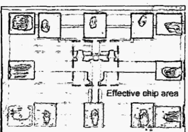
and V,, is 1.8 and 0 V respectively, the switch using 0.18-pm device achieves a P,,, of 20 dBm at 5.8 GHz as shown in Fig. 9. Using devices of the same sizes, another SPDT switch without body-floating technique achieves a PI,, of 18 dBm at 5.8 GHz. The P,,, of the switch is improved 2 dB by using the body-floating technique.Fig. 7. Die photograph of 0.18-pm CMOS switch. The effective circuit area without pads is only 0.03 mm’.
0 -10 -20 -30 -40 G-
o
%
0 3 Q m-
-
+ measurement d -50 -1 0 0 2. 4 6a
10 Frequency (GHz)Fig. 8. Insertion loss and isolation of the 0.1 8-pm CMOS switch. It achieves a 1.1-dB insertion loss and 27-dB isokation at 5.8 GHz.
Fig. 9. Insertion loss V.S. P,” of the 0.18-~m CMOS switch. Using the body-floating technique, the P,,,of the switch is improved 2 dB.
V. CONCLUSION
presented and
on
measurements in 0.18-pm devices. A SPDT switch has been designed, fabricated, and tested. Using body floating technique, it accomplishes the low insertion loss, high isolation, good power performance and smallest chip size simultaneously. The switch exhibits 1 .I-dB insertion loss, 27- dB isolation, and 20-dBm outputP,,,
at 5.8 GHz. Since the switch was fabricated using’ standard 0.18-pm CMOS technology, it can be easily integrated with other front-end circuits to implement CMOS transceivers without requiring any additional mask or post-processing steps.ACKNOWLEDGEMENT
The work is supported in part by Sunplus and National Science Council of Taiwan R.O.C. (NSC 93-2752-E-002-002- PAE, NSC 93-2219-E-002-016, NSC 93-2219-E-002-024 and NSC 93-22 13-E-002-033).
REFERENCES
[ l ] K. Miyatsuji, S. Nagata, N. Yoshikawa, K. Miyanaga, Y . Ohishi, D. Ueda, “A GaAs high-power RF single-pole double-throw switch IC for digital mobile communication system,” IEEE ISSCC1994 Dig. Tech. Papers, pp. 34-35.
“A 0.5” ‘CMOS T/R
switch for 900-MHz wireless applications,” IEEE J. Solid- Stute Circuirs, vol. 36, pp. 486-492, May 2000.
[3] Aruna Ajjikuttira, Chester Lmng, Ee-Sze Khoo. Mark Choke, Rajinder Singh, “A fully-integrated CMOS RFTC bluetooth application,” IEEE ISSCC2001 Dig. Tech. Papers, pp. 198-199. [4] Kenneth K.0, Xi Li, Feng-Jung Huang, and William Foley,
“CMOS components for 802.1 1 b wireless LAN applications,” IEEE RFlC Symp., pp.103-106,2002,
[SI M. Madihian, L. Desclos, T. Drenski, “CMOS RF ICs for 900MHz-2.4GHz band wireless communication networks,”
[6] Zhenbiao Li, Hyun Yoon, Feng-Jung Huang, and Kenneth K. 0,
“5.8-GHz CMOS TIR switches with high and low substrate resistances in a 0.18-pm CMOS process,” IEEE Micrnwuve Wireless Comp. Lett.. vol. 13, Jan 2003.
[7] Niranjan Talwalkar, C Patrick Yue, and S . Simon Wong, “An
integrated 5.2GHz CMOS T/R switch with LC-tuned substrate
bias,” IEEE ISSCC2003 Dig. Tech. Papers, pp. 362-363, 2003.
[8] Feng-Jung Huang, and Kenneth K. 0, “Single-pole double-throw
CMOS switches for 900-MHz and 2.4-GHz applications on p-
silicon substrates,” IEEE J. Solid-State Circuits, vol. 39, January 2004.
[9] Takahiro Ohnakado, Satoshi Yamakawa, Takaaki Murakami, Akihiko Furukawa, Eiji Taniguchi Hiro-omi Ueda, Noriharu Suematsu, and Tatsuo Oomori, “2 1.5-dBm power-handling 5-
GHz transmivreceive CMOS switch realized by voltage division effect of stacked transistor configuration with depletion-layer- extended transistors (DETs),” IEEE J. Solid-state Circuits, vol.
39, January 2004.
design guideline.
[2] Feng-Jung Huang and Kenneth 0,
IEEE RFlCSymp., pp. 13-16, 1999.
[ 101 TSMC 0 . 1 8 ~ m mixed signal 1P6M+ MIM salicide 1 .8V/3.3V
CMOS technology is a promising technology for RF and microwave control elements based upon the circuit model