283
Mobility and oxide breakdown behavior in ultra-thin oxide with atomically smooth interface
Y. C. Cheng, W. J . Chen,' B. C. Lin, C. Tsai, and Albert Ch' In Dept. Of Electronics Eng., National Chiao Tung Univ., Hsinchu, Taiwan
'Dept. Of Mechanical Materials Eng., National Yun-Lin Polytechnic Inst., Huwei, Taiwan China Tel: +886-3573-1841; Fax: +886-3572-4361; E-mail: achin@cc.nctu.edu.tw
Abstract
The device performance made by thin gate oxide is related t o the oxide thickness uniformity and the interface smoothness Unfortunately, native oxide roughens the initial surface before thermal oxidation. In this paper, we have designed a leak-tight low-pressure N2O oxidation system, and the native oxide is desorbed in-sifrt under HZ environment. Atomically smooth oxide and Si interface of ultra-thin oxides (1 1-38A) were achieved as observed by high-resolutional TEM. Significant mobility enhancement over large gate field is obtained by reducing interface roughness scattering. The oxide reliability is also improved by this smoother interface between Si and oxide.
I. INTRODUCTION
Scaling down the thickness of gate oxide [1]-[6] is one of the most important factors to continuously improve both CMOS devices and circuit performance. Ultra-thin 1 SA-oxide [4] has demonstrated excellent device performance and direct-tunneling oxide with thickness less than 308, is required for deca-nano CMOS technology. However, the presence of native oxide becomes an increasing concern for these thin oxides; it is reported that the naive oxide will strongly degrade the oxide reliability. To avoid the native oxide formation, several oxidation processes have been proposed recently. including a closed wet cleaning environment and H-terminated Si. Another native oxide related problem for these thin oxides is the interface roughness. The interface roughness can strongly affect the carrier transport that can be
characterized by measuring the electron mobility of MOSFET's [7]-[9]. Furthermore, electron mobility is an important parameter related t o current drive and operation speed of MOSFET's. In this paper, we have developed a new oxidation process. Very smooth interface of oxidel5 is achieved by irr-silo desorbing the native oxide in a low-pressure oxidation system before initiating thermal oxidation. Atomically smooth interface between oxide and Si is observed by high- resolution TEM for oxide thickness of 1 1 and 38A, The atomically smooth oxide is hrther characterized by measuring the electron mobility. Significant mobility increase is observed in these oxides with atomically smooth interface. Because the smooth interface and uniform thickness of oxide, the reliability is also much improved.
11. EXPERIMENTAL
We have designed a low-pressure oxidation system to desorb native oxide in-sitit before initiating the growth of thermal oxide. A leak- tight reactor design and a high flow rate of hydrogen are used to avoid pre-matured growth of native oxide during temperature ramping up. Similar process procedure has been used in LPCVD to grow high quality Si epitaxy at 550°C [IO]. After desorbing the native oxide by hydrogen bake, thermal oxides were grown at 900 "C using N2O. To achieve better thickness controllability, the oxides were grown under a reduced pressure of 4.5 torr. Another merit of oxides grown under reduced pressure is the increased mean-free-path of oxygen molecules.
284
Therefore excellent thickness uniformity of variation less than 0.5A is obtained across 4-inch wafer for a typical 20A oxide. By using the above process, ultra-thin 1 I
A
oxide can be continuously obtained. To reduce the initial Si surface roughness, a modified RCA cleaning is used with lower NHJOH and,HF,
contents to achieve a smoother surface before oxidation. As measured by AFM, the RMS roughness is in a range between 1.5 to 2A. For comparison purpose, control samples were grown under similar condition except without i?i-.s/tii cleaning thenative oxide. These oxides were hrther characterized by high-resolution. TEM, interface mobility, and stress measurement.
111. RESULTS AND DISCUSSION
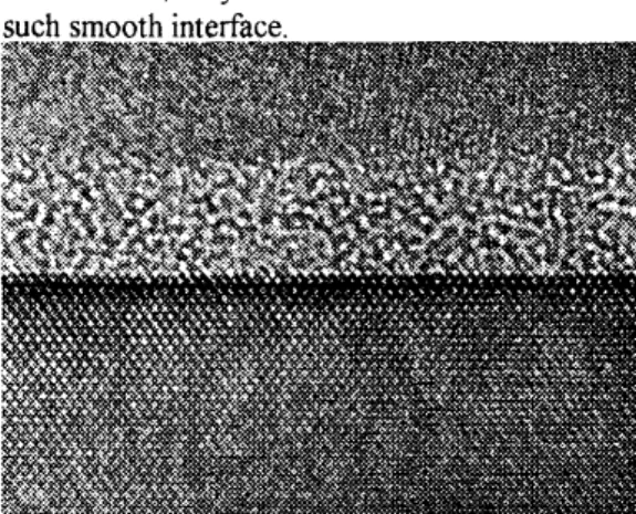
As mentioned above, one of the most important factors for oxide is the thickness uniformity and the related interface smoothness. Because of the uniform thickness, electric field can be evenly distributed over the whole oxide. On the other hand, a rough interface will generate local high electric field and therefore large current will flow through these areas and create reliability problem. Furthermore, the smooth interface is essential to achieve better electron mobility and switching speed of devices. Therefore we have first measured the interface roughness between oxide and Si. We have used cross-sectional TEM to observe this interface roughness. Fig. 1 presents the cross-sectional picture of the 38A oxide with in-sitti native oxide cleaned by hydrogen bake. The oxide thickness can be measured from the atomic image of single crystalline Si underneath the oxide; the distance between two adjacent planes in (1 11) direction is 3.1A. It is important to note that atomically smooth interface between oxide and Si can be achieved and this is the best reported interface smoothness of oxide. Because such smooth interface is almost impossible to achieve after wet cleaning even using the modified RCA cleaning process,' surface Si atom migration, after desorbing native oxide under a hydrogen
environment, may be the mechanism to achieve
Fig. f . High-resolutional TEM image of the 38.4 oxide with in-situ native oxide cleaned.
Because our process can in-sitii desorb the native oxide, ultra-thin thermal oxide can be grown on fresh Si surface with thickness comparable to native oxide. Fig. 2 shows the cross-sectional TEM image of this ultra-thin 1 l A oxide. One important feature is that the 1 IA oxide is oxidized only by two atomic Si layers. Therefore this 1
IA
oxide may set up the ultimate and practical limit for further oxide thickness scaling.Fig. 2. High-resolutional TEM image of the 1lA oxide
285
Because the interface roughness is one of the dominant factors to limit the electron mobility over wide electric field range, we have firther investigated the electron mobility improvement of these oxides with atomicallv smooth interface.
1000
~. . .
. . . . ..
I o4 10' IO" IO'
Effective Field( V h n )
Fig. 3. Dependence of electron mobility on norinal electric field of the 70A oxides. Both samples are fabricated in the same lot and the only difference is the additional hydrogen bake step to desorb native oxide.
Fig. 3 shows the comparison of measured mobilities of control oxide grown by conventional method and the oxide with atomically smooth interface, respectively. The mobility is calculated from the measured channel conductance of wide gate MOSFET's. The thickness of both oxides is about 70A. The electron mobility of control oxide follows the typical mobility and field dependence [7]-[9]. In contrast, near 30% increased mobility is measured over wide effective normal field from the MOSFET with atomically smooth interface. This is the best reported mobility value at the same effective normal field. Because both wafers from control oxide and atomically smooth oxide were processed at the same lot, the measured electron mobility enhancement is not process- related. Therefore the mobility enhancement is strongly related to the improved interface smoothness as observed by cross-sectional TEM. Further, the measured mobility improvement is consistent to the theoretical prediction; the
interface roughness dominates the high-field electron mobility that is also observed in measured data It is important to note that the 30% mobility improvement related device performance enhancement is equivalent t o the improvement by one generation of VLSI technology with 70% reduction of gate length
. . 001
4.4' " " " ' I . ' 0
aa,
a
EOD a a , . l a X ,sbesstim(sec)
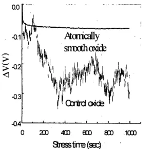
Fig. 4. Dependence of voltage'change on stress time of tlic
27A oxides under a constanl current density of 10Ncin'. The voltage noise in control oxide is-the Vpical soft brcakdown phenomenon.
Another important factor testing the oxide integrity will be the reliability. Fig. 4 shows the oxide stress data under a large applied constant current density of 10A/cm2. Because of the small change in voltage, we have plotted the voltage change instead of voltage value. A large current density is used here because no measurable change can be observed under lower current density stress for oxide with atomically smooth interface. For both oxides, there is no hard breakdown can be observed even under a large injected charge of 10' C/cm2. Instead of hard breakdown, control oxide shows a soft breakdown behavior that is generally observed in thin oxides. In sharp contrast, oxide with atomically smooth interface did not show any soft
286
breakdown behavior. Although possible mechanism of soft breakdown is still not understood, a smoother oxide surface may distribute the applied electric field more uniformly and therefore ’ reduce the possibility of soft
breakdown
IV. CONCLUSIONS
In conclusion, we have developed a new oxidation process to achieve atomically smooth interface between oxide and Si. Electron mobility improvement as much as 30% is obtained by using these smooth oxides, while the related MOSFET performance improvement is equivalent to one VLSI generation. In addition to the measured higher electron mobility, much improved oxide reliability
is
also achieved and no soft breakdown can be measured even under a large charge injection of IO“ c/crn2.ACKNOWLEDGMENTS
We would like to thank the helpful discussion from Prof K. C. Hsieh at the Dept. of Electrical engineering, Univ. of Illinois, and thank the continuous support from Prof T. F. Lei at our Department. This work has been supported by NSC (87-221 5-E-009-069) of Taiwan.
Reference:
[ I ] H. Hwang, W. Ting, D. L. Kwong, and J. Lee,
“Improved reliability characteristics of submicrometer nMOSFETs with oxynitride gate dielectric prepared by rapid thermal oxidation. in N20,” IEEE .Eleclron Dcvice Lelt., vol. 12, no 9, pp. 495-497, 1991.
[2] M. Bhat, D. Wristers, J. Yan, L. K. Han, J. Fulford, D. L. Kwong, “Performance and hot-carrier reliability of N- and P-MOSFETs with rapid thermally NO-nitided S O 2 gate dielectrics,” in IEDM 7ech. D i g , 1994, pp. [ 3 ] C. T. Liu. Y. Ma, H. Luftman, and’ S. J. Hillenius, “Preventing boron penetration through 25-A gate oxides with nitrogen implant in the Si substrates,” IEEE Electron
329-332.
Device Lett., ‘vol. 18, no 5 , pp. 212-214,
1997.
[ 4 ] H. S . Momose, M. Ono, T. Yoshitomi, T. Ohguro, S. Nakamura, M. Saito, and H. Iwai, “1.5 nm direct-tunneling gate oxide Si MOSFET’s,” IEEE Tram Electron Devices,
[ 5 ] W. R. Anderson, D. R. Lombardi, R.
G.
Wheeler,
T.
P. Ma, “Determination of Si/SiOz interface roughness using weak localization,” IEEE Electron Device Lett., vol. 14, no 7 , pp.[6] K. F. Lee, R. H. Yan, D. Y. Jeon, G. M. Chin, Y. 0. Kim, D. M. Tennant, B. Razavi,H. D. Lin, Y. G. Wey, E. H. WestenvickM. D. Moms, R. W. Johnson, T. M. Liu, M. Tarsia, M. Cerullo, R. G. Swartz, and A. Ourmazd, “Room temperature 0.1 pm CMOS technology with 1 1.8 ps gate delay,” in
IEDM
Tech. Dig.,1993,.pp. 131-134.
[7: J. Hauser, “Extraction of experimental mobility data for MOS devices,” IEEE Trans. Electron Devices, vol. 43, no. 1 1 , pp. 1981-
1988, 1996.
[SI S. C. Sun and J. D. Plummer, “Electron mobility in inversion and accumulation layers on thermally oxidized silicon surfaces,” IEEE
Trans. Electron Devices, vol. 27, no. 8, pp.
[ 9 ] H. Shin, G. M. Yeric, A. F. Tasch, and C. M. Maziar, “Physically-based models for effective mobility and local-field mobility of electrons in MOS inversion layers,” Solid-
State Electron., vol. 34, no.6, pp. 545-552,
1991.
[ I O ] A. Chin, B. C. Lin, and W. J. Chen, “High quality epitaxial Si grown by a simple low- pressure chemical vapor deposition at 550 degrees C,” Appl. Phy.s. Lett., vol. 69, no. 1 1, vol. 43, no.8, pp. 1233-1241, 1996.
3 5 1 - 3 5 3 , 1993.
1497-1508, 1980.