IEEE PHOTONICS TECHNOLOGY LETTERS, VOL. 20, NO. 18, SEPTEMBER 15, 2008 1575
Single-Period InAs–GaAs Quantum-Dot Infrared
Photodetectors
Shu-Ting Chou, Member, IEEE, Shih-Yen Lin, Member, IEEE, Chi-Che Tseng, Student Member, IEEE,
Yi-Hao Chen, Cheng-Nan Chen, and Meng-Chyi Wu, Senior Member, IEEE
Abstract—In this letter, we investigate the performance of
single-period InAs–GaAs quantum-dot (QD) infrared photodetectors, in which the single-period QD is sandwiched by different thicknesses of the undoped GaAs confinement layers. By using a 5-nm p-type GaAs layer as a current blocking barrier, the investigated three devices exhibit no response, the highest response, and the medium response, respectively. It is attributed to three different electron occupancy situations in the QD region resulted from the various locations of the Fermi level. A higher barrier for the thermionic emission current is observed for the device with a lower Fermi level in the QD structure. It is attributed to the acceptor-like behavior of the depleted QD such that a higher barrier height would be ob-served.
Index Terms—Quantum dot (QD), quantum-dot infrared
pho-todetector (QDIP).
I. INTRODUCTION
M
ULTISTACKED quantum-dot infrared photodetectors (QDIPs) have attracted much attention in recent years [1]–[7]. Compared with the conventional quantum-well infrared photodetectors, device performances such as high-temperature operation and absorption over normal incident light have been reported [1]–[5]. Among all the previous reports, most QDIPs are of multistacked quantum-dot (QD) structure embedded between two n-type GaAs contact layers. The thick undoped GaAs region in the device structure of QDIPs is helpful to reduce the theromionic emission current for the devices op-erated at higher temperatures and higher voltages. To further suppress the dark current, the barrier layer with a higher con-duction-band discontinuity such as the AlGaAs layer is also included in the device structures [6], [7]. Large-format QDIP focal-plane arrays based on the structures for thermal imaging applications have been also developed [8], [9]. Although great success has been achieved by using the multistacked QDIP structures, high-uniformity epitaxial growth is always very challenging due to the strain accumulation resulted from theManuscript received April 22, 2008; revised June 13, 2008. This work was supported in part by the National Science Council, Taiwan, under Grant NSC 96-2221-E-001-030.
S.-T. Chou is with the Research Center for Applied Sciences, Academia Sinica, Taipei 11529, Taiwan, R.O.C.
S.-Y. Lin is with the Research Center for Applied Sciences, Academia Sinica, Taipei 11529, Taiwan, R.O.C., and also with the Department of Pho-tonics, National Chiao-Tung University, Hsinchu 300, Taiwan, R.O.C. (e-mail: [email protected]).
C.-C. Tseng, Y.-H. Chen, C.-N. Chen, and M.-C. Wu are with the Department of Electrical Engineering, National Tsing Hua University, Hsinchu 300, Taiwan, R.O.C.
Digital Object Identifier 10.1109/LPT.2008.928847
TABLE I
SAMPLESTRUCTURES OFDEVICESA, B,ANDC
multistacked QD structures. Therefore, the QDIP structure with a few periods or even single period would greatly improve the uniformity and strain accumulation of the epitaxial wafers, which is important for the fabrication of detector arrays. The other issue concerned for the fabrication of QDIPs with a few periods is the possible weak responsivity of the devices. In this case, the position of QD structure in the device is critical for the optimized design and performance of QDIPs. In this letter, we report the effects of GaAs confining layer thickness on the single-period InAs–GaAs QDIPs prepared by molecular beam epitaxy (MBE). The highest responsivity can be observed for the device with the Fermi level inserted between QD ground state and excited state. The enhanced barrier height observed for the devices with lowering the Fermi level location in the QD structure would lead to the acceptor-like behaviors of the depleted QDs.
II. EXPERIMENTS
Three device structures with the single-period QD were prepared by the solid-source Riber P32 MBE system on the (100)-oriented semi-insulating GaAs substrates. The three de-vice structures are shown in Table I. For all the dede-vices, the
300-and 600-nm n-doped cm GaAs layers were
used as the top and bottom contact layers, respectively. A 50-nm undoped GaAs layer was then grown on the n-doped GaAs
bottom contact layer. A thin 5-nm p-type cm
GaAs layer was grown between the undoped GaAs confinement region and the 50-nm undoped GaAs layer as a current blocking barrier. The undoped GaAs confinement region consisted of two GaAs layers with a thickness of and on the top and bottom sides, respectively, which sandwiched a single 2.4-ML InAs QD layer. Keeping the same total undoped GaAs layer thickness of 300 nm, devices with different parameters
in the confinement region of (210, 90), (240, 60), and (270, 30)
1576 IEEE PHOTONICS TECHNOLOGY LETTERS, VOL. 20, NO. 18, SEPTEMBER 15, 2008
Fig. 1. Highest 10 K spectral responses of Devices B and C at 00.4 and 00.25 V, respectively.
in the unit of nanometers are referred to as Samples A, B, and C, respectively.
After mesa formation and metal evaporation, 100 100 m devices were fabricated. The bottom contact was always grounded while a positive or negative bias was applied onto the top contact. The spectral response was measured under an edge-coupling scheme [5]. For this purpose, the devices were 45 -off polished at one side of the samples. The infrared light was normally incident to the polished surface. The measure-ment system for spectral response consisted of a Spectral 100 Fourier transformation infrared (FTIR) spectroscopy coupled with a Janis cryostat and a current preamplifier. A tempera-ture-dependent dark current of the devices was measured by using a Keithley 236 source measure unit coupled with the same cryostat.
III. RESULTS ANDDISCUSSION
No spectral response can be observed for Device A. The highest 10 K spectral responses of Devices B and C at 0.4 and 0.25 V, respectively, are shown in Fig. 1. The reduced operation voltage of Device C is attributed to its higher dark currents, which would be shown in the later sections. Similar to the multistacked QDIPs [5], [7]; both devices also exhibit a wide detection wavelength range of 4–10 m. The results suggest that even with one single-period QD layer, the variation of QD size still broadens the detection window of the QDIPs. Also observed in Fig. 1 is the higher responsivity of Device B. Because the only difference among the three device structures is the single-period QD position in the undoped GaAs layers, one possible explanation is the different Fermi level locations with the electron occupancy situations in the QD structure for the three devices. Compared with conventional multistacked QDIPs, weaker responsivities are observed for the single-period QDIPs. However, by changing the single QD position, devices with observable response operated under low applied voltages could be achieved as in the cases of Devices B and C.
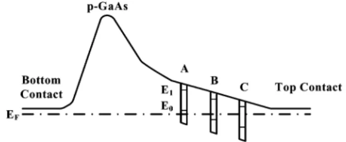
A schematic energy band diagram in the thermal equilibrium for the three devices is shown in Fig. 2. Because the p-type GaAs barrier layer has only a thickness of 5 nm, the Fermi level would be still close to the GaAs conduction-band edge to avoid the electron depletion in the QD structure for all three devices. Con-sidering the performances of the three devices, the most possible
Fig. 2. Schematic energy band diagrams in the thermal equilibrium of the three devices with the single-period QDs inserted at different locations of the undoped GaAs confinement region. Symbols A, B, and C represent the QD locations of Devices A, B, and C, respectively.
Fig. 3. The 10 K dark currents of Devices A, B, and C.
Fermi level positions for Devices A, B, and C should be 1) below the QD ground state, 2) between the QD ground and the excited states, and 3) close to the QD excited state, respectively. In case (1), most electrons are fully depleted from the QD structure and thus no response would be observed for Device A. For Device B, the highest responsivity observed among the three devices is resulted from its highest absorption coefficient. As for Device C, because the Fermi level is much higher than the QD ground state, reduced operation voltages would be obtained for this de-vice, as compared to Device B. In this case, a lower respon-sivity would be observed for the device. The results suggest that a proper location of the single-period QD structure is critical for the optimized performance of the devices.
To further investigate the transport characteristics of the QDIPs, the activation energy of the three devices is obtained via the curve fitting over the temperature-dependent dark current by assuming the dominant current to be the thermionic emission current [5]. The zero-bias activation energies obtained are 458, 425, and 402 meV for Devices A, B, and C, respec-tively. It is interesting to note that although the three devices are of similar structures, Device A has a lower Fermi level location in the QD structure, which would lead to a higher barrier and thus a lower dark current. Fig. 3 shows the 10 K dark currents of Devices A, B, and C. Inspection of Fig. 3 reveals that Device A exhibits the lowest dark current while Device C has the highest dark current. A possible mechanism responsible for this phenomenon is that the depleted InAs QDs would act like acceptors in the structure. In this case, the barrier height would be pushed to a higher level, as the case observed for Device A.
CHOU et al.: SINGLE-PERIOD InAs–GaAs QDIPs 1577
Fig. 4. The 10 K photocurrent and dark current of Device C.
Another phenomenon observed is that no response can be ob-served for the three devices under positive biases. To explain the results, the 10 K photocurrent and dark current of Device C are shown in Fig. 4. Inspection of this figure reveals that the photocurrent of Device C under positive biases are of the order lower than A at a positive bias below 1.5 V. Neverthe-less, the photoresponse is too low to be detected. The applied voltages to be positive or negative are defined according to the voltage polarity applied to the top contact. Another observation for Device C in Fig. 4 is the lower current under positive biases than that under negative biases. The reason lies at the enhanced barrier height of this device under positive biases such that the electron transport from the bottom contact to the top contact be-comes very difficult. In this case, either the dark current or pho-tocurrent of Device C would experience the same difficulty. The results would be the reduced photocurrent of the three devices under positive biases such that no response could be observed. The same mechanism also limits the photovoltaic (PV)-mode operation of the single-period QDIPs even for the device struc-ture with a built-in electric field, as discussed above. Electrons at the bottom contact could not tunnel through the barrier to com-pensate the loss of photoexcited electrons driven by the built-in electric field. Therefore, no PV-mode response can be observed for the devices.
IV. CONCLUSION
We have demonstrated the effects of GaAs confining layer thickness for the 2.4-ML InAs single QD layer on the
single-period InAs–GaAs QDIPs grown by MBE. By raising the Fermi level from near/below the ground state to close/above the excited state, Devices A, B, and C exhibit no response, the highest response, and medium response, respectively. These phenomena are attributed to three different electron occupancy situations in the QD region: 1) electrons fully depleted from the QDs, 2) electron fully occupied the ground states with most of excited states remained empty, and 3) electron partially occupied the excited states. Also observed is the lowering of barrier height with raising the Fermi level location in the QD structure. It is attributed to the acceptor-like behavior of the depleted InAs QDs such that the p-type GaAs barrier height would be pushed to a higher level.
REFERENCES
[1] S. F. Tang, S. Y. Lin, and S. C. Lee, “Near-room temperature operation of InAs/GaAs quantum dot infrared photodetector,” Appl. Phys. Lett., vol. 78, pp. 2428–2430, 2001.
[2] L. Jiang, S. S. Li, N. T. Yeh, J. I. Chyi, C. E. Ross, and K. S. Jones, “In Ga As=GaAs quantum-dot infrared photodetector with op-erating temperature up to 260 K,” Appl. Phys. Lett., vol. 82, pp. 1986–1988, 2003.
[3] S. Chakrabarti, A. D. Stiff-Roberts, P. Bhattacharya, S. Gunapala, S. Bandara, S. B. Rafol, and S. W. Kennerly, “High-temperature opera-tion of InAs–GaAs quantum-dot infrared photodetectors with large re-sponsivity and detectivity,” IEEE Photon. Technol. Lett., vol. 16, no. 5, pp. 1361–1363, May 2004.
[4] S. Y. Lin, Y. R. Tsai, and S. C. Lee, “The comparison of InAs/GaAs quantum dot infrared photodetector and GaAs/(AlGa)As superlattice infrared photodetector,” Jpn. J. Appl. Phys., vol. 40, pp. L 1290–L 1292, 2001.
[5] S. T. Chou, M. C. Wu, S. Y. Lin, and J. Y. Chi, “The influence of doping density on the normal incident absorption of quantum-dot in-frared photodetectors,” Appl. Phys. Lett., vol. 88, pp. 173511–173513, 2006.
[6] S. F. Tang, S. Y. Lin, and S. C. Lee, “InAs/GaAs quantum dot infrared photodetector (QDIP) with double Al Ga As blocking barriers,”
IEEE Trans. Electron Devices, vol. 49, no. 8, pp. 1341–1347, Aug.
2002.
[7] S. Y. Lin, Y. R. Tsai, and S. C. Lee, “High-performance InAs/GaAs quantum-dot infrared photodetector with single-sided Al Ga As blocking layer,” Appl. Phys. Lett., vol. 78, pp. 2784–2786, 2001. [8] S. D. Gunapala, S. V. Bandara, C. J. Hill, D. Z. Ting, J. K. Liu, S. B.
Rafol, E. R. Blazejewski, J. M. Mumolo, S. A. Keo, S. Krishna, Y. C. Chang, and C. A. Shott, “Long-wavelength infrared (LWIR) quantum dot infrared photodetector (QDIP) focal plane array,” Proc. SPIE, vol. 6206, p. 62060J, 2006.
[9] S. F. Tang, C. D. Chiang, P. K. Weng, Y. T. Gau, J. J. Ruo, S. T. Yang, C. C. Shih, S. Y. Lin, and S. C. Lee, “High-temperature op-eration normal incident 2562 256 InAs–GaAs quantum dot infrared photodetector focal plane array,” IEEE Photon. Technol. Lett., vol. 18, no. 8, pp. 986–988, Apr. 15, 2006.