M. N. Ou , S. R. Harutyunyan , S. J. Lai, C. D. Chen, T. J. Yang, and Y. Y. Chen 1 Institute of Physics, Academia Sinica, Taipei, Taiwan, ROC
2 Department of Electrophysics, National Chiao Tung University, Hsinchu, Taiwan, ROC 3 Institute for Physical Research, NAS, Ashtarak-2, Armenia
Received 11 May 2007, revised 3 October 2007, accepted 20 October 2007 Published online 12 December 2007
PACS 65.80.+n, 73.63.Bd
The thermal conductivity (κ), specific heat (Cp) and the resistivity (ρ) of a single nickel nanowire have been measured in the temperature range from 4 to 300 K by means of the “self heating 3ω” technique. Starting with a 100 nm nickel film grown on a Si/Si3N4 substrate by thermal evaporation, a suspended ni-ckel nanowire was then fabricated through e-beam lithography and etching processes. The width and length of the wire were determined by scanning electron microscope (SEM) as 180 nm and 35 µm re-spectively. At 300 K the thermal conductivity of nanowire is ~ 20% of the bulk, it diminishes to lower value as temperature decreases. The consequence is opposite to that of the bulk and might be explained by the ristriction of mean free paths of electron/phonon–phonon interactions due to the grain boundaries. An enhancement of specific heat ~250% of the bulk is also observed. In addition, the resistivity of nano-wire at room temperature is about four times larger than that of the bulk. The small relative resistiv-ity ra-tio (RRR) confirms the polycrystalline characteristic of the nanowire.
© 2007 WILEY-VCH Verlag GmbH & Co. KGaA, Weinheim
1 Introduction
Metallic nanowires were studied intensively during recent years due to their great importance in funda-mental low-dimensional physics as well as in technology [1]. This paper presents the study of electrical and thermal transport of suspended nickel (Ni) nanowires. Ni is one of the three elementary ferromag-netic transition metals, and understanding the properties of this pure metal is stimulated by considerable interest in fabrication of nanoscale magnetic devices. Although there are a number of publications on electrical resistivity and magnetoresistivity of Ni nanowires in literature [2, 3], the data on heat transport in this material are suffering from the lack of information.
By now, it is known that nanowires consist of the enhanced numbers of interfaces, which are always related to random atomic arrangements and superimposed by vacancy like defects. These interfaces have strong scattering ability to conduction electrons and therefore cause additional resistivity. At this condi-tion when the grain size of nanowire is comparable to the electron mean free path (MFP), each crystallite acts like a potential well with interface as a barrier. As a result, the effective number of the conduction electrons is limited to those which tunnel through all the boundaries along the MFP. In this case the be-havior of charge current at disordered condition can differ from the bebe-havior of heat current even though the heat current carriers are the same charged particles. In addition for disordered nanowires when charge current is strongly restricted the role of phonons in the temperature range θ /20 < T < θ would be
im-phys. stat. sol. (b) 244, No. 12 (2007) 4513 Paper
2 Experimetal details
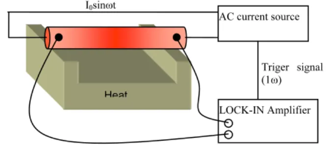
To prepare a single nickel nanowire (Ni-NW), we have developed the lithography process which com-binded the e-beam lithography, thermal evaporation technology to form a suspended single nanowire. The single nickel nanowire was fabricated with following process: (1) form wire pattern by e-beam li-thography technology, (2) deposition with thermal evaporator on Si/Si3N4 substrat at RT followed with solution lift-off process, (3) form the etching-window by e-beam lithography tech., (4) dry-etching (Re-active-ion etching with gas CF4, high pressure ~ 0.25 mTorr) and (5) anisotropic wet-etching (KOH, 27 w%, 85 °C). Figure 1 shows the suspended single Ni-NW combined with four-probe circuit, the stress induced by the sagging of wire is taken into account in our measurements.
Fig. 1 The SEM image of suspended nickel single nanowire with 4-probes measurement circuit. The dimensions of nanowire are 35 µm x 180 nm x 100 nm.
Usually, the various properties (κ(T), σ(T), C(T)) are measured by different instruments even using the different specimen. In the applied 3ω-method [4] the three depenencies are measured on the same speci-men and at the same mospeci-ment and envirospeci-ment. The measurespeci-ment setup was shown in Fig. 2. A junction-free design has been made to prevent the measurement error which could be caused by unexpected them-perature variation of contacts. The current-injection electrodes (contact area) are placed far away from Ni-NW to minimize the influence of contact heating.The thermal contact of the nanowire at the two ends to substrate was good enough to satisfy the measurement condition of 3ω-method. Note that the heating power of the suspended Ni-NW is about 1 ppm of nonsuspended one.The whole set of base and speci-men are placed in a OXFORD He3-refrigerator probe which provides high vacuum and ultra-low tem-perature down to 0.5 K.
Fig. 2 The measurement setup.
3 Results and discussion
Figure 3 shows the experimental data of the thermal conductivity κ in the temperature region of 15-300 K and the electrical resistivity ρ in the temperature region of 0.5-300 K for the Ni nanowire. Although, temperature dependence of the electrical resistivity for nanowire is metallic, it is found that the absolute magnitude of the electrical resistivity is greatly increased from corresponding bulk one, showing in-creased residual resistivity. The resistivity ratio of resistivity at room temperature 300 K to that at 4 K are 2 and 47 for nanowire and bulk sample correspondingly. Since the wire dimensions are much larger than the mean free path of Ni then this enhancement in resistance value is owing to the effect of grain– boundary scattering which is appeared to be predominant. It is needed to say that in nanocrystalline ma-terials the resistivity temperature behavior ρ(T) is controlled by both phonon scattering, and interfacial scattering, and interfacial scattering enhances with decreasing temperature [5, 6]. If the interfacial scat-tering becomes dominant, then the total resistance will possibly increases with decreasing temperature, showing nonmetallic behavior. In our case, obviously, we have some intermediate situation i.e. the in-creased but not dominant interfacial scattering and we can claim that the enhanced disorder for the given nanowire does not affect so crucial the current carrying process in it. The situation is changed drastically in case of thermal conductivity of the Ni nanowire.
The temperature dependence κ(T) of the nanowire completely differs from that of bulk sample. The κ(T) curve shows monotonic decrease of the thermal conductivity with decreasing the temperature in the whole measured temperature range. The combination of the metallic electrical resistivity and decreasing thermal conductivity is typical for disordered thin films and concentrated alloys. Such behavior is caused by increased scattering of heat carrier on defects grain boundaries and surfaces of the sample. Generally, thermal conductivity κ is considered as the sum of two contributions: κ=κE + κPH , where κE is electronic thermal conductivity and κPH is the phonon thermal conductivity. Ni is among the metals where the con-tribution of the phonon thermal conductivity part is enhanced compare to ordinary metals. This mean that at the condition of enhanced disorder, when electron scattering from grain boundaries and other lattice defects are strong, the role of phonon thermal conductivity in heat transport may increase. Apply-ing the WF law we can obtain the electronic thermal conductivity as κE=L0T/ρ, where ρ is electrical re-sistivity and L0 is Sommerfeld value of Lorenz number. Subtraction of this part from the total measured thermal conductivity give the phonon thermal conductivity part which is in our case lower than 10%. Thus the κPH is not large and hardly affect the behavior of the total thermal conductivity of Ni nanowire and the main part which governs the thermal conductivity behavior of our nanowire is the electronic thermal conductivity κE. Now we can say that difference in temperature dependences of the electrical conductivity and the thermal conductivity of the Ni nanowire predominantly relates to electronic system of the sample. And enhanced disorder suppressed the thermal conductivity more than electrical conduc-tivity.
Heat
phys. stat. sol. (b) 244, No. 12 (2007) 4515 Paper
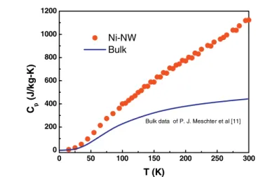
using Debye temperature θD and constant d as the only two adjustable fit parameters. As a result of the fitting we obtained the smaller value of θD = 440 K at fixed d than that is in case of the bulk (θD= 557 K). The reduction of the value of Debye temperature is presumably the reflection of softening of vibra-tion mode of nanowire compare to bulk sample due to enhanced disorder in nanowire. The reducvibra-tion of θD and softening of vibration mode have been observed previously for nanowires and disordered systems [8-10]. In particular, measurements of phonon density of states (DOS) of nanocrystalline Fe [9] and Ni3Fe [10] by means of inelastic nuclear scattering shows enlargement of low energy part of phonon DOS curve and smearing of high energy peak. Our obtained trend of Debye temperature and modifica-tion of the DOS of nanonocristalline materials are indicating that for this material the heat capacity can be enhanced compare to bulk samples. Figure 4 shows the measured heat capacity for our Ni nanowire. The heat capacity Cp behavior strongly differs from that of the bulk [11]. The temperature dependence of Cp at T>100 K comes close to the linear and the magnitude at room temperature exceed the bulk value 2.5 times. The additional specific heat may came from the contribution of lattice defects or grain bounda-ries which modify the phonon density of states as discussed above.
The magnetoresistance behaviour of Ni-NW is shown in Fig. 5, the behavior of magnetoresistance is likely due to the contributions of many effects which include Lorentz-MR, spin-dependent scattering, and anisotropic magnetoresistance (AMR). The MR-ratio calculated by formula (R(1T)-R(0))/R(0) is about 0.002. The smooth resistance decrease for H < Hc indicates a magnetization reversal process that incorporates a multidomain state of the magnetization. The peak value of magnetic field indicates that the coercive field is about 500Oe.
Fig. 3 The thermal conductivity (solid circles) of Ni-NW.Inset: the electrical resistivity (open circles) of Ni-NW and fitting curve (solid line).
3 3 3 3 ( ) ( ) ( ) ( ) , ( 1)(1 ) D E T i T x x D D T x dx T sd d d J e e T θ θ θ ρ θ - θ = = -
-Ú
0 50 100 150 200 250 300 0 5 10 15 20 25 0 100 200 300 20 30 40 ρ ( µΩ -c m ) T (K) Ni-NW BG formula The rm a l c onduc ti v it y ( W /m -K ) Temperature (K)0 50 100 150 200 250 300 0 200 400 600 Cp (J /k g T (K)
Bulk data of P. J. Meschter et al [11]
Fig. 4 The specific heat of Ni-NW and the bulk.
Fig. 5 The magnetoresistance of Ni-NW with magnetic field perpendicular to applied current.
4 Conclusion
The thermal conductivity (κ), specific heat (Cp) and the resistivity (ρ) of a single nickel nanowire (with dimensions of 35 µm x 180 nm x 100 nm.) have been measured in the temperature range from 4 to 300 K by means of the “self heating 3ω” technique. The temperature behaviour of the thermal conductivity of the nanowire is opposites to that of the bulk and decrease with temperature in the whole temperature range. An enhancement of specific heat ~250% of the bulk is also observed, which is presumably caused by softening of vibration mode of nanocrystalline Ni. In addition, the resistivity of nanowire at room temperature is about four times larger than that of the bulk. The small relative resistivity ratio (RRR) confirms the polycrystalline characteristic of the nanowire. The R(H) dependence of the nanowire at 0.5
-1.0 -0.5 0.0 0.5 1.0 342.3 342.4 342.5 342.6 342.7 342.8 342.9 343.0 343.1 Resistance ( Ω )
Magnetic Field (Tesla)
0 to 1 T 1 to -1 T -1 to 1 T 1 to 0 T Sample Temperature= 0.5 K I H
phys. stat. sol. (b) 244, No. 12 (2007) 4517 Paper
References
[1] M. Kawamura, N. Paul,V. Cherepanov, and B. Voigtlander, Phys. Rev. Lett. 91(9), 096102 (2003). [2] S. Mani, T. Saif, and J. H. Han, IEEE Trans. Nanotechnol. 5, 138 (2006).
[3] J. E. Wegrowe, D. Kelly, A. Franck, S. E. Gilbert, and J.-Ph. Ansermet, Phys. Rev. Lett. 82, 3681 (1999). [4] L. Lu, W. Yi, and D. L. Zhang, Rev. Sci. Instrum. 72(7), 2996 (2001).
[5] L. Piraux, M. Casssart, J. S. Jiang, J. Q. Xiao, and C. L.Chien, Phys. Rev. B 48, 638 (1993). [6] X. Y. Qin, W. Zhang, L. D. Zhang, L. D. Jiang, X. J. Liu, and D. Jin, Phys. Rev. B 56, 10596 (1997). [7] G. K. White and S. B. Wood, Phil. Trans. Royal Soc. 251(A995), 273 (1959).
[8] A. Bid, A. Bora, and A. K. Raychaudhuri, Phys. Rev. B 74, 035426 (2006).
[9] B. Fultz, C. C. Ahn, E. E. Alp, W. Sturhahn, and T. S. Toellner, Phys. Rev. Lett. 79, 937 (1997). [10] H. Frase and B. Fultz, Phys. Rev. B 57, 898 (1998).