國
立
交
通
大
學
電機學院 電子與光電學程
碩
士
論
文
利用大氣電漿對有機半導體
之介電層表面做改質研究
Modify Surface of dielectric layer on polymer thin-film
transistors by atmospheric-pressure Plasma technology
研 究 生:洪柏誠
指導教授:張國明 教授
利用大氣電漿對有機半導體
之介電層表面做改質研究
Modify Surface of dielectric layer on polymer thin-Film
transistors by atmospheric-pressure plasma technology
研 究 生:洪柏誠 Student:Hung Po Cheng 指導教授:張國明 Advisor:Kow-Ming Chang
國 立 交 通 大 學
電機學院 電子與光電學程
碩 士 論 文A Thesis
Submitted to College of Electrical and Computer Engineering National Chiao Tung University
in partial Fulfillment of the Requirements for the Degree of
Master of Science in
Electronics and Electro-Optical Engineering July 2011
Hsinchu, Taiwan, Republic of China
利用大氣電漿對有機半導體之介電層表面做改質研究 學生:洪柏誠 指導教授:張國明 博士 國 立 交 通 大 學 電 機 學 院 電 子 與 光 電 學 程 碩 士 班 摘 要 本論文研製之利用旋塗方式沉積有機薄膜電晶體對於元件製作有大面 積且低成本的好處。由於有機薄膜電晶體的效能跟半導體與介電層之間的 介面特性有很大的關係,所以此篇論文的研究目標是藉控制半導體與介電 層之間的化學特性,並呈現有機薄膜電晶體的改良特性。而因為二氧化矽 的製作及介面改質容易,在此我們選擇熱氧化方式的二氧化矽作為我們的 介電層。高規則度聚(3-烷基噻吩P3HT)具有較高的結晶排列特性,能夠提供 薄膜電晶體元件較高的電子遷移率,因此選用作為元件半導體層。經由六 甲基二矽氮烷的自組裝層所處理的氧化層介面, P3HT薄膜電晶體將獲得明 顯的改善。我們將使用常壓式電漿來實現介面處理。而常壓電漿系統是可 使用在大氣壓之下,同時製程溫度在 120 度以下。在本文可以看到這些表 面處理過後的電氣特性。處理過後的臨界電壓可被降至-9 伏特以內,載子 遷移率也由原先的 1.9×10⁻³ cm2 /Vs提升至 2.62×10⁻² cm2 /Vs。在本文中,可驗 證常壓式電漿系統,可提供低溫且高效率的有機薄膜電晶體介面改質製程。
Modify Surface of dielectric layer on polymer thin-Film
transistors by atmospheric-pressure plasma technology
student:Hung Po Cheng Advisors:Dr. Kow-Ming Chang
Degree Program of Electrical and Computer Engineering
National Chiao Tung University
ABSTRACTA procedure is usingthe spin coat way twists the organic thin film transistor can gain the advantage which is large area and lower cost in manufacturing. Because there is a close relations among the organic thin film transistor's potency, the semiconductor and the dielectric level's interface characteristic.
Therefore the research objective of the study is to present the improvement characteristic of the organic thin film transistor by the affiliation control semiconductor and the dielectric level chemical characteristic. And because the silicon dioxide manufacture and the interface change the nature is easy, we choose the thermal oxidization, the silicon dioxide, to be our dielectric level. High regioregularity poly(3-hexylthiophene) has the high crystallization arrangement characteristic, will provide the thin transistor part high electronic mobility, therefore it is selected to be the part semiconductor level. Through hexamethyldisilazane (HMDS) the oxide layer interface which will process from the assembly level institute, the P3HT thin film transistor will obtain the distinct improvement. We will use the to atmospheric-pressure plasma technology (APPT) to realize interface processing. And atmospheric-pressure plasma technology (APPT) can be used under the atmospheric pressure, simultaneous regulation temperature below 120 ℃. May see these surface treatment from now on electrical specification in this article. Processing from now on threshold voltage may drop to the - 9 volts, field-effect mobility also to promote by original 1.9×10⁻³cm2/Vs to 2.62×10⁻²cm2/Vs. That can confirm the atmospheric pressure plasma system, can provide the low temperature, and the high efficiency's organic thin film transistor interface to change the nature system regulation.
Acknowledgements 首先,我要感謝指導教授張國明老師,老師認真的教學精神和開明 的教學態度,使我這幾幾年研究生涯獲益匪淺,在此致上最深的謝意。 謝謝黃士軒學長在碩士班幾年間給予我的建議及協助,使我的實驗 能順利完成。也要謝謝張庭嘉學長、黃菘宏學長、林志祥學長、呂成家 同學,有了他們的協助及指導,使得研究能夠更加完整。 感謝我的口試委員:王水進老師、鄧一中老師、吳建宏老師,由於 你們的指導,使我的論文內容更加完備。 感謝所有指導過我的老師,學長,同學,雖然我們相識不久,但是 你們的熱情,讓我感覺到交通大學這個大家庭,是充滿溫暖的,不單單 只是求學的地方。 謝謝交大奈米中心、國家奈米實驗室提供各種機台設備,讓我可以 進行實驗;同時感謝所有工程師的技術指導。 最後,更感謝我的父母,洪建和先生與吳英祝女士,感謝他們對我 從小到大的養育及栽培,在生活上給我無微不至的關心,讓我得以全心 完成學業。我相信他們會以我為榮。
Contents Chinese Abstract i English Abstract ii Acknowledgements iii Contents iv Table Captions vi
Figure Captions vii
Chapter 1 Introduction 1
1.1General Background and Motivation 1
1.2Thesis Organization 3 Chapter 2 Property of P3HT 6 2.1 Introduction of Poly(3-hexylthiophene) P3HT 6 2.1.1 P3HT molecular structure 6 2.1.2 Conduction Mechanism 7 2.1.3 P3HT alignment 8
2.2 Solution processed deposition 9
2.2.1 OTFT method manufacture 9
2.2.2 The Motivation for Spin-Coat 10
2.2.3 Polymer morphology and resolver function 11
2.3 Contact Resistance of P3HT OTFT 12
2.4 Operation of Organic Thin Film Transistors 13
Chapter 3 Influence of APPT for OTFT 24
3.1 Oxide compound surface revision 24
3.2 Introduction of APPT 25
3.2.1 Introduction of plasma 25
3.2.2 Applications of APPT 26
3.2.3 Surface modification by plasma 27
3.3 Fabrication of OTFT 30
3.4 Determination of Thershold voltage and Mobility 31
3.5Results and discussion 31
3.5.1 The influence of APPT 32
3.5.3 Hysteresis 35
3.5.4 Anomalous leakage 37
3.5.5 Crystallization behavior of P3HT 37
3.5.6 XRD and UV-vis for highly oriented crystals of P3HT 38
Chapter 4 Conclusions and Future work 77
4.1 Conclusions 79
4.2 Future work 81
4.2.1 In-situ passivation layer for protecting the P3HT film 81
4.2.2 Novel method for depositing P3HT thin films 82
4.2.3 Thermal stability of P3HT OTFT 82
4.2.4 Use APPT Grows SiO2 and the surface treatment 82
Table Captions Chapter 1
Table1-1 Highest field-effect mobility (μ) values measured from OTFT as reported in
the literature annually from 1986 through 2000[12].
Chapter 2
Table 2-1:Field-effect mobility and ON/OFF ratio of samples prepared from different
solvents and process condition [14]. Condition 1, cast , vacuum pumped for 24 h; condition 2, spin-coated; condition 3, treated with NH3 for 10 h;
condition 4, heated to 100 ℃ under N2 for 5 min; condition 5, heated to 150
℃ under N2 for 35 min. Chapter 3
Table 3-1:Electrical parameters of the OTFTs in this study.
Table 3-2:Comparison of contact angle and surface roughness with
different scanning times by APPT
Table 3-3:The different methods of surface treatment Table 3-4:The different methods of surface treatment
Table 3-5:Tm and △H of P3HT in Run first and second time with difference pre-heating
temperature.
Figure Captions Chapter 1
Figure1-1:Semilogarithmic plot of the highest field-effect mobility(μ)
Reported for OTFT fabricated from the most promising polymeric and oligomeric semiconductors versus year from 1986 to 2000[12]
Chapter 2
Figure 2-1:The structure of the polymer chain of P3HT
Figure 2-2:Two different orientations of ordered P3HT (a)Edge-on orientation
(b)Face-on orientation
Figure 2-3:The molecular structure of P3HT s for High RR (d100b-band d100b-b are the
a-direction and b-direction chain-stacking spacings, respectively)The
a-direction and b-direction are parallel and perpendicular to the thiophene ring plane, respectively (see the chemical structures within the ovals as well asthe schematic illustration for lamella folding and ordering on a substrate).
Figure 2-4:(a) charge carrier transport in conjugated polymers(b) charge transport
mechanisms in solid
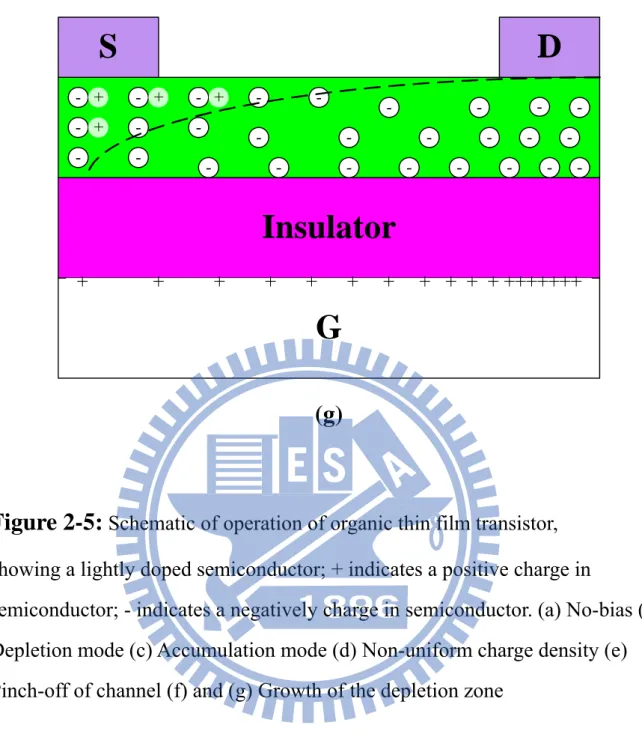
Figure 2-5:Schematic of operation of organic thin film transistor, showing a lightly
doped semiconductor; + indicates a positive charge in semiconductor; - indicates a negatively charge in semiconductor. (a) No-bias (b) Depletion mode (c) Accumulation mode (d) Non-uniform charge density (e) Pinch-off of channel (f) and (g) Growth of the depletion zone
Chapter 3
Figure 3-1:(a)The structure of APPT (b)The diagram of plasma surface treatment Figure 3-2:(a) APP system of ITRI (b) The other APP systems
Figure 3-3:Two basic structures of OTFT Figure 3-4:Process flow of top-contact OTFT
Figure 3-5:Surface treatment of APPT HMDS 1 for OTFT(a) ID-VG curve and (b) ID-VD
curve(W/L = 2000 um/500 um)
Figure 3-6: Surface treatment of APPT HMDS 2 for OTFT(a) ID-VG curve and(b) ID-VD
curve(W/L = 2000 um/500 um)
Figure 3-7:Surface treatment of APPT HMDS 4 for OTFT(a) ID-VG curve and(b) ID-VD
Figure 3-8:Surface treatment of APPT HMDS 8 for OTFT(a) ID-VG curve (b) ID-VD
curve (W/L = 2000 um/500 um)
Figure 3-9 :The comparison of (a), (b) ID-VG and (c), (d) ID-VD with different scanning
times by APPT
Figure 3-10:Comparison of threshold voltage and saturation mobility with different
scanning times by APPT
Figure 3-11:Contact angle vs. different scanning times by APPT
Figure 3-12:Contact angle of (a) No treatment (<10°) (b) APP1(68.9°) (c) APP2 (76.3°)
(d) APP4 (90.5°) (e) APP8 (90.9°)
Figure 3-13:AFM micrography of (a) No treatment (b) APP1 (c) APP2 (d) APP4
(e)APP8
Figure 3-14: (a) ID-VG curve and(b) ID-VD curve with spin-coating HMDS for OTFT Figure 3-15: (a) ID-VG curve and(b) ID-VD curve with evaporated HMDS for OTFT Figure 3-16:Comparison of threshold voltage and saturation mobility with different
methods of surface treatment
Figure 3-17:Contact angle of (a) spin-coating HMDS (65.49°) and(b) evaporated HMDS
(75.28°)
Figure 3-18:AFM photography of (a) Spin-coating HMDS and(b) evaporated HMDS Figure 3-19:The comparison of (a), (b) ID-VG and (c), (d) ID-VD with different methods
of surface treatment
Figure 3-20 Comparison of contact angle and surface roughness with different methods of
surface treatment
Figure 3-21 Comparison of surface roughness and mobility with different methods of
surface treatment.
Figure 3-22:Comparison of contact angle and mobility with different methods of surface
treatment and different scanning times by APPT
Figure 3-23:Comparison of contact angle and roughness with different methods of surface
treatment and different scanning times by APPT.
Figure 3-24:Comparison of roughness and mobility with different methods of surface
treatment and different scanning times by APPT.
Figure 3-25: A typical hysteresis curve.
Figure 3-26:Hysteresis of P3HT OTFTs with no surface treatment.
Figure 3-28:Hysteresis of P3HT OTFTs with evaporation surface treatment. Figure 3-29:Hysteresis of P3HT OTFTs with APP 1 times surface treatment. Figure 3-30:Hysteresis of P3HT OTFTs with APP 2 times surface treatment. Figure 3-31:Hysteresis of P3HT OTFTs with APP 4 times surface treatment. Figure 3-32:Hysteresis of P3HT OTFTs with APP 8 times surface treatment.
Figure 3-33:ID versus VG for various surface treatment processes and the gate leakage
currents in VG approaches 0 V.
Figure 3-34:ID versus VG for different numbers of APP scans and the gate leakage
currents in VG approaches 0 V.
Figure 3-35:TGA thermograph of P3HT. 5 % weight loss is about 500℃.
Figure 3-36:DSC thermograph of P3HT was pre-heating at the temperature of 70℃ for 3
min.
Figure 3-37:DSC thermograph of P3HT was pre-heating at the temperature of 90 ℃ for 3
min.
Figure 3-38:DSC thermograph of P3HT was pre-heating at the temperature of 110 ℃ for
3 min.
Figure 3-39:DSC thermograph of P3HT was pre-heating at the temperature of 130 ℃ for
3 min.
Figure 3-40: DSC thermograph of P3HT was pre-heating at the temperature of 150 ℃ for
3 min.
Figure 3-41:Tm and △H of P3HT in Run first time with difference pre-heating
temperature.
Figure 3-42:Tm and △H of P3HT in Run second time with difference pre-heating
temperature.
Figure 3-43:X-ray analysis of deposition of P3HT on SiO2 dielectric layer with various
surface treatments.
Figure 3-44:UV-VIS absorption spectra of P3HT films that are deposited on SiO2 dielectric
layers following various surface treatments, normalized to the maxima of the spectra.
Chapter 1
Introduction
1.1General Background and Motivation
In the last few years, Today’s microelectronics is based on the use of highly pure and high performance semiconductors like Si, Ge, GaAs, and InP, etc. These materials can provide carrier mobility (μ) in the order 103 cm2/Vs at room temperature, offer long lifetime, can be precisely doped and patterned with accuracy better than 100 nm. In this way, they profit at best of the device speed and manufacture complex systems on chip that are capable to receive, memorize, elaborate and transmit enormous quantity of information, making possible like PCs, mobile phones and almost every commercial products around our daily life.
Organic thin-film transistors (OTFT) using organic semiconductors have attracted a great deal of interest for use in lightweight, low-cost, large-area and flexible electronic products such as flat-panel displays, sensors, smart cards, and radio-frequency identification (RFID) tags. OTFT are more compatible with polymeric substrates than conventional silicon-based transistors because they can fabricated with a low-temperature process. Therefore, OTFT on polymeric substrates have been developed to construct organic integrated circuits [1,2,3], electric papers, active-matrix liquid crystal displays (AMLCDs) [4,5], and active matrix organic electroluminescent displays [6].
Organic thin-film transistors (OTFT) based on conjugated polymers, oligomers, or other molecules have been envisioned as a viable alternative to more traditional, mainstream thin-film transistors (TFT) based on inorganic
materials. Because of the relatively low mobility of the organic semiconductor layers, OTFT can’t rival the performance of field-effect transistors based on single-crystalline inorganic semiconductors, such as Si, Ge, GaAs, and InP, which have charge carrier mobilities about three orders of magnitude higher [7].
The performance of OTFT has steadily improved in the last two decades as a result of the development of new organic semiconductors, the optimization of deposition conditions and gate dielectric surface treatments [8,9,10,11]. We presented a semilogarithmic plot of the highest yearly reported field-effect mobility value measured from thin-film transistors based on specific organic semiconductors, beginning in 1986. An update of that plot is showen in Figure 1-1, which is based on Table 1-1.
Solution-processable conjugated polymers are among the most promising candidates for a cheap electronic and optoelectronic technology on plastic substrates. The technology that is believed to have the potential to produce the highest impact on manufacturing costs is the use of soluble organic semiconductor, both polymers and oligomers, combined with large area coating employed in OTFT is the fact that can be deposited using very low cost procedures such as spin-coating. This is the case of soluble polymers such as regioregular polythiophenes we used in experiments. Spin-coating procedures are also thermally compatible with plastic substrates, because they are carried out at the room temperature.
Therefore, here we employ the poly-3-hexylthiophene (P3HT), solution
processable conjugated materials, as active layers in OTFT. Atmospheric- pressure plasma technology (APPT) will be adopted to treat the surface of dielectric of OTFT and discuss the influence.
1.2 Thesis Organization
In chapter 1, we describe our background and motivation of our study.
In chapter 2, we will introduce the characteristic of P3HT and methods for OTFT
fabrication.
In chapter 3, we adopt a new process, APPT, whcih can be operated under low temperature and atmospheric ambient. And APPT will make use of modify surface of dielectric layer SiO2 for our experimet. In addition, the other methods
of HMDS surface treatment will also be utilized in our experment. we compare the various methods of surface treatment and
use DSC XRD and UV-VIS to
demonstrate that highmobility requires an ordered structure. And we also
explain that the phenomenon of the hysteresis behavior and the anomalous
leakage current of OTFT device
discuss the results.Figure1-1
: Semilogarithmic plot of the highest field-effect mobility(μ)Reported for OTFT fabricated from the most promising polymeric and oligomeric semiconductors versus year from 1986 to 2000 [12]
Table1-1
Highest field-effect mobility(μ) values measured from OTFT as reported in the literature annually from 1986 through 2000 [12].Chapter 2
Property of P
3HT
2.1 Introduction of Poly(3-hexylthiophene) P
3HT
2.1.1 P
3HT molecular structure
The field-effect mobility of P(3-hexylthiophene) P3HT is strongly
influenced by the structure of the polymer chain and the direction of intermolecular π-π stacking. The structure of the polymer chain of P3HT is
shown in Fig 2-1 . The 3-alkylsubstituents can be incorporated into a polymer chain with two different regioregularities: head to tail (HT) and head to head (HH) [13,14].
R represents the alkyl side chain(C6H13 for P3HT), which allows P3HT to be
dissolved in solvents like chloroform. This solution processability enables simple film deposition. A regiorandom P3HT consists of both HH and HT
3-hexylthiophene in a random pattern while a regioregular has only one kind of 3-hexylthiophene, either HH and HT. This type of order is known as regioregularity and has been shown to give much higher field-effect mobility values over regiorandom material [15]. In our experiments, regioregular P3HT
(HT regioregularity of 98.5%) and high grade solvent, chloroform, were purchased from Aldrich Chemical Company. A dramatic increase in mobility was observed relative to regiorandom poly-3-alkylthiophenes [16] when regioregular P3HT consisting of 98.5% head to tail(HT) linkages, so we did not
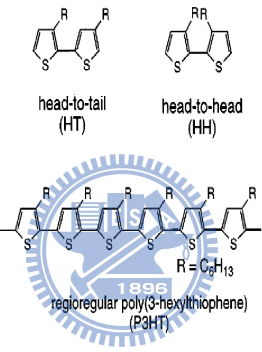
perform further purification to these chemicals in our experiments. After being deposited on the substrate, P3HT backbones may form two different
morphologies, edge-on or face-on of lamella structure as shown in Fig 2-2. The higher mobility is given by edge-on structure since the carriers can move more efficiently through intra-chain transport along the direction ofπ-π stacking. Two different methods are applied to deposit the P3HT film, one is spin-coating
and while the other is dip-casting. The mobility of dip-coated films is usually higher than that of the spin-coating that’s maybe due to the evaporation rate of solvents. Lower evaporation rate results in a slower crystal growth with better ordered polymer structure [16,17]. In spite of that method provide the higher field effect mobility, the dip-coating method can not be applied for coverge of a large area. Therefore, in all of our experiments, we used spin-coating technique as a key process of organic layer deposition.
2.1.2 Conduction Mechanism
The weak intermolecular interaction forces in organic semiconductors, most usually van der Waals interactions with energies smaller than 10 Kcal mol-1, may be responsible for such small carriers mobility. In contrast, in inorganic semiconductors such as Si and Ge, the atoms are tied together with very strong covalent bonds, which for the case of Si have energies as high as 76 Kcal mol-1. In these semiconductors, charge carrier flows like highly delocalized plane waves in the wide bands and have very high mobility. On the other hand, inorganic semiconductors usually have high order lattice structures and there are fewer traps than organic ones. This is another reason to explain the poor electrical characteristics of organic electronics.
However, for conjugated organic materials, the polymer chains are weakly bound by van der Waals force. These polymer typically have narrow energy bands, highest occupied molecular orbit (HOMO) and lowest occupied molecular orbit (LOMO), which can easily be disrupted by disorder. Due to disorder structures, band transport is not applicable to organic semiconductors; in which carrier transport take place by hopping[18] between localized state like Fig 2-4. Transport from one molecular to another is much more difficult due to a small energetic coupling between molecules held by weak van der Waals force of~10 Kcal mol-1.Another characteristic of organic material is that most polymers conduct one kind of carrier only, either electron or hole(P3HT is p-type
that majority carriers are holes). Because of the nature of large band gap(e.q. Eg of P3HT = 2.2 eV), the active layer cannot be inversed by thermal energy at
room temperature(i.e. solw generation rate of inversion layer). Therefore, OTFTs operate in the accumulation mode at it’s ON state and depletion at it’s OFF state.
P3HT are semi-crystalline in nature, and their conduction mechanism is
complex. The crystalline portion can conduct through intra-chain and inter-chain transport, whereas the amorphous portion conducts current through hopping processes.
2.1.3 P
3HT alignment
3-Alkyl substituents can be incorporated into the poly(3-hexylthiophene) polymer in two arrangements (Fig.2-1) - head to tail (HT) and head to head(HH).A regiorandom P3HT has both HH and HT 3-hexylthiophenes in a random pattern
Structure-controlled syntheses of P3HT have been recently developed, and
regioregular P3HT with HT linkages of greater than 98.5% can be obtained
[19,20]. Most interestingly, these polymers have been shown to have very different properties from their corresponding regiorandom polymers, such as smaller band gaps, better ordering and crystallinity in their solid state, as well as markedly improved electroconductivities. Highly regioregular P3HT self-orients into a
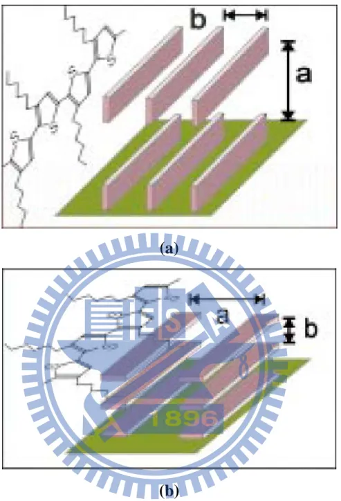
well-ordered lamellar structure with an edge-on orientation of the thiophene rings relative to the substrate. In samples with a high regioregularity (>91%), the preferential orientation of ordered domains is with the (100)-axis normal to the film and the(010)-axis in the plane of the film (Figs. 2-2 and 2-3). In contrast, low regioregularity (81% head-to-tail linkages) is associated with lamellae with a face-on orientation, and crystallites that are preferentially oriented along the (100)-axis in the plane and the (010)-axis normal to the film. In another work [21], Prosa et al. presented the different intensity distributions of the (100) reflections that are associated with the lamella layer structure and the (010)reflections that are associated with π - π interchain stacking. Therefore, in this study, highly regioregular (98.5%) P3HT is adopted as the active layer, and the above
characteristics are exploited to provide P3HT alignment.
2.2 Solution processed deposition
2.2.1 OTFT method manufacture
There are four methods to form organic semiconductor film: (1) solution-processed deposition, (2) electro-polymerization, (3) vacuum
evaporation, and(4)Langmuir-Blodgett Technique [22]. Recently, many researchers extensively use solution-processed deposition to fabricate organic semiconductor film. For solution-deposited organic semiconductor film, one kind of the organic semiconductor material such as poly (3-hexylthiophene) are dissolved in solvent such as chloroform. In our experiment, we use P3HT as the
semiconductor because P3HT has many potential advantages for use the
semiconductor layer in field-effect transistors. (1) P3HT is a well-knowen
polymer as an organic semiconductor and has shown the effect mobility from 10-4 cm2/Vs in 1988 to 0.2 cm2/Vs in 2003. [12,23]. (2) P3HT has high solvent
selectiveness, can dissolve in toluene, xylene, chloroform and so on. (3) P3HT is
solution processed, therefore can be processed by spin-coating .
2.2.2 The Motivation of Spin-Coat
The organic semiconductors that exhibit the best mobility, ON/OFF Current ratio,uniformity over large areas, and devices reproducibility have been deposited by vacuum sublimation. However the need for expensive vacuum chambers and lengthy pump-down cycles is unavoidable. Since the organic semiconductors have the relativity low mobility of organic semiconductors as described in chapter 1, OTFT cannot rival the performance of based on single crystalline inorganic semiconductors, such as Si, Ge, and GaAs. However, the unique processing characteristics and demonstrated performance of OTFT suggest that they can be competitive candidates for existing or novel thin film transistor applications requiring large area coverage, structural flexibility, low temperature processing, and especially low cost. Some recent efforts in the field have focused on processes for solution deposition of small molecule [24] and
polymers, as well as integration of these process with other non-lithographic device fabrication technique [25]. To realize truly the advantages (i.e., processability and low cost) of organic materials in device applications, liquid phase processing technique by spin-coating is strongly desired. In all of our experiments, we used spin-coating technique as a key process of organic layer fabrication.
2.2.3 Polymer morphology and resolver function
The molecular structure of the P3HT greatly influences the charge carrier
mobility and related current-voltage (I-V) characteristics of OTFT.
A comparison study of P3AT (A = hexyl, octyl, dodecyl, hexadecy) with side chains ranging from butyl to decyl showed that field-effect mobility decreases with increasing chain length [26].
Under different processing conditions, the field effect mobility of OTFT is highly anisotropic. For example, Karl et al [27] observed that the field effect mobility was highly anisotropic, with the larger mobility along the direction in which the polymer chain axis aligned.
The molecular structure obtained by using spin-coating films is usually lower than that of the cast films [16]. This is perhabs because in the cast films, the rate of solvent evaporation is slower and has slower crystal growth, and hence better ordering, and large grain size.
The choice of solvents and polymers has a very significant impact on the electrical characteristics of OTFT. In a recent publication, Bao et al [18]. Observed that when chloroform was used as a solvent to make poly -(3-hexylthiophene)-based transistors, the field-effect mobility was 0.1 cm2Vs-1.
However when Tetra hydrofuran (THF) was used as the solvent, the value of field-effect mobility is only 0.0006 cm2Vs-1. Table 2-1 shows the performance of various devices made from casting poly(3-hexylthiophene) films using different solvents with different process conditions [14].
Sirringhaus et al., [18] observed that the mobility could differ by a factor of 100 depending on the direction ofπ-π stacking in which efficient inter-chain transport is happened . The polymer solution we used is regioregular P3HT in
chloroform with high purity. From Table 2-1, the mobility is typically in the range 10-3 which matches the result obtained in our experiment.
2.3 Contact Resistance of P
3HT OTFT
There are many parameters will impact the performance of OTFT. The contact resistance between the source/drain electrodes and the organic semiconductor is an important one of them [28-30]. The contact resistance between the source/drain electrodes and the semiconductor becomes increasingly important to device performance. The contact resistance dominates the overall device resistance.
Material of source/drain electrodes and the structure both affect the contact characteristics between the source/drain electrode and the organic semiconductors. Unlike the FET of single-crystalline silicon, polycrystalline silicon, or hydrogenated amorphous silicon, the P3HT material cannot be
optimized easily by semiconductor doping or silicide formation. Such properties of organic semiconductors deteriorate the performance of devices; moreover, the chemical compound always increase the contact resistance between the source/drain electrode and the organic semiconductor [31,32]. It is a
straightforward method to find a suitable electrode material which forms ohmic contact with the organic active layer and thus to improve the performance of OTFT. P3HT can form an ohmic contact with material for its work function
larger than 4.5eV because the work function of P3HT is 4.5eV. Work functions
of all materials we used are larger than 4.5eV; they include Ni(5.1eV), Pt(5.65eV),and Cr(4.5eV).
2.4 Operation of Organic Thin Film Transistors
Refer to [33], the operation of the P3HT which bases on OTFT is described
below. Organic thin-film transistors are opposed to the usual inversion mode operation of silicon MOSFETs and primarily operated as a P-type accumulation-mode enhancement type transistor. There are four basic modes which will be described later.
Mode (I): When zero bias is applied to three electrodes of OTFT. The schematic diagram is shown in Fig 2-5(a), it is called cut-off. If applied a small drain bias, Vd, and the source-current, Ids, will be small and ohmic.
Mode (II): When a positive bias applied, the bend bending will occur in the interface between dielectric layer and semiconductor layer. Negative charges will locate at interface and form the depletion region. The schematic diagram is shown in Fig 2-5(b). The channel resistance is so large that the current will smaller than that of mode (I). Because of the large band gap, inversion layer cannot be observed in the organic thin-film transistor.
Mode (III): When gate bias is negative, the schematic diagram is shown in Fig 2-5(c), the voltage is dropped over the insulator and over the semiconductor near the interface between dielectric layer and semiconductor layer. More
positive charges will be accumulated in the accumulate region. When a small bias is applied to drain, the source-drain current will be larger than that of Mode (I), the schematic diagram is shown in Fig 2-5(d).
Mode (IV): When drain voltage is negative enough that the voltage difference of gate and drain, Vgd, which is lower than Vth(<0), therefore, the depletion region will form near drain and pitch-off (Fig 2-5(e)). If drain voltage is more negative, the depletion region will grow and approach source. The schematic diagram is shown in Fig 2-5(f)(g).
(a)
(b)
Figure 2-2:
Two different orientations of ordered P3HTFigure 2-3
: The molecular structure of P3HT s for High RR (d100b-bandd
100b-bare the a-direction and b-direction chain-stacking spacings,
respectively)The a-direction and b-direction are parallel and perpendicular to
the thiophene ring plane, respectively (see the chemical structures within the
ovals as well asthe schematic illustration for lamella folding and ordering on
a substrate).
(a)
(b)
Figure 2-4:
(a) charge carrier transport in conjugated polymers andTable 2-1:
Field-effect mobility and ON/OFF ratio of samples prepared from different solvents and process condition [14].Condition 1, cast , vacuumpumped for 24 h; condition 2, spin-coated; condition 3, treated with NH3 for 10
h; condition 4, heated to 100 ℃ under N2 for 5 min; condition 5, heated to 150
℃ under N2 for 35 min.
.
G
Insulator
S
D
-+ + + + + + + + + + + + + + + + + + + + + + + + + + +(a)
V
S= V
D= 0, V
G> 0
G
Insulator
S
D
-+ + + + + + + + + + + + + + + + + + -+ -+ -+ -+ -+ -+ -+ -+ -+ -+ -+ -+ -+ -+ -+ -+ -+ -+ -+ -+ -+ -+ -+ -+ -+ -+ -+ -+ -+ -+ -+ -+ +(b)
V
S= V
D= 0, V
G< 0
G
Insulator
S
D
-- - -+ + + + + + + + + + + + + + + + + + + + + + + + + + + + + + + + + + + + + + + + + + + + + + + + + + + - - - -(c)
V
S=0, V
G< V
D< 0
G
Insulator
S
D
-- - -+ + + + + + + + + + + + + + + + + + + + + + + + + + + + + + + + + + + + + + - - - - - - - - - - - -(d)
V
S=0, V
D< V
G< 0
G
Insulator
S
D
-+ + + + + + + + + + + + + + + +++++ + + + + + + + + + + + --- - - - - - - - - - - - + + + + +++++ -- - - ---(e)
V
S= V
G= 0, V
D< 0
G
Insulator
S
D
-- - -+ + + + + + + + + + + + + + + + + + + + +++++++ -- - - -- -- - --(f)
V
S= V
G= 0, V
D<< 0
G
Insulator
S
D
-- - -+ + + + + + + + + + + + + + + +++++++ -- - - -- -- - --(g)
Figure 2-5:
Schematic of operation of organic thin film transistor,showing a lightly doped semiconductor; + indicates a positive charge in
semiconductor; - indicates a negatively charge in semiconductor. (a) No-bias (b) Depletion mode (c) Accumulation mode (d) Non-uniform charge density (e) Pinch-off of channel (f) and (g) Growth of the depletion zone
Influence of APPT for OTFT
3.1 Oxide compound surface revision
The interface between an organic material and dielectric layer is a critical factor for device performance. This is because the surface of the dielectric strongly influences the quality of the dielectric/channel interface and the crystalline organic channel. The quality of the interface and the organic channel, as well as the electrical properties of the gate dielectric itself, play a major role in determining the device performance of an OTFT [34-36]. Although several methods have been recently proposed to improve the condition of the interface states, only a few have been proved to be reliable and robust. One of the proposed methods is the use of a self-assembly monolayer (SAM), such as octadecyltrichlorosilane (OTS) [37] and hexamethyldisilazane (HMDS) [38],have been extensively studied. A dielectric surface treatment with OTS is found to improve the mobility of OTFTs. Another dielectric surface treatment technique is O2 plasma cleaning and
subsequent HMDS deposition on dielectrics [38]. A problem owing to O2 plasma
cleaning, which is applied to remove residues generated from previous photolithography processes, was found to be the generation of a large number of trap states during the cleaning process by assisting OH termination at the SiO2
surface [39]. Although a HMDS layer subsequently applied is expected to reduce the number of traps and act as a SAM, the time-consuming wet processes used to apply a SAM on the interface are unreliable and can cause other undesirable contaminations of the device. Surface treatments using an ion beam have been widely studied in other research fields. It is well known that ion implantation techniques can change the surface conditions or thin-film properties [40]. In
the
LCD fabrication process, for example, Ar ion beam treatment has been
considered as a viable option as a surface treatment method to replace
conventional contact-based treatment such as rubbing [41]. One of the
advantages of Ar ion beam treatment is that because argon is an inert gas, it
can clean the surface effectively without affecting the chemical structure of
the dielectric layer.
3.2 Introduction of APPT
3.2.1 Introduction of plasma
Plasma can be defined as a partially or wholly ionized gas with a roughly equal number of positively and negatively charged particles. Some scientists have dubbed plasma the "fourth state of matter" because while plasma is neither gas nor liquid, its properties are similar to those of both gases and liquids.
There are two types of plasma - high temperature and low temperature. A good example of naturally occurring high temperature plasma is lightning. This type of plasma can be artificially generated using a high voltage, high temperature arc, which is the basis for the corona discharge process and for the plasma torch used to vaporize and redeposit metals. Low temperature plasmas, used in surface modification and organic cleaning, are ionized gases generated at pressures between 0.1 and 2 torr. These types of plasmas work within a vacuum chamber where atmospheric gases have been evacuated typically below 0.1 torr. Low pressure allows for a relatively long free path of accelerated electrons and ions. Since the ions and neutral particles are at or near ambient temperatures and the long free path of electrons, which are at high temperature or electron volt
levels, have relatively few collisions with molecules at this pressure the reaction remains at low temperature.
3.2.2 Applications of APPT
Therefore this has been occupied for several years with developing atmospheric pressure plasma processes for surface coating and treatment. Table 3-1 shows the type of atmospheric pressure plasma.
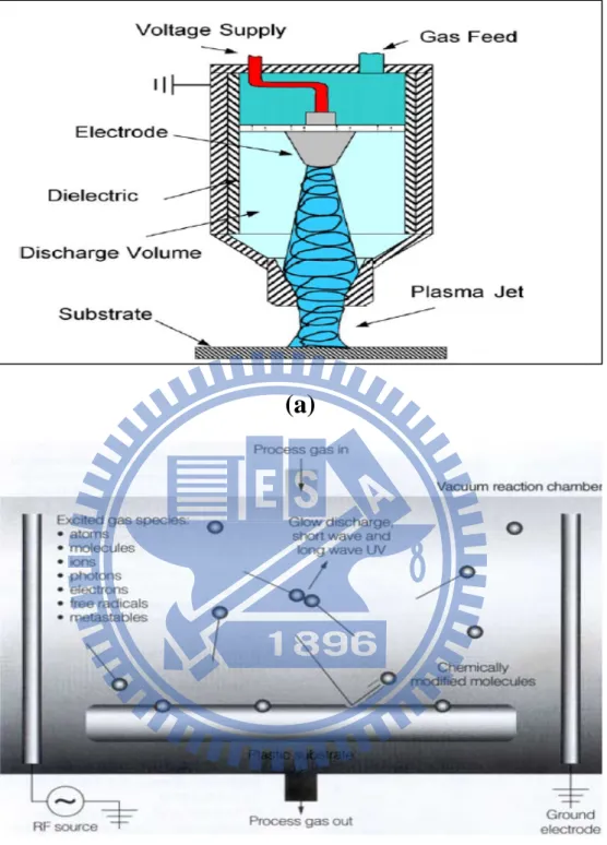
Atmospheric pressure plasma is particularly suited for the large-area surface treatment of flat substrates (Fig. 3-1). This forms between two electrodes on application of an alternating current if at least one dielectric barrier or insulator obstructs the current. Gases are activated in these micro discharges by electronic excitation, ionization and dissociation to form very chemically reactive species. Thus the average gas temperature in the discharge gap rises only a few degrees Kelvin. Since the discharge in effect remains "cold" even temperature-sensitive substrates can be treated. Despite the filament of the discharge, with appropriate process control it is normal to achieve a very uniform surface treatment.
The atmospheric-pressure plasma technology (APPT) is useful for treating and modifying the surface properties of organic and inorganic materials. The APT apparatus does not require any vacuum systems, produces a high density plasma, and provides treatment of various substrates at low temperatures while operating open to the atmosphere. The plasma system has used for a wide variety of applications including treatment of polymer films, paper, wood, and foils; plasma grafting and plasma polymerization; ash various materials in the microelectronics industry; barrier layer deposition for the packaging industry;
and sterilizing biologically contaminated materials. For polymer films, the technique offers the following advantages:
• Uniform treatment and No backside treatment.
• Improved surface energy with concomitant improved wettability, printability, and adhesion
• No additional vacuum system and low cost
• Continuous fabrication availably and high speed for production • High plasma density
As shown in Fig 3-1(a), we exhibited the atmospheric-pressure plasma system which was used in our experiment, and also showed the other atmospheric -pressure plasma systems in Fig 3-1(b).
3.2.3 Surface modification by plsama
Fig 3-2 shows the mechanisms of plasma surface modification, a glow discharge plasma is created by evacuating a reaction chamber and then refilling it with a low-pressure gas. The gas is then energized by one of the following types of energy: radio frequency, microwaves, and alternating or direct current. The energetic species in gas plasma include ions, electrons, radicals, metastables, and photons in the short-wave ultraviolet (UV) range. Surfaces in contact with the gas plasma are bombarded by these energetic species and their energy is transferred from the plasma to the solid. These energy transfers are dissipated within the solid by a variety of chemical and physical processes to result in a unique type of surface modification that reacts with surfaces in depths from
several hundred angstroms to 10µm without changing the bulk properties of the material.
A wide variety of parameters can greatly affect the physical characteristics of the plasma and subsequently affect the surface chemistry obtained by plasma modification. Processing parameters, such as gas types, treatment power, treatment time and operating pressure, can be varied by the user; however system parameters, such as electrode location, reactor design, gas inlets and vacuum are set by the design of the plasma equipment. This broad range of parameters offers greater control over the plasma process than that offered by most high-energy radiation processes.
Plasma treatment is aiming for various goals as for example:
• Improved adhesion
• Removal of the "water skin" • Activation of the substrate surface • Modification of the substrate surface • Cleaning of substrate surfaces
Since the organic film of OTFT is fabricated on to the dielectric layer under the influence of the physical and chemical interactions between organic and dielectric layer, the OTFT performance strongly depends on the semiconductor /dielectric interface. The purpose of this work is to show the improvement of OTFT performance by controlling the surface treatments of dielectric/polymer interface. The surface properties such as frictional or abrasion, permeability, insulating properties, wettability and chemical reactivity are strongly dependent on a molecular aggregation state of the surface [33,34]. Therefore, the control of
a molecular aggregation state in the film is important to construct a highly functionalized surface. One of the most effective ways of studying surface properties is contact angle measurement. The contact angle is the angle between the tangent to the drop’s profile and the tangent to the surface at the interaction of the vapor, the liquid, and the solid. The contact angle is an index of the wettability of the solid surface. A low contact angle between solid surface water-drop indicates that the surface is hydrophilic and has a high surface energy. On the contrary, a high contact angle means that the surface is hydrophobic and has a low surface energy. The surface free energy was traditionally quantified by contact angle measurements [42,43]. In our work, we investigated the electrical properties of the OTFT using by APPT. Hexamethyldisilasane ((CH3)3-Si-O-Si-(CH3)3) (HMDS) have already been
widely used for oxide-based dielectric [45]. Oxide surfaces were treated with hexamethyldilazane to improve the adhesion between polymer chain and oxide surfaces. Modification of the substrate surface prior to deposition of regioregular P3HT has also been found to influence film morphology.For example, treatment
of SiO2 with hexamethyldilazane (HMDS) or an alkyltrichlorosilane replaces the
hydroxyl groups at the SiO2 surface with methyl or alkyl groups. The apolar
nature of these groups apparently attracts the hexyl side chains of P3HT,
favoring lamellae with an edge-on orientation [18]. According to [18], the mobility of OTFT with an edge-on orientation P3HT film is higher than the one
with a face-on orientation.
And so HMDS would be adopted in our experiment. We will discuss and analyze the effects of APPT surface treatments latter, and find the optimum parameters in our experiments.
3.3 Fabrication of OTFT
There are two kinds of basic structures which are adopted generally, bottom contact (BC) and top contact (TC) were shown in Fig 3-3.
Top-contact device is favorable compared to deposition onto prefabricated source and drain electrodes bottom-contact device, yielding mobilities that are typically larger by a factor of 2 [45,46].
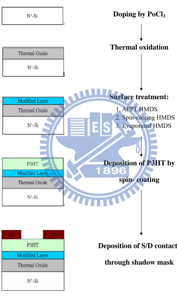
First, an n-type bare silicon wafer was cleaned by the standard RCA cleaning process. After that, phosphorous atoms were diffused into an n-type silicon wafer by POCl3 to form a common gate electrode. We used dilute HF to remove
SiO2 after diffusing. Before the insulating layer of silicon dioxide was deposited,
the n+ silicon wafer must be cleaned by the standard RCA cleaning again. An insulating layer of silicon dioxide was grown by thermal oxidation 5hr at 1000
℃
. The thickness of silicon dioxide was 200nm measured by n&k system. The wafers was taken to remove silicon dioxide of backside, then gate dielectric layer was formed. The “top-contact” OTFT structures were treated by different surface treatments before deposition of the P3HT active layer. The surfacetreatments were to control chemical and physical characteristics of surface by different ways. In our experiments, we adopted three methods of surface treatments and compared the difference of them.
(1) Spin-coating HMDS adopted at 800rpm for 3 sec as step one, 1500 rpm for 35 sec as step two, and baking at 150℃ for 30 min.
(2) Evaporated HMDS at 150℃
(3) Atmospheric pressure plasma technology (APPT) was operated at 50W of plasma power, 0.1 sccm of He-gas flow, below 120℃, and
various scanning times which are one, two, four, and eight times.
After finishing surface treatments, active layer P3HT was spun-coated at
1500 rpm 35sec and baked 130。C for 3min on hot plate. The P3HT (with
head-to-tail linkages greater than 98.5 %) and the high purity solvent (chloroform) used in this study were obtained from the Aldrich Chemical Company. The solutions of P3HT in chloroform were made with weight
concentration of 0.3 %, and filtered through a 0.2 μm pore-size PTFE filter. Finally, deposition of S/D contacts was formed by sputter system, Ion Tech Microvac 450CB, and patterned through the shadow mask. The thickness of Ni contacts was 1000A. W(2000 um) is the channel width, L(500um) is the channel length. The process flow is shown in Fig 3-4.
3.4 Determination of Thershold voltage and Mobility
The linear regime field effect mobility can be obtained by the calculation described below. At low VD, ID increases linearly with VD (linear regime) and is
approximately determined by the following equation:
(3-1) where L is the channel length, W is the channel width, Cox is the capacitance per
unit area of the insulating layer, VT is the threshold voltage, and μ is the field
effect mobility, which can be calculated in the linear regime from the transconductance,
(3-2) by plotting ID versus VG at a constant low VD, with –VD <<-(VG - VT), and
gain the value of threshold voltage (VT) and linear mobility. For the known
values included Cox, VT, and W/L, the value of saturation mobility can be
obtained from equation (3-3)
(3-3)
3.5 Results and discussion
3.5.1 The influence of APPT
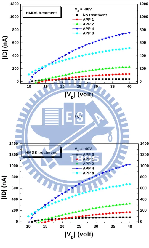
Here we focus on the influence of APPT under varied conditions which have different scanning times of APPT. They are one, two, four, eight scanning times respectively. We define that one time as APP1, two times as APP2 and so on.
As shown from Fig 3-5 to Fig 3-8, plot of drain current ID versus gate
voltage VG at various drain voltage VD and drain current ID versus gate voltage
VD at various drain voltage VG with different scanning times.
In all figures of APP0 to APP8, we can observe that APP4 has best electrical characteristic about ID-VG and ID-VD. Additionally, we plotted the comparison of
ID-VG and ID-VD in the same figure due to observe clearly, they were shown in
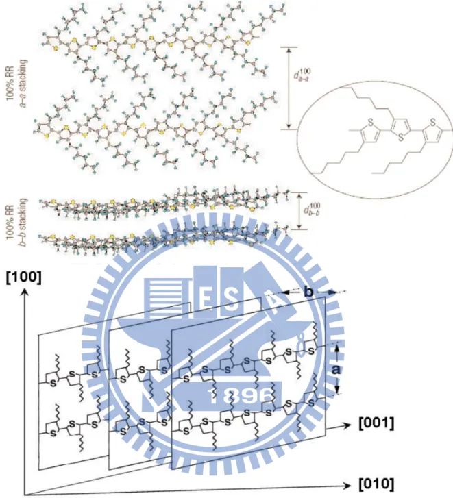
Fig 3-9. For magnitude of current at the same operating voltage, APP4 > APP8 > APP2 > APP1 > APP0. Furthermore, threshold voltage and mobility would be calculated by taking measured data into Eq.(3-1) ~ (3-3). Arrangement of threshold voltage and mobility is shown in Table 3-2(labeled as APP 0, APP 1, APP 2, APP 4, and APP 8) and Fig 3-10. The mobility in the saturation region and the threshold voltage of the OTFT are 1.9×10⁻³ cm2/Vs and -21.7V,
respectively. On the other hand, the values of field-induced current at the same gate voltage for APP4 has almost ten times higher than without treatment, as shown in Table 3-1 and Fig 3-10. After surfacing treatment, threshold voltage reduce down to -8.3V and field-effect mobility (μsat= 2.6×10⁻²cm2/Vs) which is
15-fold improvement over the mobility on bare silicon oxide.
In order to further analyze the phenomenon about surface treatment of APPT, we used atomic force microscope (AFM) to observe the surface morphology. Contact angle was measured to judgethe surface state . The contact angle and surface roughness of SiO2 with different scanning times of APPT, as
shown in Table 3-2. After surface treatment of APPT, the surface of SiO2
(contact angle < 10°) will approach hydrophobic state. With increasing times of surface treatment, contact angle will present an increasing trend. When scanning times are more than four times, the increasing trend of contact angle will be flattened gradually, as shown in Fig 3-11. In the AFM micrography, the rms values of surface roughness increases with increasing scanning times of APPT. The rms value of surface roughness changes from 6.07 nm for APP4 to 10.42 nm for APP8. The surface roughness will become more smooth after spin-coating P3HT, as shown in Table 3-2.
In general, most inorganic oxide surface including SiO2 shows hydrophilic
state while most of organic semiconductor (P3HT in this case) shows
hydrophobic states. Therefore, this mismatch has bad influence on crystalline formation of organic semiconductor fabricated on oxide substrates [47]. So it could result in good influence on increment of crystallinity and also increase field-effect mobility. After surface treatment of APPT, surface of SiO2 becomes
the improvement of field-effect mobility in our experiment. We observe the contact angle of APP4 and APP8 which are similar, but field-effect mobility of APP8 is somewhat decay compared with APP4. It is speculated that APP8 is too rough so that cause scattering effect [48].
Detailed photography of contact angle and AFM under different conditions, as shown in Fig 3-12 and Fig 3-13.
3.5.2 Spin-coating and evaporated of HMDS-treated SiO
2As mentioned in previous section, we only emphasized on surface treatment of APPT. Here, we provide another two methods of surface treatment which were spin-coating HMDS and evaporated HMDS. Many reaserchs about spin-coating HMDS could be refer to [47,49]. We will compare the difference about the three methods, and discuss the relationship of them.
As shown in Fig 3-14 and Fig 3-15, plot of drain current ID versus gate
voltage VG at various drain voltage VD and drain current ID versus gate voltage
VD at various drain voltage VG. Fig 3-14 shows the realtionship of I-V about
spin-coating HMDS, and Fig 3-15 shows the realtionship of I-V about evaporated HMDS. The same calculation for threshold voltage and mobility in saturation region is listed in Table 3-3 (labeled as APP 0, Spin-coating, Evaporation, and APP4) .
Additional measured values such as contact angle and surface roughness also are shown in Table 3-3. The two methods have obvious improvement in our experiment. The mobility in the saturation region was 4-fold for spin-coating HMDS (μsat = 7.8×10⁻³ cm2/Vs) and 11-fold for evaporated HMDS (μsat = 2.2×
10-2
cm2/Vs) higher than no treatment (μsat = 1.9×10⁻³ cm2/Vs). In Table3-3, for
important role in the interface between SiO2 and P3HT. Threshold voltage also
decreases after HMDS-treated SiO2 referred to [47]. Comparison of field-effect
mobility and threshlod voltage is shown in Fig 3-16. The plot of measured contact angle for spin-coating and evaporation is shown Fig 3-17, and Fig 3-18 shows the AFM photography. Surface of SiO2 remains smooth after spin-coating
and evaporated HMDS. Comparison of ID-VG and ID-VD is shown in Fig 3-19.
For magnitude of current at the same operated voltage, APP4 > Evaporation > Spin-coating > No treatment. So APPT is still better than the other methods of HMDS-treated SiO2 in our experiment.
3.5.3 Hysteresis
Figure 3-25 plots a typical hysteresis curve. This curve depicts the
response of the polarization, P, to the externally applied electric field, E. The
hysteresis
curve saturates at Psat when the maximum alignment of thespontaneous
polarization occurs. When the electric field is removed
instantaneously after
reaching Psat , the electronic polarization associated with the linear capacitance component decreases to zero, and the spontaneous polarization, PS, remains.Then, within milliseconds usually, the polarization decays to the remnant
polarization, Pr. For much longer times, the polarization is observed to decay
linearly with the log of time for many orders of magnitude of time [50].
The current that flows through the gate-dielectric/channel interface is widely
believed to be dominant during the operation of OTFTs. Therefore,
electronic conduction at the interface is expected directly to affect the TFT
performance. This effect is directly related to the hysteresis behavior, which
is induced by the trap sites at the interface in OTFTs.
P3HTfilms that are
deposited on the gate dielectric have many trap sites, depending on the
surface state of the gate dielectric. Undoubtedly, if the gate dielectric contains
trap sites inside the bulk, then these trapped charges may also induce
hysteresis. The hysteresis of gate dielectrics represents a potential problem
that can limit their range of applications, because this hysteresis leads to
instability of the threshold voltage in OTFTs. Various studies of hysteretic
behavior observed in OTFTs have been published [51,52]. However, in this
work, the effects of oxide trapping are assumed to be weaker than those of
interface trapping. This assumption is similar to that made in previous
investigations and is supported by changes in the extent of hysteresis with the
use of various surface modification protocols [53,54]. In recent reports, -OH
groups have been identified as the origin of the electron trapping sites that are
largely responsible for the hysteretic behavior observed in OTFTs
[55,56].Since the dielectric layer (SiO2) in this work is an -OH-rich surface, the
hysteretic
behavior is very serious (Fig.3-26). Therefore, when the surface is
transformedfrom an -OH-rich surface into a CH3-terminated surface by HMDS
surface
treatment, the hysteresis behavior decreases (Figs 3-27~3-32). Furthermore,
the formation of well-defined orientation of
P3HTgrains markedly reduces
the hysteresis by reducing the number of grain boundaries, such as when the
surface is treated by evaporation, APP 4 and APP 8 (Figs. 3-28, 3-31 and
3-27). Treatment of the surface by evaporation yields less hysteresis than the
other methods: perhaps evaporation forms the flattest surface. In one
investigation [57], the surface roughness caused strong variations in the local
field with associated scattering of carriers and the possible formation of
carrier traps. Theses results offer clear evidence that -OH groups, the
orientation of
P3HTand the surface roughness of the gate dielectric surface,
are responsible for the hysteresis behavior that is observed in OTFTs.
3.5.4 Anomalous leakage current
According to the ID-VG plots in Fig 3-33, current increases as VG
approaches 0 V, especially following surface treatment by APP. For the APP
process (Fig 3-34), the magnitude of the current as VG approaches 0 V follows
the
order APP 4 APP 8 >APP 2> APP 1, perhaps because of an anomalous
leakage current. The gate leakage current increase may have two causes –
weak
points [51], and the higher channel conductance of the OTFTs [58].
The poor
uniformity and roughness of the surfaces are the main sources of
the “weak
points, which act as local high-electric-field regions where
breakdown occurs.
These weak points enhance carrier injection and further increase the
leakage current. As presented in Fig 3-33, surface treatment by APP
increased the leakage current, because the surface became rougher. However,
although the surface of APP 8 is rougher, the leakage current is smaller than
that of APP 4.APP 4 surface treatment may enlarge the crystalline domain of
P3HT
, causing the high channel conductance. In the future, to improve the
anomalous leakage current will be studied.
3.5.5 Crystallization behavior of P
3HT
SSC-5200 differential scanning calorimeter (DSC), and the temperature was
calibrated using indium. About 5 mg of the polymer (
P3HT) sample was
weighed very accurately. It was pre-heated at 70
℃, 90
℃, 110
℃, 130
℃and 150
℃for 3 min and then cooled to room temperature at a rate of 20
℃/min. The sample was subsequently reheated to 300
℃(Run 1), cooled to
room temperature and then reheated to 300
℃(Run 2) to study its melting
behavior.
The heating rate and the cooling rate were 20 /min. All measurements were
made in a nitrogen atmosphere, and each sample was used only once to
mitigate any effect of thermal degradation after treatment at high temperature.
The thermogravimetric analysis (TGA) indicated that the thermal
degradation temperature of
P3HTwas approximately 500
℃(Fig. 3-35).
Figures 3-36~3-40 plot the melting temperature (Tm) and crystallization
enthalpy (△H) of
P3HTfor various pre-heating temperatures. These data
were collated in in Figs. 3-41 (Heat Run 1) and 3-42(Heat Run 2) and Table
3-5. The melting temperature did not vary in Run 1 or Run 2, but the enthalpy
in Run 1 increased with the pre-heating temperature up to 130
℃. The
greater enthalpy of crystallization indicated a higher degree of crystallinity -
because the higher temperature gave the molecular chain enough kinetic
energy to increase the overall crystallinity of
P3HT. However, an excessive
temperature caused the molecular chain to move too fast, reducing the
strength of its orientation. Hence, the
P3HTbaking condition herein was set to
P3HT
became amorphous after Run 1 at up to 300
℃. The crystallization
effect of
pre-heating disappeared, and the enthalpy in Run 2 was almost the samein various pre-heating temperatures.
3.5.6 XRD and UV-VIS for highly oriented crystals of P
3HT
X-ray analysis indicates that the polymer films were composed of microcrystalline domains that were embedded in an amorphous matrix, and inside these microcrystalline regions, the polymersπstack in one direction such that use the analysis with UV-VIS, because P3HT is a single bond duplet bond arranges the
conjugate structure alternately, the high polymer chain's conjugate long is longer, (Lamda max) will be bigger to the ultraviolet ray absorption wave length, moreover, the position rule higher will also have the same phenomenon UV-VIS absorption spectra revealπ-π absorption, and lamella of the interlocking side chains in the other direction [59,60]. In another investigation [61], XRD data and UV-VIS absorption spectra suggest that the molecules are oriented such that their long axis is almost normal to the film, and the π-π stacking direction is parallel to the substrate. XRD [62,63] and UV-VIS absorption [64,65] have been adopted in many studies to identify the P3HT crystal. Wang et al [66]thought that the lowest
energy (long wave length) absorbs the peak the relative strength to be higher, represents P3HT in thin film structure order, the manufacture the organic thin
film transistor original part can obtain high carries the child transport ratio, and this long wave often the absorbancy relatively strong reason lies in correlation strong relations between the P3HT member chain's, i.e. mean distance between
the P3HT chain's are few phenomenon which creates. When the P3HT is
deposited on the SiO2 surface, interchain stacking occurs in the molecular chain, so
molecular structure of P3HT exhibits high regioregularity (which is the percentage
of stereoregular head-to-tail attachments of the hexyl side chains to the 3-position of the thiophene rings),then this lamellar structure will have the edge-on orientation, its (100)-axis will be normal to the film and the (010)-axis will be in the plane of the film. Previous research has verified that good ordering is a basic requirement of improved transistor performance (better field-effect mobility) [67,68]. Figure 3-43 shows the XRD diagrams obtained following various surface treatments, including a strong and sharp diffraction peak at 5.3φ (especially after treatment with APP 4),corresponding to an intermolecular spacing of 1.636 nm in the well-organized lamellar structure, which value is consistent with the literature. The intensity of the diffraction at the same diffraction angle follows the order APP 4 > Eva >Spin > No treatment. This result was consistent with the mobility of OTFT. The surface is predicted to be more hydrophobic after APP treatment, such that the P3HT has more ordered domains along the (100)-axis and the mobility of OTFT is
therefore higher.
Figure 3-44 presents the UV-VIS absorption spectra in the region of the π-π
absorption regioregular
P3HT. The magnitude of the absorption peak at
610nm follows the order APP 4 > APP 8 > APP 2 > APP 1 > Spin > No
treatment. This result was consistent with the mobility of OTFT. The figure
indicates that modifying the surface with APP 4 increases the absorption peak
at 610 nm, revealing increases in chain extension and chain alignment.
In this chapter, XRD and UV-VIS were adopted to demonstrate that high
mobility requires an ordered structure.
(a)
(b)
Figure 3-1:
(a) The structure of APPT (b)The diagram of plasma surface(a)
(b)
TC
BC
Doping by PoCl
3Thermal oxidation
Surface treatment:
1. APPT HMDS 2. Spin-coating HMDS 3. Evaporated HMDSDeposition of P3HT by
spin- coating
Deposition of S/D contacts
through shadow mask
0 10 20 30 40 40 60 80 100 120 140 160 180 200 40 60 80 100 120 140 160 180 200 |I D | (n A) |VG| (volt) VD = -20V VD = -30V VD = -40V VD = -50V APP HMDS 1 (a) 10 15 20 25 30 35 40 0 100 200 300 400 500 0 100 200 300 400 500 |I D | (nA) |VD| (volt) VG = 0V VG = -10V VG = -20V VG = -30V VG = -40V VG = -50V APP HMDS 1 (b)
Figure 3-5:
Surface treatment of APPT HMDS 1 for OTFT0 10 20 30 40 50 100 150 200 250 300 350 400 450 500 50 100 150 200 250 300 350 400 450 500 |I D | (n A) |VG| (volt) VD = -20V VD = -30V VD = -40V VD = -50V APP HMDS 2 (a) 10 15 20 25 30 35 40 0 100 200 300 400 500 600 700 0 100 200 300 400 500 600 700 |I D | (nA) |VD| (volt) VG = 0V V G = -10V VG = -20V VG = -30V V G = -40V VG = -50V APP HMDS 2 (b)
Figure 3-6:
Surface treatment of APPT HMDS 2 for OTFT0 10 20 30 40 200 400 600 800 1000 1200 200 400 600 800 1000 1200 |I D | (nA) |VG| (volt) VD = -20V V D = -30V VD = -40V VD = -50V APP HMDS 4 (a) 10 15 20 25 30 35 40 0 200 400 600 800 1000 1200 1400 1600 1800 2000 0 200 400 600 800 1000 1200 1400 1600 1800 2000 |I D | (nA) |VD| (volt) VG = 0V VG = -10V VG = -20V V G = -30V VG = -40V VG = -50V APP HMDS 4 (b)

![Table 2-1: Field-effect mobility and ON/OFF ratio of samples prepared from different solvents and process condition [14]](https://thumb-ap.123doks.com/thumbv2/9libinfo/8243098.171404/30.892.129.842.133.835/table-mobility-samples-prepared-different-solvents-process-condition.webp)