國 立 交 通 大 學
電子工程學系 電子研究所碩士班
碩 士 論 文
閘極介電層氧化釓於
硫鈍化後砷化鎵基板之電物性研究
The Electrical and Material Characteristics
of Gd
2O
3Gate Dielectric on Sulfided GaAs Substrate
研 究 生:曾 治 國
指導教授:簡 昭 欣 博士
國 立 交 通 大 學
電子工程學系 電子研究所碩士班
碩 士 論 文
閘極介電層氧化釓於
硫鈍化後砷化鎵基板之電物性研究
The Electrical and Material Characteristics
of Gd
2O
3Gate Dielectric on Sulfided GaAs Substrate
研 究 生:曾 治 國
指導教授:簡 昭 欣 博士
閘極介電層氧化釓於硫鈍化後
砷化鎵基板之電物性研究
The Electrical and Material Characteristics
of Gd
2O
3Gate Dielectric on Sulfided GaAs Substrate
研 究 生:曾 治 國
Student:Chih-Kuo Tseng
指導教授:簡 昭 欣 博士 Advisor:Dr.
Chao-Hsin Chien國 立 交 通 大 學
電子工程學系 電子研究所碩士班
碩 士 論 文
A Thesis
Submitted to Department of Electronics Engineering & Institute of Electronics College of Electrical Engineering and Computer Science
National Chiao Tung University in partial Fulfillment of the Requirements
for the Degree of Master
in
Electronics Engineering June 2007
Hsinchu, Taiwan, Republic of China
中華民國九十六年六月
I
閘極介電層氧化釓於硫鈍化後
砷化鎵基板之電物性研究
研 究 生:曾 治 國 指 導 教 授:簡 昭 欣 博士
國立交通大學
電子工程學系 電子研究所碩士班
摘 要
本論文中, 將選擇跟砷化鎵基板有較穩定特性的稀土族元素釓之氧化 物作為閘極介電材料,接著我們利用表面預備製以及後熱退火來探討氧化 釓與其砷化鎵之介面的電物性研究。 首先,對於砷化鎵基板的濕式化學清潔,發現鹽酸溶液對於表面會呈 現砷化物居多的情形,接著做氨水蝕刻溶液去除多餘的砷化物。當清潔步 驟完成時,接著馬上進行硫鈍化砷化鎵表面的工作。在介電質沉積之前, 硫鈍化的目的可以降低時表面產生的大量介面缺陷氧化層,缺陷氧化層就 會使得往後的電物性結果受到極大的影響。我們發現硫化物同時和砷或鎵 形成反應,而硫化鎵鍵結比硫化砷鍵結更容易隨著硫化處理的溫度增加而 讓鍵結穩定,那是因為堅強的鍵結情形,這樣的話就能降低氧化釓與其砷 化鎵電容結構的表面自然氧化層以及介面捕捉狀態密度。II 我們也發現硫化銨與水溶液或醇類溶液結合可以有效解決金屬與砷化 鎵的費米能階釘札情形。混合的硫化銨和丁醇(butanol)是最有效率可以降低 蕭基特能位障的溶液,這是因為硫鈍化可以去除大量的介面氧化層。 另外,後退火幫助氧化釓與砷化鎵接面的品質得到改善;改變不同退 火環境可以得到在電容-電壓以及電流-電壓不同的特性。在 500-600 度的含 氧氣體下呈現較少色散的電容-電壓曲線和低的漏電流程度,反之惰性的氬 氣或氮氣含量氣體則得到相反結果。另一方面,吸水造成的衰退情形對我 們已沉積的高介電質氧化釓並沒有太大明顯,透過韋伯(Weibull)分佈研究 下,氧化釓在砷化鎵上的電容即使一個月時間依然可以得到相同的電特 性。因此,我們推斷高穩定的氧化釓與其砷化鎵介面可以整合硫鈍化預先 處理和介電質退火過程去實現金屬-氧化物-半導體結構的高速元件應用。
III
The Electrical and Material Characteristics of
Gd
2O
3Gate Dielectric on Sulfidized GaAs Substrate
Student: Chih-Kuo Tseng Advisor: Dr. Chao-Hsin Chien
Department of Electronics Engineering and Institute of Electronics National Chiao Tung University, Hsunchu, Taiwan
ABSTRACT
In this thesis, the rare-earth oxide of Gd2O3 was used as high-k gate
dielectric material, which is highly stabilized with GaAs, and we studied the material and electrical properties of the Gd2O3/GaAs structures through surface preparation procedures and post thermal annealing, respectively.
At first, for the wet chemical cleaning, it was found that the GaAs surface preferred to form arsenic chemical species after etching in HCl solution, and
subsequent NH4OH solution assisted to remove these excess arsenic-related
defects. After that, we performed various kinds of the sulfur-based pretreatment to passivate the cleaned GaAs substrate. The purpose of formed sulfur–terminated GaAs surface is to restrain the growth of defective oxide layers prior to and during the dielectric deposition; since they indeed cause the degradation of the following electrical characteristics. We found that sulfur atoms can react with both arsenic and gallium elements; an increase in sulfidized temperature intends to form the Ga-S rather than As-S chemical bonding
IV
because of the stronger bonding strength, which in turn facilitating to decrease surface native oxides and interface trap density in Gd2O3/GaAs capacitors.
We also observed that (NH4)2S aqua or combining with alcohol-based
solution can alleviate the well-known Fermi level pinning on metal/GaAs interface. The mixed solution of the (NH4)2S and the butanol was found to be effectively decrease the Schottky barrier height due to the removal of substantial interfacial oxides as well as the definite sulfide passivation.
In addition, the post-deposition annealing further boosted the quality of Gd2O3 thin film with improved Gd2O3/GaAs interface; moreover, changing the annealing atmosphere showed several characteristic differences in C-V and I-V curves. The O2-contained gas at 500-600
o
C revealed the smaller C-V frequency dispersion and lower leakage current level, whereas the inert Ar or N2-contained gas revealed the opposed results. On the other hand, the humidity induced
degradation is not obvious for deposited Gd2O3 high-k dielectric that the
identical electrical properties can be preserved in Gd2O3/GaAs capacitors up to one month through investigation of the Weibull distribution. Therefore, we
conclude that the highly stable Gd2O3/GaAs interface can be achieved
integrating the sulfide pretreatment and dielectric annealing processes, which can be considered as the potential structure for metal-oxide-semiconductor device application.
V
致 謝
在短短兩年的碩士班研究生涯,首先感謝指導教授 簡昭欣 博士給予 實驗室學生豐富專業知識的指導,以及老師為人處事更是我們應當學習的 目標,另外老師對學生的用心及精神更是讓大家感動不已。其次感謝國家 奈米實驗室裡的楊明瑞學長,不管在實驗或討論問題上提供了相當大的幫 忙,才得以完成學生的碩士論文。 特別感謝鄭兆欽學長,給予我們極大的鼓勵和幫忙,從學長的做實驗 細心態度下學習很多做事情的精神和經驗,相信可以對自己以後有幫助, 也祝他在未來人生能一切順利平安。另外,包括楊紹明學長、陳世璋學長 以及沈志彥學長,感謝他們不僅解答實驗上的疑問,在日常生活中亦不斷 地鼓勵我上進。也謝謝實驗室的其他同學:家豪、熊哥、石頭、小劉、阿壘、 阿心和學弟們:弘森、欣哲、Rain、宣凱、敬倫、宇彥、猛飛,陪我一同走 過兩年的碩士生活,以及陪我在籃球場上奔跑的日子,謝謝實驗室的大家 給我留下許多快樂的回憶。 最後,我要由衷感激親愛的父母,感謝您們辛苦的栽培及默默付出, 用心奉獻整個家庭,使得孩子們得以全心投入學業;謝謝優秀的兩位哥哥 和老弟的加油與打氣,也因為你們讓爸媽得以減輕辛勞;感謝可愛的女友 雅蓮,給了我全力的支持與鼓勵。VI
Contents
Abstract (Chinese) --- Ⅰ Abstract (English) --- Ⅲ Acknowledgement --- Ⅴ Contents --- Ⅵ Figure Captions --- ⅨChapter 1 Introduction
1-1 General Background --- 1 1-2 Motivation --- 3 1-3 Organization --- 4Chapter 2 The Cleaning Process of Gallium Arsenide Substrate
2-1 Introduction --- 72-2 Experimental Procedure --- 10
2-3 Results and Discussion --- 11
2-3-1 XPS of cleaning GaAs substrate --- 11
2-3-2 Surface morphology of cleaning GaAs substrate --- 14
VII
Chapter 3 The Sulfur Passivation on Gallium Arsenide Substrate
3-1 Introduction --- 27
3-2 Experimental Procedure --- 29
3-3 Results and Discussion --- 31
3-3-1 XPS and PL of the sulfided GaAs substrate --- 31
3-3-2 surface roughness of the sulfided GaAs --- 35
3-3-3 electrical characterization of the sulfided GaAs --- 36
3-4 Summary --- 37
Chapter 4 Electron-beam evaporated Gd
2O
3Gate Dielectric On
GaAs Substrate
4-1 Introduction --- 554-2 Experimental Procedure --- 56
4-3 Electrical and Material Characteristics --- 57
4-3-1 C-V and I-V characteristics of Pt/ Gd2O3/ GaAs structure --- 57
4-3-2 xps characteristic of Gd2O3 film on GaAs substrate --- 63
4-3-3 surface morphology of Gd2O3 film on GaAs substrate --- 65
VIII
Chapter 5 Conclusions and Suggestions for Future Work
5-1 Conclusions --- 93
5-2 Future Work --- 94
References --- 96
IX
Figure Captions
Chapter 1 Introduction
Fig.1-2 Advantage of GaAs substrate compared to general Si material. Fig.1-2 Predicted band offsets on GaAs with different high-k materials.
Chapter 2 The Cleaning Process of Gallium Arsenide Substrate
Fig. 2-1(a) As 2p and (b) As 3d core-level spectra with different diluted HCl concentration. Fig. 2-2(a) Ga 2p and (b) Ga 3d core-level spectra after different diluted HCl concentration. Fig. 2-3(a) As 2p and (b) Ga 2p core-level spectra after different diluted HCl concentration
and cleaned cycles.
Fig. 2-4 The fitting result of (a) As 2p and (b) Ga 2p core-level spectra after diluted HCl concentration.
Fig. 2-5 The fitting results of As 2p core-level spectra with diluted HCl solution following by different NH4OH solutions.
Fig. 2-6 The arsenic compound ratio with diluted HCl solution following by different NH4OH
solutions.
Fig. 2-7 AFM image of cleaned GaAs substrate with different clean methods: (a) HCl (b) HCl+NH4OH (c) NH4OH.
Fig. 2-8 Surface roughness of cleaned GaAs substrate with different clean methods: (a) HCl (b) HCl+NH4OH (c) NH4OH.
X
Table 2-1 The fitting results of the GaAs component from photoelectron spectra
Table 2-2 The fitting results of the GaAs component from photoelectron As 2p spectum. Table 2-3 The fitting results of the GaAs component from photoelectron Ga 2p spectum Table 2-4 The ratio of GaAs component with diluted HCl solution following by different
NH4OH solutions.
Chapter 3
The Sulfur Passivation on Gallium Arsenide SubstrateFig. 3-1 (a) As 2p and (b) Ga 2p core-level spectra after different sulfide methods.
Fig. 3-2 (a) S 2p spectra by three sulfur passivation before subtraction and (b) after subtraction Ga 2s peak from S 2p peak.
Fig. 3-3 (a) As 2p and (b) Ga 2p core-level spectra of the sulfided samples against moisture with spectra after 1week .
Fig. 3-4 Photoluminance of Gd2O3/ GaAs sulfided by (NH4)2S solution with different (a)
temperature and (b) concentration.
Fig. 3-5 Photoluminance of Gd2O3/ GaAs sulfided by Na2S solution with different (a)
temperature and (b) concentration.
Fig. 3-6 (a) As 2p (b) Ga 2p core-level spectra of sulfided GaAs at various treatment temperature: (i) without sulfide (ii) sulfide at room temperature (iii) sulfide at 50oC (iv) sulfide at 80oC.
XI
Fig. 3-8 (a) As 2p and (b) As 3d spectra of GaAs after two sulfur concentration:
(i) cleaned (ii) sulfide at 0.5% concentration (iii) sulfide at 2% concentration. Fig. 3-9 (a) Ga 2p and (b) Ga 3d spectra of GaAs after two sulfur concentration:
(i) cleaned (ii) sulfide at 0.5% concentration (iii) sulfide at 2% concentration. Fig.3-10 (a) As 2p and (b) Ga 2p core level spectra after HCl+NH4OH solution with two
sulfided temperature.
Fig. 3-11 GaAs component ratio of the HCl、NH4OH solutions cleaned with two sulfide
temperature.
Fig. 3-12 Surface morphology of HCl cleaned GaAs substrate after different sulfide condition: (a) without sulfidation (b) 1%, RT (c) 1%, 80oC.
Fig. 3-13 Surface morphology of HCl +NH4OH cleaned GaAs substrate after different sulfide
condition: (a) without sulfidation (b) 1%, 80oC.
Fig. 3-14 Surface morphology of NH4OH cleaned GaAs substrate after different sulfide
condition: (a) without sulfidation (b) 1%, 80oC.
Fig. 3-15 Surface roughness of cleaned GaAs with different sulfidation
Fig. 3-16 I-V curves of Al metal contact to n-GaAs substrate with different surface treatment. Fig. 3-17 Extraction of Schottky barrier height(SBH) with Al metal on n-type GaAs
Fig. 3-18 Schottky diode parameters with (NH4)2S solution after (i) no-anneal (ii) 400oC N2
anneal (iii) 500oC N2 anneal.
XII C3H7OH (iii) C4H9OH.
Fig. 3-20 Schottky barrier height(SBH) with sulfur solution and different solvents: (i) H2O (ii)
C3H7OH (iii) C4H9OH.
Fig. 3-21 I-V curves of Schottky diode (a) with and (b) without sulfide.
Chapter 4
Electron-beam evaporated Gd2O3 Gate Dielectric On GaAs SubstrateFig. 4-1 (a)-(d) Multi-frequency C-V characteristics of Pt/Gd2O3/GaAs MOS capacitor with
different surface treatment.
Fig. 4-2 (a)-(d) The hysteresis of 10kHz frequency of Pt/Gd2O3/GaAs MOS capacitor with
different surface treatment.
Fig. 4-3 (a) Multi-frequency C-V curve with HCl+NH4OH +Sulfide treatment (b) The C-V
dispersion with different surface treatments for Pt/Gd2O3/GaAs MOS capacitors.
Fig. 4-4 (a) The 10kHz frequency C-V and (b)hysteresis characteristics of Pt/Gd2O3/GaAs
MOS capacitor with different clean and sulfide method.
Fig. 4-5 (a) The I-V curve characteristics and (b) Jg(@V=+1v) of Pt/Gd2O3/GaAs MOS
capacitor with different clean and sulfide method.
Fig. 4-6 Density of state on Gd2O3/GaAs interface with different clean and sulfide method.
Fig. 4-7 (a)-(d) Multi-frequency C-V and hysteresis using 10k Hz frequency characteristics of Pt/Gd2O3/GaAs MOS capacitor with two cleaning method: (i) HCl+NH4OH (ii)
XIII NH4OH
Fig. 4-8 (a) Multi-frequency C-V (b) the hysteresis using 10k Hz frequency and (c) density of state characteristics of Pt/Gd2O3/GaAs MOS capacitor with two cleaning method: (i)
HCl+NH4OH (ii) NH4OH
Fig. 4-9 (a) The I-V curve characteristics and (b) Jg(@V=+1v) of Pt/Gd2O3/GaAs MOS
capacitor with different clean methods and sulfide methods.
Fig. 4-10 (a)-(c) Multi-frequency C-V frequency characteristics of Pt/Gd2O3/GaAs MOS
capacitor with three cleaning methods: (i) HCl (ii) HCl+NH4OH (iii) NH4OH
Fig. 4-11 (a)-(c) The C-V characteristics and Dit of Pt/Gd2O3/GaAs MOS capacitor with three
cleaning methods: (i) HCl (ii) HCl+NH4OH (iii) NH4OH under optimum
sulfidation.
Fig. 4-12 (a)-(b) The leakage current characteristics and Jg v.s CET of Pt/Gd2O3/GaAs MOS
capacitor with three cleaning methods: (i) HCl (ii) HCl+NH4OH (iii) NH4OH under
optimum sulfidation.
Fig. 4-13 The Weibull distribution of Pt/Gd2O3/GaAs MOS capacitor with three cleaning
methods: (i) HCl (ii) HCl+NH4OH (iii) NH4OH after 1 week.
Fig. 4-14 The TEM pictureof Pt/Gd2O3/GaAs MOS capacitor with NH4OH under optimum
sulfidation.
Fig. 4-15 The EDS distribution signalof Pt/Gd2O3/GaAs MOS capacitor with NH4OH under
XIV
Fig. 4-16 (a)-(e) Multi-frequency C-V frequency characteristics of Pt/Gd2O3/GaAs MOS
capacitor with different gas ambient : (i) O2 500oC (ii) Ar500oC (iii) N2500oC (iv)
Ar / O2 500oC (v) Ar / O2 600oC
Fig. 4-17 (a)-(e) The hysteresis width of Pt/Gd2O3/GaAs MOS capacitor with different gas
ambient : (i) O2 500oC (ii) Ar500oC (iii) N2500oC (iv) Ar / O2 500oC (v) Ar / O2
600oC
Fig. 4-18 (a) The 10k Hz frequency and (b) hysteresis trend of Pt/Gd2O3/GaAs MOS
capacitor with different gas ambient : (i) O2 500oC (ii) Ar500oC (iii) N2 500oC (iv)
Ar / O2 500oC (v) Ar / O2 600oC
Fig. 4-19 (a) The dispersion and (b) leakage distribution characteristics of Pt/Gd2O3/GaAs
MOS capacitor with different gas ambient : (i) O2 500oC (ii) Ar 500oC (iii)
N2500oC (iv) Ar / O2 500oC (v) Ar / O2 600oC
Fig. 4-20 XPS spectra of the annealed Gd2O3 film at 500°C for 10 s. (a) the As 3d core level;
(b) the Ga 3d core level.
Fig. 4-21 XPS spectra of the annealed Gd2O3 film at 500°C for 10 s. (a) the Gd 3d core level;
(b) the Gd 4d core level.
Fig. 4-22 XPS spectra of the annealed Gd2O3 film at 500°C for 10 s. (a) the As 3d and Ga 3d
core level; (b) the O 1s core level.
XV treatment.
Fig. 4-24 XRD spectra of (i) n-GaAs(100) and (ii) 500oC annealed Gd2O3/ n-GaAs(100)
Fig. 4-25 Surface roughness of Gd2O3 on GaAs substrate after Ar/O2 (500oC 10s) anneal with
different surface treatments.
Fig. 4-26 Surface roughness of Gd2O3 on GaAs substrate after Ar/O2 (500oC 10s) anneal with
1
Chapter 1
Introduction
1-1 General Background
Advancements in the performance of CMOS devices employing silicon substrates have been consistently achieved by shrinking critical MOSFET dimensions. Whiles critical dimensions keep decreasing to meet the demand for smaller and faster chips, the associated challenges will become increasingly difficult to address. As theoretical limits are reduced in the silicon CMOS world, referenced to MOSFETs based on compound semiconductor substrates have appeared in the International Technology Roadmap for Semiconductor [2] .Nanoscale device technology is driving intense study of thin dielectric layers on semiconductors. The aggressive scaling of Si CMOS technology calls for identifying high k dielectrics to replace SiO2 and oxynitride in gate related applications [3]. About the substrate, Si and GaAs will be compared in the Fig. 1-1. The fundamental material requirements for the alternative gate dielectric are
very challenging in order to achieve performance comparable to SiO2. These
requirements include dielectric constant, band gap, conduction band offset, high recrystallization temperature (for amorphous dielectrics only), low oxygen
2
diffusivity, The rare earth dielectric oxides have a high conduction band offset over 1 eV and show good thermodynamic stability in contact with GaAs, hence are considered as a very attractive candidate among several binary metal oxides currently in contention[4] .The GaAs metal-oxide-semiconductor field-effect transistor (MOSFET) in the driven by their applications in the high-speed circuit, which a low-leakage current ,and high-electrical strength[5]. Fig. 1-2 illustrate the energy band offset about GaAs substrate [6], and the difference of
conduction band between GaAs and Gd2O3 is 1.8e V, which can reduce the
3
1-2 Motivation-Development of Gate Dielectric of GaAs
Substrate.
Over the last few decades, there has been a dramatic increase in the number of publications on gate oxide with GaAs. For instance, in 1963 Revesz first appear that who use “anodic oxide” method to growth oxide, but the film morphology was too coarse [7]. In 1965, Becke, Hall and White used hot oxidation to growth SiO2 as gate oxide [8]. Hasegawa et al. have introduced the SiO2 or Si3N4 ultrathin film as an interfacial control layer between a GaAs and a gate dielectric [9].Wada have proposed an atomic layer passivation method using atomically thin compound layer [10]. Of the proposed alternative gate dielectrics for the GaAs, an epitaxially grown Gd2O3 film stands out as a stable insulating layer for the MOSFETs due to a lowest interface-state density below 1010 cm−2 eV−1 for both the inversion channel and the depletion-mode GaAs
MOSFETs[11]、[12]. Therefore, the Gd2O3 on GaAs is the better surface
passivation required for the efficient protection of GaAs from the air exposure and the deposition-induced degradation.
4
1-3 Organization of the Thesis
In Chapter 2, we developed the cleaning process of GaAs substrate. Different diluted etching solutions were treated for GaAs wafer cleaning. Various material analysis techniques, such as Atomic Force Microscopy (AFM) and X-ray Photoelectron Spectroscopy (XPS) were performed to observe the surface morphology and surface binding behavior of GaAs substrate after the cleaning procedure.
In Chapter 3, with the optimized cleaning procedure of GaAs wafer, the surface passivation was needed. The chemical wet solution was prepared to treat the GaAs surface in order to reduce the growth of native AsOx and GaOx oxide when exposed to air ambient. Various material analysis techniques, such as Atomic Force Microscopy (AFM), X-ray Photoelectron Spectroscopy (XPS) and Photoluminescence (PL), were performed to observe the surface morphology, surface binding behavior of GaAs substrate and surface trap after the cleaning and passivation procedure. Electrical analysis was discussed with Schottky barrier height reduction according to aluminum contact with n-type GaAs.
In Chapter 4, the thesis research focus on this chapter, the metal-insulator-semiconductor structure was fabricated, the optimized surface
5
treatment, post deposition anneal and e-beam evaporated Gd2O3 high-k films were included. Various material analysis techniques, such as Atomic Force Microscopy (AFM), X-ray Photoelectron Spectroscopy (XPS) were performed to observe the films morphology and surface binding behavior of GaAs substrate after the film deposition procedure and metal-insulator-semiconductor structure cross section behavior. Electrical analysis such as C-V and I-V characteristics were used to discuss the capacitor properties.
Finally, in Chapter 5 gave the conclusion and suggestions of this thesis for the future work.
6
Fig.1-1 Advantage of GaAs substrate compared to general Si material.
Properties@300K Si GaAs
Mobility (cm 2 /V.s)
electrons 1450 8000
holes 500 400
Energy gap (eV) 1.12 1.43
Intrinsic resistivity (Ω-cm)
7
8
Chapter 2
The Cleaning Process of Gallium Arsenide Substrate
2-1
Introduction
The last two decades have seen growing importance places on research in
Gallium Arsenide surface clean. Surface clean is the most important process in
order to improve the device performance. Gallium Arsenide is easy to oxidize
during the short time, and the native oxides description change with the acid or
alkaline solution. In order to achieve the high-quality surface properties, the
following conditions are: (1) metal and particle-free surface (2) the thin surface
native oxide (3) flat surface morphology. For example of the mainstream silicon
devices, surface terminated by silicon hydride are gaining popularity for the
growth of gate oxide, which is used in the fabrication of deep submicron
ultra-large integrated circuits. Accordingly, several different methods for GaAs
surface cleaning have been reported. In the earlier stage, heating cleaning at high
9
above 200oC will is mainly gallium oxide whereas it is an arsenic-rich mixture
of As and Ga oxides after the standard procedure [13]. The desorption
temperature: (1) AsOx: around 200 oC; (2) As element: around 350 oC; (3) GaOx:
around 500 oC [14]. Since volatile or unstable oxides are removed during the
temperature ramp, it is only a Ga2O3-like oxide that remains on the surface
above 500 oC. Menda et al provide an excellent review of the method and
findings issues related to wet cleaning use [15]. In the thermal treatments at
temperature higher than 570 oC, thermal facets are introduced on GaAs surface.
It reported that the native oxide on the GaAs surface dipped in a HF solution can
be removed in vacuum at 490 oC and this is arsenic-rich from their analysis.
Alternative method of reduction of the density of protrusions on a cleaned GaAs
surface by arsenic-free high-temperature surface cleaning was found decrease
the temperature ramp-up rate of the thermal cleaning. Two-step-heating
sequence in arsenic-free high-temperature surface method for two-dimensional
10
one-step heating [16]. The following is an instance of ion-cleaning, an undoped
substrate after conventional thermal cleaning under an As4 flux is smoother than
that of a Si-doped substrate. The surface roughness of Si-doped was greatly
improved by cleaning using hydrogen radicals(H‧) at temperature of about 400
o
C, the results indicate that the (H‧) treatment of non-smooth substrate is useful
for obtaining smooth and clean surface[17]-[18]. However, the above-mentioned
cleanings were thermal heating method. The wet chemical cleaning results of
this study could have considerable impact on passivation of surface behavior.
The effective wet chemical cleaning process used NH4OH mixture to remove
particles and metals as a first step of wet-chemical cleaning and acidic peroxide
mixture to remove residual metallic contaminants and control the components of
oxide layer as a second step of wet-chemical cleaning [20]. Surface modification
of GaAs during argon ionic cleaning and nitridation has reported [21]. During
argon ionic bombardment, the values of FWHM of Ga3d peak and energy gap
11
gas can due to a new contribution of Ga-N bonds in the XPS spectra. After
cleaning with HCl or H3PO4, elemental As remained on GaAs surface , but
elemental As is easily remove by NH4OH cleaning [22].Unlike the silicon
substrate was only one elemental in comparison to the binary of GaAs substrate.
The study searched some wet chemical treatments, which were tested in our
fabrication process, and sought for the optimized cleaning procedure for GaAs
substrate.
2-2 Experimental Procedure
The experimental wafers were the n-type (Si doped) 2-inch GaAs(100), and
the doped concentration is about 1018 cm-3. Wet-cleaning method was the
feasible cleaning method for the experiments. The samples were washed with
deionized water (D.I.W) for 3min to remove the larger particles. In this work,
we propose the following two procedure cleaning method. First, the HCl acid
12
solution remove the native oxide, these wafers were washed with deionized
water (D.I.W) for 3min to bear the residual oxide and Ca-Cl bond. And the
NH4OH alkali solution was used as cleaning and broad-spectrum way. After the
solution, wafers were washed with deionized water (D.I.W) for 3min to remove
cation. Eventually, all samples were dry with N2 blowing, and the surface
morphology was characterized immediately by atomic force Microscopy(AFM);
surface chemistry was measure by X-ray Photoelectron spectroscopy ( XPS).
2-3 Results and Discussion
2-3-1 XPS of cleaning GaAs substrate
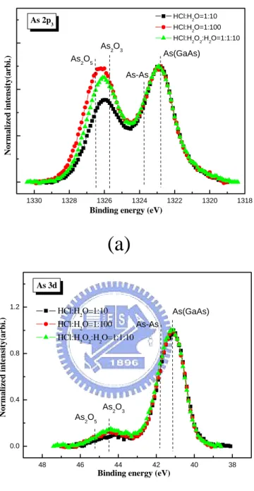
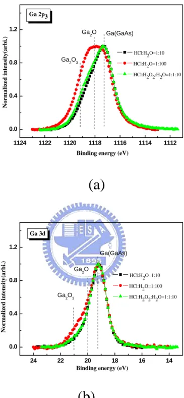
In this study, by the use of X-ray photoelectron spectroscopy, the GaAs surface oxides accurately measure the binding energies associated with the 2p and 3d in the X-ray photoemission spectra. The X-ray photoelectron experiment was performed at the National Device Laboratory (NDL) in Hsinchu, Taiwan. The excitation was accomplished using a monochromatic Al Kαration source(h ν=1486.6eV ). Fig. 2-1 shows the As 2p peak and As 3d peak spectra with different HCl solution [22]. In Fig.2-1(a) spectra, the substrate peak As(GaAs)
13
binding energy is assigned as 1322.7 ± 0.05eV; As-As metal peak signal is assigned as 1323.7 ± 0.05eV, which is spacing to As(GaAs) signal with 1eV and results from following equation:
) ( 2 3 4 3 + → 4 + + 2 ↑ + + − − H As GaCl Cl H GaAs o (1)
And then, 1325.7 ± 0.05eV for As2O3; 1326.5 ± 0.05eV for As2O5 [23]-[28], and the clean method of HCl/D.I.W.(10%) can reduce the arsenic oxide of GaAs compared to the method of HCl/D.I.W.(10%) or added H2O2 solution to diluted HCl solution. In Fig.2-1(b) spectra, the As 3d spectra also can see the oxide signal at high binding energies, the substrate peak As(GaAs) binding energy is assigned as 41.1 ± 0.05eV; As-As metal peak signal is assigned as 41.7 ± 0.05eV which spacing is similar to As 2p with 1eV; 44.5 ± 0.05eV for As2O3; 45
± 0.05eV for As2O5. Two orbit spectra both can see the cleaning surface
chemistry after HCl solution. Fig.2-2 is the Ga orbit spectra, and in Fig. 2-2(a) the GaAs substrate of Ga 3d spectra is assigned at Ga(GaAs):1117 ± 0.05eV;As opposed to arsenic metal, gallium metal was not easily to form; 1118 ± 0.05 for
Ga2O; 1119 ± 0.05eV for Ga2O3.The method of HCl/D.I.W.(1%) received the
14
indicate the same message, the gallium oxide peak is less than the method of HCl/D.I.W.(10%) solution. And the assigned peaks are described as follows:
19.2 ± 0.05eV for Ga(GaAs); 19.9 ± 0.05eV for Ga2O ;21.05 ± 0.05eV for
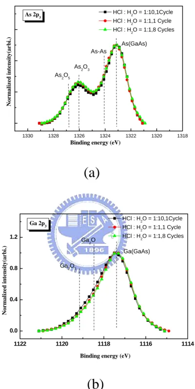
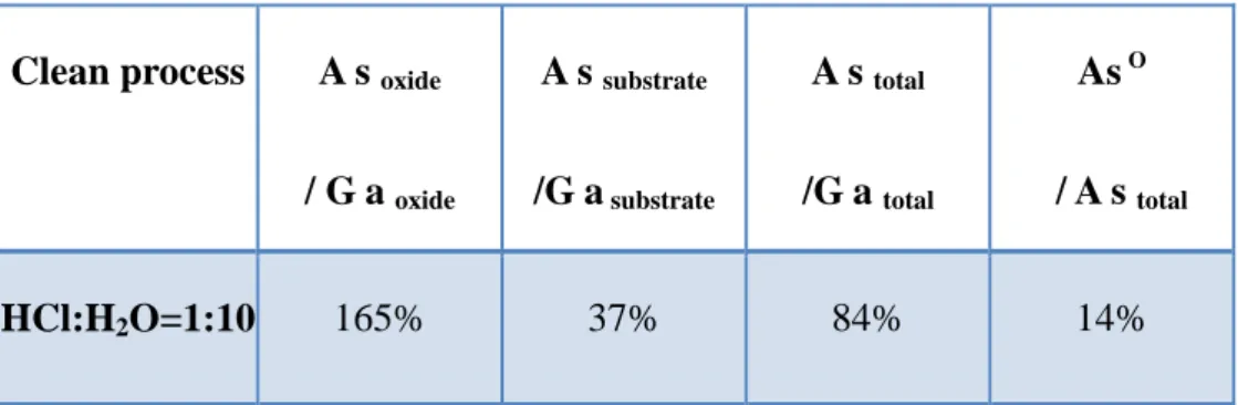
Ga2O3.To go a step further, finding the optimum concentration and cleaning cycle are described as follows. Fig. 2-3 shows the As 2p peak and Ga2p peak spectra with different HCl solution cycles. The concentration of 10% (HCl/D.I.W.) and 1% both had advantage of different orbit spectra. In the Fig.2-3(a) is the As 2p peak spectra, the concentration of 10% has resulted in As2O3 (~1326eV) component slightly less than another. On the contract, the concentration of 1% has caused Ga-O less than 10% solution shown in Fig.2-3(b). The fitting results of photoelectron spectra are shown in Fig. 2-4, and Table 2-1 is the ratio of component. Because of sensitivity (photo-ionization cross sections) to different elements, the ratio of arsenic to gallium is needed divide by 1.27(As2p3=27.2 / Ga2p3=21.4). After HCl solution with concentration of 10%, the GaAs surface is arsenic oxide-rich and the ratio percentage is 165%. It also remains As elemental, the percentage of As element over total arsenic signal was 14%. The As element easily reacted with oxygen compared to Ga elemental, and the arsenic oxides were unstable during thermal process [29]. Table 2-2 and Table 2-3 are the fitting results of the GaAs
15
component from photoelectron As 2p and Ga 2p spectra. The Equation (2) is the arsenic oxides reaction equilibrium equation. The arsenic oxide desorbs at around 200oC, and the other for As element at around 350 oC. On the contrast,
Ga oxide (Ga2O) starts to desorb at around 500
o
C, and the volatile Ga2O is result from Eq.(3). The Ga2O3 remains on the surface above 500
o
C, and it has advantage of thermal stability [14].
2 3 2 2 3 2 2( 4 )
As O + GaAs→Ga O + As orAs ↑ (2)
2 3
4
3
22
2(
4)
Ga O
+
GaAs
→
Ga O
↑ +
As orAs
↑
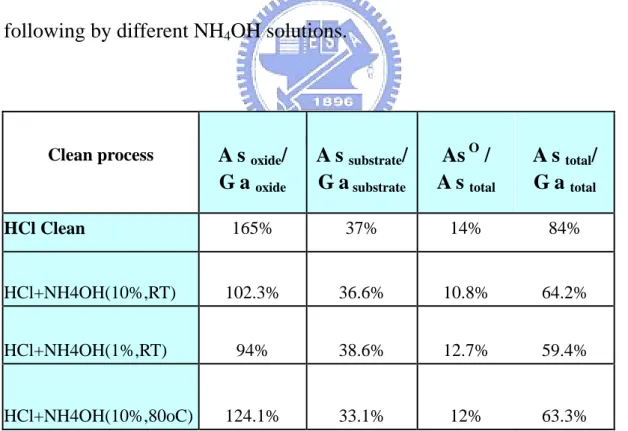
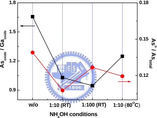
(3)Fig. 2-5 and Table 2-4 illustrate improvement experiments, by adding NH4OH solution after HCl solution cleaning [22]、[30]. Three ammonia conditions were
NH4OH/D.I.W.(1%,RT) 、 NH4OH/D.I.W.(10%,RT) and NH4OH/D.I.W.
(10%,80oC), respectively. The As element over total arsenic signal ratio really is
reduced because of As elemental is dissolved in NH4OH solution, and arsenic
oxide over gallium oxide ratio also had decreased. The better conditions of ammonia solution are 1% and 10% at room temperature. Fig. 2-6 shows the
arsenic compound ratio with different NH4OH method, and the fewer As
16
respectively.
2-3-2 Surface morphology of cleaning GaAs substrate
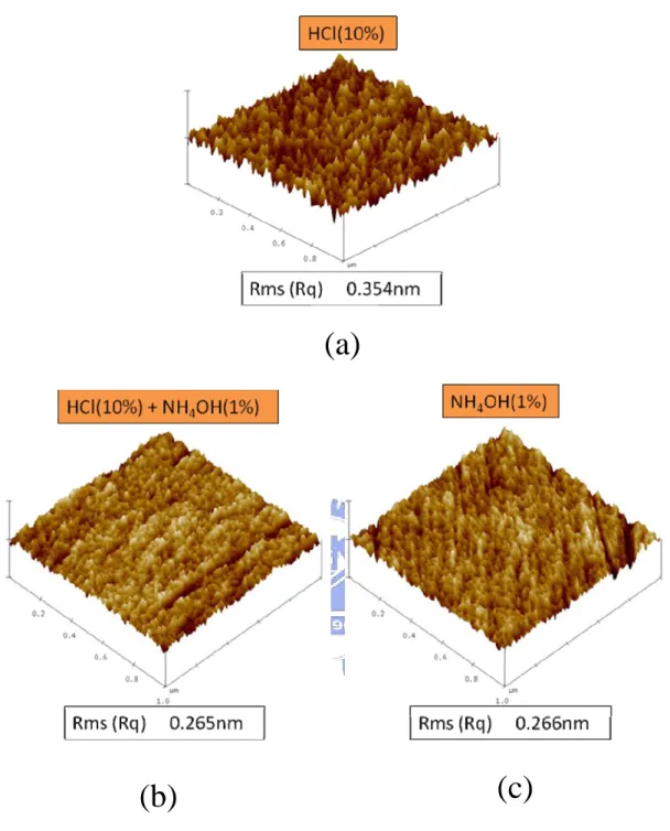
Fig. 2-7(a) shows the surface of n-type GaAs substrate after cleaning of diluted HCl / D.I.W. etching solution with concentration of 10%. After HCl solution cleaning, the wafer was washed by D.I.W. for three minutes because the Ga-Cl bond is highly soluble in the water [22].The As element appearance had discuss in chapter 1. Fig. 2-7 (b) shows the surface roughness of n-type GaAs
substrate after cleaning of diluted HCl/D.I.W.(10%) and NH4OH/D.I.W.(1%) ,
and D.I.W. was used after each step cleaning. It is known that the NH4OH
cleaning leads to the obvious decrease of As elemental component, and the
surface roughness of NH4OH-cleaned GaAs was flatter. The surface roughness
also slightly results from As element. In the Fig. 2-7(c), only one etching
solution of NH4OH/ D.I.W.(1%) was used in the n-type GaAs substrate. The
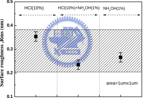
surface roughness is the same as two-step clean method. As shown in the Fig. 2-8, the GaAs surface roughness cleaned by different methods are between 0.354nm to.266 nm.
17
2-4 Summary
In this chapter, the suitable HCl and NH4OH solution both effectively clean GaAs substrate. These physical properties can be of enormous value to GaAs device. Finally, the optimum condition for HCl/D.I.W. solution is 10% at room temperature, effectively remove surface native oxide; the solution of
NH4OH/D.I.W.is 1% at room temperature, which remove As elemental and
arsenic oxide/gallium oxide ratio equal to one. If next chapter 3, we can use the cleaning method to develop surface treatment by sulfur solution, and the sulfur
passivation can improve the interface density (Dit) of high-k film on GaAs
substrate. The improved interface density can solve the Fermi level pinning, and the unpinned metal-oxide-semiconductor will come true.
18 1330 1328 1326 1324 1322 1320 1318 As2O5 N o rma lize d in te n sit y (a rb i. )
Binding energy (eV)
HCl:H2O=1:10 HCl:H2O=1:100 HCl:H2O2:H2O=1:1:10 As 2p3 As(GaAs) As-As As2O3 48 46 44 42 40 38 0.0 0.4 0.8 1.2 As-As As(GaAs) HCl:H2O=1:10 HCl:H2O=1:100 HCl:H2O2:H2O=1:1:10 As 3d N o rma liz ed in te n sit y (a rb i. )
Binding energy (eV)
As2O5 As2O3
Fig. 2-1 (a) As 2p and (b) As 3d core-level spectra with different diluted HCl concentration.
(a)
19 1124 1122 1120 1118 1116 1114 1112 0.0 0.4 0.8 1.2
Binding energy (eV)
Nor m al iz ed i n te ns it y(ar bi .) Ga 2O3 HCl:H 2O=1:10 HCl:H2O=1:100 HCl:H 2O2:H2O=1:1:10 Ga 2p3 Ga(GaAs) Ga2O 24 22 20 18 16 14 0.0 0.4 0.8 1.2
Binding energy (eV)
No rmalized intensi ty( arbi.) Ga 3d Ga2O3 HCl:H2O=1:10 HCl:H2O=1:100 HCl:H2O2:H2O=1:1:10 Ga(GaAs) Ga2O
Fig. 2-2 (a) Ga 2p and (b) Ga 3d core-level spectra after different diluted HCl concentration.
(a)
20 1330 1328 1326 1324 1322 1320 1318 HCl : H2O = 1:10,1Cycle HCl : H2O = 1:1,1 Cycle HCl : H2O = 1:1,8 Cycles As2O5 N o rm al iz ed i n te ns it y(ar bi .)
Binding energy (eV) As 2p3 As(GaAs) As-As As 2O3 1122 1120 1118 1116 1114 0.0 0.4 0.8 1.2 HCl : H2O = 1:10,1Cycle HCl : H2O = 1:1,1 Cycle HCl : H2O = 1:1,8 Cycles
Binding energy (eV)
N o rm al iz ed i n te ns it y(ar bi .) Ga2O3 Ga 2p3 Ga(GaAs) Ga2O
Fig. 2-3 (a) As 2p and (b) Ga 2p core-level spectra after different diluted HCl concentration and cleaned cycles.
(a)
21
Fig. 2-4 The fitting result of (a) As 2p and (b) Ga 2p core-level spectra after diluted HCl concentration. 1328 1326 1324 1322 1320 As-As As 2O5 As2O3 As2p3/2
Binding energy (eV)
Ph oto e lec tr o n inte ns ity (a rb .u nits ) As-Ga 1122 1119 1116 1113 Ga 2O3 Ga 2O Ga2p3
Binding energy (eV)
P h o to e le ctr o n in ten s ity (a rb .u nits ) Ga-As
(a)
(b)
22
Table 2-1 The fitting results of the GaAs component from photoelectron spectra.
Table 2-2 The fitting results of the GaAs component from photoelectron As 2p spectum .
Table 2-3 The fitting results of the GaAs component from photoelectron Ga 2p spectum .
Clean process A s oxide
/ G a oxide A s substrate /G a substrate A s total /G a total As O / A s total HCl:H2O=1:10 165% 37% 84% 14%
Position (eV) FWHM (eV) Area %Lorentzian - Gaussian(0:G,100:L) As (GaAs) 1322.75 1.75 419939.8 75
As-As 1323.77 1.8 150880.7 75
As2O3 1325.7 1.8 314532.4 70
AS2O5 1326.35 1.8 199913.2 80
Position (eV) FWHM (eV) Area %Lorentzian-Gaussian(0:G,100:L)
Ga (GaAs) 1117.25 1.8 780783.4 74
Ga2O 1118 1.8 122867.4 70
23 1329 1326 1323 1320 Ph otoelect ro n in te n s it y (ar b.un its)
Binding energy (eV) As 2p3 Raw data As-As
Fit curve As2O3 GaAs As2O5 (a) HCl (b) HCl_NH4OH (10% RT) (c) HCl_NH4OH (1% RT) (d) HCl_NH4OH (10% 80OC) 1329 1326 1323 1320
Fig. 2-5 The fitting results of As 2p core-level spectra with diluted HCl solution following by different NH4OH solutions.
Clean process A s oxide/
G a oxide A s substrate/ G a substrate As O / A s total A s total/ G a total HCl Clean 165% 37% 14% 84% HCl+NH4OH(10%,RT) 102.3% 36.6% 10.8% 64.2% HCl+NH4OH(1%,RT) 94% 38.6% 12.7% 59.4% HCl+NH4OH(10%,80oC) 124.1% 33.1% 12% 63.3%
Table 2-4 The ratio of GaAs component with diluted HCl solution following by different NH4OH solutions.
24 0.9 1.2 1.5 1.8 As o / As total As ox id e / Ga ox id e 0.12 0.15 0.18 1:10 (80OC) 1:100 (RT) 1:10 (RT) NH4OH conditions w/o
Fig. 2-6 The arsenic compound ratio with diluted HCl solution following by different NH4OH solutions.
25
Fig. 2-7 AFM image of cleaned GaAs substrate with different clean methods: (a)
HCl (b) HCl+NH4OH (c) NH4OH.
(a)
26 0.1 0.2 0.3 0.4 0.5 NH4OH(1%) HCl(10%) HCl(10%)+NH4OH(1%) Surface roughness ,Rms (n m) area=1umx1um
Fig. 2-8 Surface roughness of cleaned GaAs substrate with different clean
27
Chapter 3
The Sulfur Passivation on Gallium Arsenide Substrate
3-1 Introduction
It is well known that the high density of surface states and difficult task of
passivating them have been responsible for the slow development of GaAs MIS technology and other small geometry devices such as GaAs MESFETs, HBTs and HEMTs. Therefore, extensive effort has been expended over the past two decade to passivate the GaAs surface to realize GaAs MIS capacitors and MISFETs [31]-[45]. Among them, the sulfur chemical treatment of GaAs surface has received considerable attention because of its simplicity and suitability for commercial exploitation. Thus, even though a number of sulfur compounds such as Na2 S.9H2O [31]- [36] and (NH4 )2S [34]-[45]. In 1987, Sandroff was the first man to passivating the GaAs by sulfur using room-temperature Photoluminescence(PL) and low-temperature PL spectroscopy [31]. This can be attributed to the formation of native oxide on GaAs surface. It has been found that with the decrease in the solvent dielectric constant , in such solution the surface sulfur coverage increases , the thickness of the native oxide layer decreases, and the efficiency of band-edge
28
photoluminescence will increases [36]-[38]. The thermal stability of Ga-S bond is better than As-S bond. Annealing experimental show that As-S chemical bonds were broken at a relatively low temperature, approximately 200oC-300oC, whereas desorption of sulfur from the surface, through breaking of Ga-S bonds, occurs above 500 oC. At 500 oC-600 oC, only Ga-S remained stable, and the increasing density of sulfur from As to Ga atoms[39]-[44].Compared to the conventional basic (NH4)2S solution treatment, a thick Ga sulfur layer and Ga-S bond were formed on the GaAs surface after dipping GaAs in the neutralized (NH4)2S solution [45].
29
3-2 Experimental Procedure
The cleaning GaAs samples resulted from HCl and NH4OH-based solution
were immersed in sulfur solution for 1minute. Before immersing in sulfur solution, we dry the samples with N2 gas blowing to remove the excess surface moisture. This blowing can assure fewer effects during interface reaction between sulfur and semiconductor. We treat the cleaned samples with alcohol and deionized water-based sulfur-solvent solution, and adjust the sulfur concentration and temperature ramped from RT to 80oC by hot-plate machine to obtain the higher passivation efficiency. After sulfur passivation, we washed deionized water for 3minute to remove away the excess sulfur bond. Finally, dry
the samples with N2 gas to blow excess moisture. The sulfided samples
immediately were measured by X-ray Photoelectron Spectroscopy(XPS) and atomic force Microscopy(AFM) to get the surface chemistry and morphology .The electrical properties of sulfided samples were fabricated as metal-semiconductor device to calculate the Schottky barrier height, and we discuss passivation effect on barrier height. The gate electrode was 500nm Al deposited through a shadow mask to form a top electrode on the topside. The backside was 30nm indium(In) layer for ohmic contact and follow by 20nm platinum(Pt) layer for fast electric conductivity and protection. After backside
30
contact deposition, hot-plate with 90 oC and 10min was used to repair metal quality. A precision impedance meter of HP4284 was used for C-V measurement, and a semiconductor parameter analyzer of Keithley 4200 was used for I-V measurement.
31
3-3 Results and Discussion
3-3-1 XPS and PL of the sulfided GaAs substrate
The surface treatment of GaAs in sulfur solution results in a dramatic decrease surface state density in the middle of the band gap. Reduction of surface recombination velocity enables an improvement in the performance and reliability of many devices. For the beginning, three sulfur passivation methods were used to increase the efficiency on HCl-cleaned GaAs substrate, which was shown in the Figure 3-1.
First, Sodium sulfide is the salt of a strong base and a week acid, after its dissolution in D.I.W.:
2 2
2
Na S
+
H O
U
Na
++
HS
−+
OH
− (1)Second, Ammonium sulfide is the salt of a week base and a weak acid. In the D.I.W. reaction occurs:
2
4 3 4 3 2
2
NH
++
S
−U
NH
+
NH
++
HS
−U
2
NH
+
H S
(2)Both above sulfur coat formation can occur either by reaction (3) [37].
2 2
32
Finally, the organic twelve-carbon thiol with long-chain molecule type was used. The molecule was sulfur-terminated molecule which can be bonded with gallium or arsenic element of substrate. Fig. 3-1 shows the set of (a) As 2p and (b) Ga 2p core-level spectra after three sulfide treatment. The substrate peaks were normalized to the same height and substrate signals shifted to the same binding energy which was As(GaAs):1323 ± 0.5eV; Ga(GaAs):1117.5 ± 0.5eV. This study has taken a step in the direction of defining the relationship between sulfur and GaAs surface passivation in order to suppress the oxides. The sulfur signal also can be seen from the S 2p orbit spectra, as shown in the Fig. 3-2, and Fig. 3-2(a) points out the sulfur peak, which is overlap with Ga 3s peak, and the spacing about 1.1eV. Fig.3-2 (b) is the subtraction of S 2p and Ga 3s orbit, and we can subtract Ga 2s peak of no-sulfided sample from S 2p peak of sulfided one. The S 2p orbit can see the sulfur peak signal, but we don’t like to use this indirect way. The suppression of sulfided samples after 1week compared to no-sulfided one is shown in Fig. 3-3. Clearly, the sulfided sample can decrease the growth rate compared to no-sulfided one. Hence, the sulfur passivation for GaAs substrate is useful and further research is required. There are two sulfur methods with PL analysis as shown in Fig. 3-4 and Fig. 3-5. The Fig. 3-4(a) is the Photoluminescence(PL) intensity treated by (NH4)2S/D.I.W.
33
liquid. It shows that sulfided temperature increasing the PL intensity before 400 o
C, and it decreases at 500 oC. This is because arsenic bonds fully broke before 400 oC, and Ga compound bonds began to desorb. Then, the solvent effect was replaced with C3H7OH solution, whose results were shown in Fig.3-4(b). When anneal at 400oC and highest concentration with 10% will obtain the highest PL intensity. The highest PL intensity cause may be the more sulfur bond coverage.
The Fig. 3-5 is the Photoluminescence(PL) intensity treated by Na2S/D.I.W.
liquid . Fig. 3-5(a) shows that sulfided temperature increasing the PL intensity at 400oC, and it decrease at 500 oC. Then, the solvent was chosen with C3H7OH solution, whose results were shown in Fig.3-5(b). When the PDA anneal at 400 o
C, highest concentration with 2.5% will increase PL intensity.
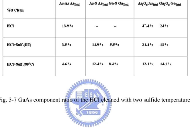
Fig. 3-6(a) and (b) illustrate XPS spectra of the sulfide temperature effect. When the temperature is increasing, the Ga-S bonds will increase and As-S bonds decrease. This is because that thermal stability of Ga-S bonds is better than As-S bonds. Fig.3-7 shows different ratio of GaAs surface signal, and we divide into five parts: (i) As element (ii) As-S (iii) Ga-S (iv) As-O (v) Ga-O. After sulfidation, the As element decrease from 13.9% to 3.5%, and oxides decrease one half at least. About sulfur composition, the high sulfided temperature causes the Ga-S bonds increasing compared to As-S bonds
34
decreasing. Fig.3-8 (a) and (b) are spectra of GaAs with two sulfur concentration, we believe that sulfur really suppresses the GaAs oxide under 80oC passivation solution. Fig. 3-9 (a) and (b) are sulfur concentration at Ga orbit spectra. They also show the same behavior compared to Fig. 3-8. In the Fig. 3-10(a) and (b),
we discuss the alkaline NH4OH solution effect combining with sulfur
passivation on the GaAs surface. From the Fig. 3-10 (a), we find the As element peak magnitude of (i) and (ii) are different. With NH4OH solution cleaned, the As element component will decrease, because of As(OH) bonds can remove easily compared to Ga(OH) bonds. When sulfided temperature increase, the As-O and As element both expressed decreasing behavior. Fig. 3-10 (b) is the
Ga 2p spectrum, we find that the Ga-S peak increase with 80oC sulfur
temperature compared to RT treatment. The Ga element likes to react with sulfur solution at high temperature. Simply stated, the NH4OH solution etching can reduce As compound bonds and get a Ga-termined surface .Fig. 3-11 shows different ratio of GaAs surface signal, and we divide into five parts: (i) As
element (ii) As-S (iii) Ga-S (iv) As-O (v) Ga-O. After NH4OH and sulfur
solution, the As element decrease from 9.6% to 4.7%, and oxides also decrease. About sulfur composition, the high sulfide temperature cause the Ga-S bonds increase .On the other hand, As-S bonds decrease with high sulfided
35
temperature.
3-3-2 surface roughness of the sulfided GaAs
Fig. 3-12 shows the variation of surface roughness of GaAs after the cleaning of diluted HCl/D.I.W. (10%) etching solution with three sulfide
conditions of (a) without (b) 1%, RT (c) 1%, 80oC.The surface roughness
decrease as sulfide temperature increase from 0.354nm to 0.237nm. Fig. 3-13 shows the variation of surface roughness of GaAs after the cleaning of diluted
HCl/D.I.W.(10%) and NH4OH/D.I.W.(1%) etching solution with two sulfide
conditions of (a) without (b) 1%, 80oC. The surface roughness ranges from
0.265nm to 0.235nm. Fig. 3-14 shows the variation of surface roughness of
GaAs after the cleaning of diluted NH4OH/D.I.W.(1%) etching solution with
two sulfide conditions of (a) without (b) 1%, 80oC. The surface roughness
ranges from 0.266nm to 0.245nm. All the variation of surface roughness after different treatment is summarized in Fig.3-15, and the GaAs surface roughness is smooth with different surface treatment.
36
3-3-2 electrical characterization of the sulfided GaAs
In Fig. 3-16, we treatment the HCl cleaned GaAs substrate with two sulfur solutions combined with three solvents. The curves were measured at room temperature, and we find that the I-V curves depend on surface treatment. As displayed in Fig. 3-17 was the extraction of Schottky barrier height(SBH) by following equation: (1) * 2 s
Where J =A T e
B q kT − Φ, A* is the Richardson constant; n is the ideal
factor;
Φ
Bis the barrier height. Fig. 3-18 and 3-19 show the variationof barrier height with different sulfide treatment. Because that the ideal barrier height difference of Al metal contact to n-GaAs substrate is about 0.4 eV, and the barrier height of sulfided GaAs is smaller than no-sulfidation one. From the Fig. 3-19, the barrier height decreased with decreasing dielectric constant of solvent solution. This is because that efficiency for different solvents solution. Fig. 3-20 shows I-V curves difference before and after sulfidation, and we find that original Schottky-like diode curve has change to ohmic-like curve.
-qV/nkT s
37
3-4 Summary
After sulfur passivation, the GaAs surface elements bond with sulfur
element. The formation of As-S or Ga-S bond depends on clean method and sulfided temperature. The HCl etching solution remains the As-terminated surface, but NH4OH remains the Ga-terminated surface. We can use the sulfided temperature to mathch with GaAs surface element. Because of thermal stability for As-S bonds are worse better than Ga-S bonds. We need to increase the sulfided temperature up to 80oC, and Ga-S bonds remain stable. The Schottky barrier height (SBH) can be changed to ideal-like value by sulfidation, especially in solvent solution.
37 1332 1330 1328 1326 1324 1322 1320 0.0 0.4 0.8 1.2 1.6
Binding energy (eV)
As-S N o rm a lize d In tensity (ar b . un it) control sample (NH4)2S treatment Na2S treatment 12C-Thiol treatment As 2p 3 As(GaAs) As-O (a) 1122 1120 1118 1116 1114 1112 0.0 0.4 0.8 1.2 1.6 (b)
Binding energy (eV)
N orm a liz ed Inte n s ity (ar b. un it) Ga-S Ga-O control sample (NH4)2S treatment Na2S treatment 12C-Thiol treatment Ga2p 3 Ga(GaAs)
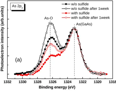
Fig. 3-1 (a) As 2p and (b) Ga 2p core-level spectra after different sulfide methods.
38
Fig. 3-2 (a) S 2p spectra by three sulfur passivation before subtraction and (b) after subtraction Ga 2s peak from S 2p peak.
170 168 166 164 162 160 158 156 154 152
As-S/Ga-S
Intensi
ty
Binding energy (eV)
No Sulf. (NH4)2S treat. Na2S treat. 12C-Thiol treat. S2p3 &Ga3s overlap (a) 170 168 166 164 162 160 158 156 154 152 (b) Intensi ty
Binding energy (eV)
(NH4)2S treat. Na2S treat.
39 1332 1330 1328 1326 1324 1322 1320 1318 (a) P h oto e le c tro n in te ns ity (a rb .u nits )
Binding energy (eV)
w/o sulfide
w/o sulfide after 1week with sulfide
with sulfide after 1week As 2p3 As(GaAs) As-O 1122 1120 1118 1116 1114 1112 (b) P h o toe le ctr o n inte n s ity (ar b .un it)
Binding energy (eV)
w/o sulfide
w/o sulfide after 1week with sulfide
with sulfide after 1week
Ga 2p
3 Ga(GaAs)
Ga-O
Fig. 3-3 (a) As 2p and (b) Ga 2p core-level spectra of the sulfided samples against moisture with spectra after 1week .
40
10000 15000 sulf. 27oC + 500oC anneal sulf. 27oC + 400oC anneal sulf. 70oC sulf. 27oC PL Intensity (a.u.) w/o sulf. (a) (NH 4)2S (aq.)=1:40 10 15 20 25 0 10000 20000 30000 40000 50000
(b)
PL measurement time (sec)
Inte nsity (a .u.) No treat. 1:10 1:40 1:80 (NH4)2S : C3H7OH ratio with 400oC RTA
Fig. 3-4 Photoluminance of Gd2O3/ GaAs sulfided by (NH4)2S solution with different (a) temperature and (b) concentration.
41 0 50 100 150 200 250 300 0 100000 200000 300000 400000 500000 No anneal 400oC anneal 500oC anneal
PL measurement Time (sec)
Intensity (a.u.) Na 2S(aq.)=1:40
(a)
0 50 100 150 200 250 300 0 100000 200000 300000 400000 500000(b)
1:10 1:20 1:40PL measurement Time (sec)
Intensity (a.u.)
Na2S(aq.) ratio with 400oC anneal
Fig. 3-5 Photoluminance of Gd2O3/ GaAs sulfided by Na2S solution with different (a) temperature and (b) concentration.
42
Fig. 3-6 (a) As 2p (b) Ga 2p core-level spectra of sulfided GaAs at various treatment temperature: (i) without sulfide (ii) sulfide at room temperature (iii) sulfide at 50oC (iv) sulfide at 80oC.
1330 1328 1326 1324 1322 1320 1318
(iii) 80OC Sulfide
Raw data As-As Fit curve As-S GaAs As2O3 As2 O5 (ii) RT Sulfide (i) control P h o to e le ctr o n in ten s ity (a rb .un its )
Binding energy (eV)
As2p3 (a) 1122 1120 1118 1116 1114 1112 (iii) 80oC Sulfide (ii) RT Sulfide (i) control Ph ot oe lec tro n i nt e ns it y ( arb. u ni ts )
Binding energy (eV)
(b) Raw data Fit curve Ga-SGa2O
GaAs Ga2O2
43
44 1330 1328 1326 1324 1322 1320 1318 (iii) 2% Sulfide Raw data As2O3 Fit curve As2O5 As-As As-S GaAs (ii) 0.5% Sulfide (i) control Ph o toe lec tr o n inte ns ity (a rb .u nits )
Binding energy (eV)
As2p3 (a) 46 44 42 40 38 (b) As 3d control sample 0.5% Sulfide 2% Sulfide
Binding energy (eV)
P h o to e le ctr o n in ten s ity (a rb .u nits ) AsOx As-As As-S As-Ga
Fig. 3-8 (a) As 2p and (b) As 3d spectra of GaAs after two sulfur concentration: (i) cleaned (ii) sulfide at 0.5% concentration (iii) sulfide at 2% concentration.
45 1122 1120 1118 1116 1114 (iii) 2% Sulfide (ii) 0.5% Sulfide (i) control P ho toel e ct ron i n ten si ty ( a rb .uni ts )
Binding energy (eV)
Raw data GaOX Fit curve Ga-S GaAs Ga2p3 (a) 22 21 20 19 18 17 control 0.5% Sulfide 2% Sulfide
Binding energy (eV)
Ph o toe lec tr o n in ten s ity (a rb .un its) Ga3d GaOX Ga-S Ga-As (b)
Fig. 3-9 (a) Ga 2p and (b) Ga 3d spectra of GaAs after two sulfur concentration: (i) cleaned (ii) sulfide at 0.5% concentration (iii) sulfide at 2% concentration.
46 1330 1328 1326 1324 1322 1320 1318 (iii) HCl_NH4OH_ Sulfide(80oC) (a) Raw data As2O3 Fit curve As2O5 GaAs As-As As-S (ii) HCl_NH4OH _Sulfide(RT) (i) HCl_Sulfide(RT) P h o to e le ctr o n in ten s ity (a rb .u nits )
Binding energy (eV)
As2p3 1122 1120 1118 1116 1114 1112 (iii) HCl_NH4OH _Sulfide(80 o C) (ii) HCl_NH4OH _Sulfide(RT) (i) HCl _Sulfide(RT) P h o to e le ctr o n in ten s ity (a rb .u nits )
Binding energy (eV)
(b) Raw data Fit curve GaAs Ga-S Ga2p3
Fig.3-10 (a) As 2p and (b) Ga 2p core level spectra after HCl+NH4OH solution with two sulfided temperature.
47
Fig. 3-11 GaAs component ratio of the HCl、NH4OH solutions cleaned with two
48 HCl(10%) Rms (Rq) 0.354nm HCl(10%) +Sulfide(1%,RT) Rms (Rq) 0.296nm HCl(10%) +Sulfide(1%,80oC) Rms (Rq) 0.237nm (a) (b) (c)
Fig. 3-12 Surface morphology of HCl cleaned GaAs substrate after different sulfide condition: (a) without sulfidation (b) 1%, RT (c) 1%, 80oC.
49 Rms (Rq) 0.265nm HCl(10%) + NH4OH(1%) HCl(10%) + NH4OH(1%) + Sulfide(1%,80oC) Rms (Rq) 0.235nm (a) (b)
Fig. 3-13 Surface morphology of HCl +NH4OH cleaned GaAs substrate after
50
Rms (Rq) 0.266nm
NH4OH(1%) NH4OH(1%)+Sulfide(1%,80oC)
Rms (Rq) 0.245nm
Fig. 3-14 Surface morphology of NH4OH cleaned GaAs substrate after different sulfide condition: (a) without sulfidation (b) 1%, 80oC.
51 0.1 0.2 0.3 0.4 0.5 w/o w/o (1%,80OC) NH4OH(1%) HCl(10%) HCl(10%)+NH4OH(1%) Su rf a c e ro u g hn es s , R ms ( n m) area=1umx1um (1%,80OC) (1%,80OC) (1%,RT) Sulfide conditions w/o
52
Fig. 3-16 I-V curves of Al metal contact to n-GaAs substrate with different surface treatment.
Fig. 3-17 Extraction of Schottky barrier height(SBH) with Al metal on n-type GaAs -1.0 -0.8 -0.6 -0.4 -0.2 0.0 0.2 0.4 0.6 0.8 1.0 1E-8 1E-7 1E-6 1E-5 1E-4 1E-3 0.01 0.1 1 10 100 1000 Applied Voltage (V) Current densit y (A/ cm 2 ) No treatment (NH4)2S:H2O (NH4)2S:C3H7OH (NH 4)2S:C4H9OH Na 2S:C3H7OH Na2S:C4H9OH Al / n-GaAs(100) 0.00 0.05 0.10 0.15 0.20 1E-7 1E-6 1E-5 1E-4 1E-3 0.01 0.1
J
(
A/c
m
2)
Forward Voltage (V)
J/(1-e-qV/kT) Al / n-GaAs(100)J
J
S53
Fig. 3-18 Schottky diode parameters with (NH4)2S solution after (i) no-anneal (ii) 400oC N2 anneal (iii) 500
o
C N2 anneal.
Fig. 3-19 Schottky diode parameters with sulfur solution and different solvents: (i) H2O (ii) C3H7OH (iii) C4H9OH.
54
Fig. 3-20 Schottky barrier height(SBH) with sulfur solution and different solvents : (i) H2O (ii) C3H7OH (iii) C4H9OH.
Fig. 3-21 I-V curves of Schottky diode (a) with and (b) without sulfide.
0.55 0.60 0.65 0.70 0.75 0.80 1/ dielectric constant (10-2) 5 Al / n-GaAs
Barrier height (eV)
(NH 4)2S+C3H7OH (NH4)2S+H2O No treat. Na2S+C3H7OH Na2S+C4H9OH (NH4)2S+C4H9OH 1.25 8 -0.9 -0.6 -0.3 0.0 0.3 0.6 0.9 1E-9 1E-8 1E-7 1E-6 1E-5 1E-4 1E-3 0.01 0.1 1 Ohmic contact Applied voltage (V) w/o sulfide with sulfide Cu rr ent ( A ) Al/n-GaAs(100) Schottky contact
55
Chapter 4
Electron-beam evaporated Gd
2O
3Gate
Dielectric On GaAs Substrate
4-1 Introduction
In recent years, high-k gate dielectrics on Si substrate have been proved being able to significantly reduce the leakage currents as compared to the
traditional SiO2/Si system, while still maintain excellent reliability and
high-level of transistor performance. In order to further enhance device driving capability, GaAs is a great potential semiconductor material due to its higher electron mobility for carrier transport. Interestingly, the lack of sufficiently stable native GaAs oxide makes the integration of high-k gate dielectric on top of GaAs substrate receive more and more attentions. Up to now, several metal oxides, e.g., Al2O3 [46], Ga2O3 [47] showed high breakdown field and sharp interface in atomic scale with low interface state density with n-GaAs substrate. Epitaxial growth of single-crystal gadolinium oxide dielectric thin films om GaAs is reported [48]. Ultrathin Gd metal was evaporated on GaAs surface covered with native oxides, and the oxides could be reduced during the deposition of Gd metal [49]-[50].By directly evaporated Gd2O3 oxide on GaAs
56
substrate to keep a stable interface [51]-[54]. In our work, we systematically investigated the impact of surface treatment on the electrical and material properties of Gd2O3 dielectric on the GaAs substrates.
4-2 Experimental Procedure
The real time cleaning GaAs samples result from HCl and NH4OH-based were immersed in sulfur solution, before immersing in sulfide solution, we dry
the samples with N2 blowing to remove the excess surface moisture. This
blowing can assure the less causes during interface reaction between sulfur and semiconductor. We treat the immediate samples with (NH4)2S liquid solution, we also adjust the sulfur concentration and temperature to obtain the higher efficiency. After sulfur passivation, we washed deionized water for 3min to wash away the excess sulfur bond. Finally, dry the samples with N2 blowing.
The Gd2O3 film was deposited on the GaAs substrate by e-beam evaporation
from a source under 4×10⁻⁶ torr at room temperature. The deposition rate of
0.05nm /s was calibrated using a quartz-crystal. The post-dielectric anneal (PDA)
with O2/Armixed gas and 25 torr vacuum ambient was performed to improve
the Gd2O3 film quality and electrical characteristics. The accomplished Gd2O3 film samples were measured chemical composition detected by X-ray