行政院國家科學委員會專題研究計畫 成果報告
金屬-鐵電-絕緣-半導體場效應電晶體之開發研究
研究成果報告(精簡版)
計 畫 類 別 : 個別型 計 畫 編 號 : NSC 97-2221-E-009-014- 執 行 期 間 : 97 年 08 月 01 日至 98 年 10 月 31 日 執 行 單 位 : 國立交通大學電子工程學系及電子研究所 計 畫 主 持 人 : 邱碧秀 計畫參與人員: 碩士班研究生-兼任助理人員:吳杼樺 博士班研究生-兼任助理人員:鄧至剛 報 告 附 件 : 出席國際會議研究心得報告及發表論文 處 理 方 式 : 本計畫可公開查詢中 華 民 國 99 年 02 月 01 日
行政院國家科學委員會補助專題研究計畫
■ 成 果 報 告
□期中進度報告
金屬-鐵電-絕緣-半導體場效應電晶體之開發研究
計畫類別:■ 個別型計畫 □ 整合型計畫
計畫編號:NSC 97-2221-E-009-014-
執行期間: 97 年 8 月 1 日至 98 年 10 月 31 日
計畫主持人:邱碧秀 教授
共同主持人:
計畫參與人員:鄧至剛、吳杼樺
成果報告類型(依經費核定清單規定繳交):■精簡報告 □完整報告
本成果報告包括以下應繳交之附件:
□赴國外出差或研習心得報告一份
□赴大陸地區出差或研習心得報告一份
■出席國際學術會議心得報告及發表之論文各一份
□國際合作研究計畫國外研究報告書一份
處理方式:除產學合作研究計畫、提升產業技術及人才培育研究計畫、
列管計畫及下列情形者外,得立即公開查詢
□涉及專利或其他智慧財產權,□一年□二年後可公開查詢
執行單位:國立交通大學電子工程學系及電子研究所
中 華 民 國 九十九 年 一 月 三十一 日
I
中文摘要
在這個研究中,我們使用高介電常數的三氧化二鑭絕緣層,來製作金屬-絕緣層-金屬 (金氧金)電容測試結構。然後深入探究其操作原理,和實際應用面上所產生的問題,包含 漏電流和其傳導機制、類比特性和其訊號失真機制、受電應力行為和劣化過程,以及介電 絕緣層崩潰和可靠度特性探討等,以發展出適用於金屬-鐵電-絕緣-半導體場效應電晶體的 良好絕緣層。根據實驗結果可歸結出,十奈米三氧化二鑭金氧金電容,其具有低漏電流(在 外加電壓−1 V 時為 9.4 nA/cm2),很高的崩潰電場 (在 25 °C 時大於 7 MV/cm),低的電容 電壓係數(頻率在 100 kHz 時為 671 ppm/V2),足夠高之電容密度(11.4 fF/μm2),以及高度 穩定性和良好的可靠度等眾多優良特性。因此,鑭系高介電常數絕緣層在金屬-鐵電-絕緣-半導體場效應電晶體的應用上極具潛力。 關鍵字: 高介電常數,三氧化二鑭,金屬-絕緣層-金屬(金氧金)測試結構,金屬-鐵電-絕 緣-半導體場效應電晶體英文摘要
In this study, the metal-insulator-metal (MIM) test structure with the high dielectric constant (high-k) lanthanum oxide (La2O3) film was fabricated and characterized. In order to develop good
insulator suitable for Metal-Ferroelectric-Insulator-Semiconductor Field Effect Transistor (MFIS-FET), the operational principles and the implementation issues of the high-k La2O3 MIM
capacitor are discussed, including leakage current and conduction mechanisms, analog properties and distortion mechanisms, stress behaviors and degradation processes, as well as dielectric breakdown and reliability characteristics. In summary, according to the experimental results, a highly stable and reliable 10-nm La2O3 MIM capacitor with low leakage current (9.4 nA/cm2 at
−1 V), high breakdown strength (> 7 MV/cm at 25 °C), small VCC (671 ppm/V2
at 100 kHz), and sufficient high capacitance density (11.4 fF/μm2
) has been successfully demonstrated. The results highlight the promise of the La-based high-k dielectrics as the insulator of MFIS-FET.
Keywords: high dielectric constant (high-k), lanthanum oxide (La2O3), metal-insulator-metal
(MIM) test structure, Metal-Ferroelectric-Insulator-Semiconductor Field Effect Transistor (MFIS-FET)
1
一、前言及研究目的
隨著資訊產業膨渤發展與資訊媒體應用的日益普及,各類的資訊儲存器也就日形重 要。其中電子記憶體無疑是最重要的一種。目前電子記憶體依功能主要可分為兩類,一類 是強調高速存取的隨機記憶體(Random Access Memory, RAM),其讀寫速度可在100 奈秒 (ns)以下,但卻沒有永久記憶的功能。另一類則為非揮發性(Nonvolatile)的唯讀記憶體 (ROM),強調永久記憶的功能,但資料寫入的速度卻須微秒(μs)以上的時間。無法同時具備 兩種功能,使得電子記憶體在應用上受到頗多限制。而鐵電薄膜的高介電係數,可應用於 動態隨機記憶體,而高自發極化值則可應用於非揮發性記憶體,鐵電材料的引入為電子記 憶體的發展另闢一個新的方向。。近年來由於薄膜製程技術的進步,已可在矽晶上製作出 高品質的鐵電薄膜,使得它在產業的應用上受到極大重視。第一個由金屬-鐵電-半導體 (Metal Ferroelectric Semiconductor, MFS)所構成的元件則是由吳泗堯(S.-Y. Wu)博士於1974 年所發表[1],其金屬-鐵電-半導體電晶體(Metal-Ferroelectric-Semiconductor Field Effect Transistor, MFIS-FET)基本的操作物理模型為Miller和McWhorter建立[2]。此元件結構與標準 的金屬-絕緣體-半導體(Metal Insulator Semiconductor, MIS)相似,只不過絕緣體被鐵電薄膜 所取代,不過由於鐵電薄膜與半導體的介面並不穩定,在操作過程中電荷會從矽晶表面穿 過原始氧化層而陷於鐵電薄膜表面,因此元件並未能真正發揮功效。此種記憶體由於在元 件製作過程中,鐵電薄膜與半導體之間容易有元素相互擴散的問題,直接影響閘極通道狀 態,因此成為發展上最大的障礙。 為了要改善鐵電材料和半導體矽的接面品質,因此有許多論文開始在中間加入緩衝絕 緣層來改善介面特性,使用CaF2 [3]和Al2O3 [4] 緩衝絕緣層在金屬-鐵電-絕緣-半導體電容 結構上,以及使用MgO [5]和SiO2 [6]緩衝絕緣層在金屬-鐵電-絕緣-半導體電晶體結構上。 雖然加入緩衝絕緣層後能改善接面特性,然而卻無法延長儲存在鐵電層中的極化電荷 (Polarization Charge, F P )的保存時間(Retention Time),以致於此金屬-鐵電-絕緣-半導體場 效應電晶體領域仍處於研究發展階段,無法大量生產運用於工業界的產品上面。已有論文 [7]特別指出兩種原因對極化電荷的保存時間影響的重要性,其一為在鐵電材料層所自我產 生的極化電場(Depolarization Field, Edp)效應[8],其二為閘極漏電流的影響[9],此兩種因素 會隨時間的增長,漸漸地抵銷鐵電材料內所儲存的極化電荷,使得極化電荷對通道的影響 力消失,無法維持記憶體的特性。其中極化電荷( F P )是外界施加電壓寫入後造成的,如果 要降低極化電場的影響力,唯有從提高絕緣層的電容值下手,即是選取具有高介電係數的 絕緣材料,才能降低極化電場(Edp)效應的影響。而為了減少漏電流的注入效應,最直接的 方法就是增加絕緣層厚度(ex: >10 nm) [10], [11],來降低跨在絕緣層上的電場,然而持續增 加了絕緣層厚度會造成絕緣層的電容值變小,當電容值變小時,極化電場(Edp)會因此增 加,而又會隨時間增加漸漸地抵銷鐵電材料內所儲存的極化電荷( F P ),因此這兩者效應是 互相抵制。所以減少閘極漏電流的第二種方法,就是從選擇高矽和絕緣層價帶(或導帶)的能 帶差的高介電絕緣層下手[12]。電晶體在操作區間內的漏電流不能大於10 μA/cm2,如此的 漏電流才能維持極化電荷不被漏電流中和,造成降低金屬-鐵電-絕緣-半導體電晶體的記憶 特性和減少記憶開口的電壓。此外極化電荷量和絕緣層的介電常數有很大的關係,選擇越 高介電常數的絕緣層,才能產生更大的極化電荷量,使金屬-鐵電-絕緣-半導體電晶體符合 鐵電的電滯曲線操作。為了要維持金屬-鐵電-絕緣-半導體電容系統的電中性,在操作上能 承受電滯曲線上的電荷量,除了選擇高介電係數的絕緣層外,在使鐵電層經過矯頑電場的
2
施加後產生極化電荷儲存的狀態,絕緣層也需具有可耐高的電場( ~ 4 MV/cm),在此電場的
操作下漏電流小於10 μA/cm2,如此的漏電流位準為一般記憶體最低要求。
因此,本研究計畫目的在開發整合良好的高介電係數絕緣層在金屬-鐵電-絕緣-半導體
電晶體的應用。根據文獻上的報導,三氧化二鑭(La2O3)緣層具有大的能隙(Energy Bandgap >
5 eV) [13],相對高的介電常數(20-30) [13], [14], [15],高崩潰電場[16],低的界面態密度 (interface state density) [13], [14],低漏電流[13], 好的絕緣層可靠度[17]等眾多優點。是故在 這個研究中,我們使用高介電常數的三氧化二鑭絕緣層,來製作金屬-絕緣層-金屬(金氧金) 電容測試結構。然後深入探究其操作原理,和實際應用面上所產生的問題,包含漏電流和 其傳導機制、類比特性和其訊號失真機制、受電應力行為和劣化過程,以及介電絕緣層崩 潰和可靠度特性探討等,以發展出適用於金屬-鐵電-絕緣-半導體場效應電晶體的良好絕緣 層。
二、研究方法
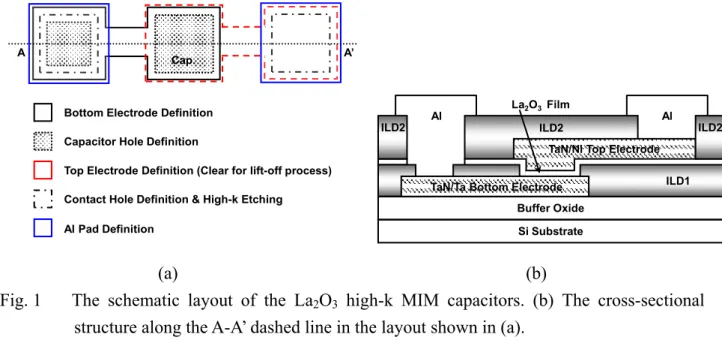
The schematic layout and its cross section along the A-A’ line of the fabricated La2O3 MIM
capacitors are shown in Figs. 1(a) and 1(b), respectively. The main fabrication steps were summarized below.After performing the standard RCA clean process to remove the native oxide and any contamination, the 1-µm thermal oxide was grown on 6-inch Si wafer as an isolation buffer layer by using wet oxidation. And then, the 200-nm tantalum (Ta) layer and the 50-nm tantalum nitride (TaN) layer were subsequently deposited on buffer oxide layer as the bottom electrode by a reactive sputtering system. Ta layer and TaN layer were used to reduce the parasitic resistance and to serve as a diffusion barrier layer, respectively. Before defining the bottom electrode of the MIM capacitor, the surface of TaN was treated by ammonia (NH3) plasma
nitridation at 300 mtorr with the RF power of 100 watts for 10 minutes to reduce the interfacial layer during the following high-k annealing processes. Besides, the metal layer TaN with NH3
treatment has more flat surface roughness so that the leakage current of the MIM capacitor could be reduced under bottom injection condition.
The bottom electrode TaN/Ta was lithographically patterned and defined by employing a transformer-coupled-plasma (TCP) etcher with chlorine-based gas. Subsequently, the 200-nm tetraethoxylsilane (TEOS) oxide film used as the first inter-layer dielectric (ILD) isolation was deposited by utilizing a plasma-enhanced chemical vapor deposition (PECVD) system at 300 °C. The capacitor region and the bottom contact region were etched by buffered oxide etchant (BOE) solution after being opened by optical lithography process. Afterwards, the lanthanum oxide (La2O3) was deposited by using electron beam evaporation. The high-k dielectric La2O3 film on
bottom electrode was annealed at 400 °C in O2 ambient to improve its quality via fully oxidation
and defects elimination. After lithography process to define the top electrode region, the 60-nm nickel (Ni) and the 30-nm TaN were subsequently deposited by electron beam evaporation and reactively sputtering, respectively. And then, the top electrode with Ni/TaN bi-layer metal was formed by using lift-off technique.
Next, the 300-nm TEOS oxide film served as the second ILD passivation layer was deposited by using a PECVD system at 300 °C. Because the La2O3 high-k dielectric film and the
3
etching process for interconnection. Firstly, the 300-nm ILD passivation on contact hole region was removed by BOE solution and its could be etched, and the etching process could be stopped on the top of the TaN electrode and the La2O3 film. Secondly, the mixed solution of H3PO4:
HNO3: CH3COOH: H2O = 50: 2: 10: 9 heated to 60 °C was used to dissolve La2O3 film with high
etching selectivity to the ILD passivation layer and the TaN electrodes. After the contact holes were opened by two-step wet etching process, the aluminum (Al) film of 500 nm was deposited by using a thermal evaporation system. Finally, the aluminum pads were lithographically patterned and also etched by the mixed solution of H3PO4: HNO3: CH3COOH: H2O = 50: 2: 10: 9
at 60 °C. Ultimately, the MIM capacitors with La2O3 high-k dielectrics were accomplished. It was
noteworthy that the maximum temperature during MIM capacitors fabrication was 400 °C, which was compatible with VLSI backend process.
An automatic measurement system consisted of a person computer (PC), Agilent-4156C, Agilent-4284A, Agilent switch, and a probe station is used for DC and low-frequency measurement of the fabricated devices. The properties of the La2O3 MIM capacitor are measured
by the temperature-controlled chuck of the probe station, such as leakage current, capacitance density, breakdown biased voltage, and reliability characteristics. For all of electrical measurements, the voltage and the altering signal are applied to the top electrode while the bottom electrode was grounded. The leakage current-voltage (J-V) measurements are preformed on the Agilent-4156C semiconductor parameter analyzer. The capacitance-voltage (C-V) curves are measured by the Agilent 4284A precision impedance meter, and the dielectric loss-voltage (D-V) curves could also be observed at the same time. The biased voltage on the top electrode of the La2O3 MIM capacitor sweeps from −2 V to 2 V at frequencies varying from 10 kHz to 500
kHz by applying an ac signal with 25-mV amplitude. Moreover, from the viewpoint of practical use, it is very important to clarify the stability of MIM capacitor properties during long-term voltage stress. Therefore, the constant voltage stress (CVS) in the range of −4 V to −5 V at the temperature of 25°C is conducted by utilizing the Agilent-4156C semiconductor parameter analyzer. The C-V and J-V characteristics of La2O3 MIM capacitors are also measured at various
time intervals during CVS testing.
A’ A
Cap.
Bottom Electrode Definition Capacitor Hole Definition
Top Electrode Definition (Clear for lift-off process) Contact Hole Definition & High-k Etching Al Pad Definition
(a)
Buffer Oxide Si Substrate
ILD1 TaN/Ni Top Electrode
ILD2 ILD2
ILD2 Al Al
TaN/Ta Bottom Electrode
La2O3 Film
(b)
Fig. 1 The schematic layout of the La2O3 high-k MIM capacitors. (b) The cross-sectional
4
三、結果與討論
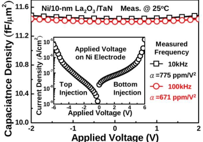
Figure 2 shows the C-V and J-V characteristics of the 10-nm La2O3 MIM capacitor. The
capacitance density at zero bias is about 11.4 fF/µm2, and the leakage current densities at −1.5 and +1.5 V are 16 and 56 nA/cm2, respectively. The quadratic voltage coefficient of capacitance (α), used to depict the voltage dispersion or voltage dependency of capacitance, is obtained from fitting the C-V curves by the second-order polynomial equation:
( )
(
2)
0 1
= × × + × +
C V C α V β V , (1)
where C0 is the capacitance at zero bias. The α values of the 10-nm La2O3 MIM capacitor
measured at 10 and 100 kHz are 775 and 671 ppm/V2, respectively. The positive α represents a capacitance density rise with the increase in applied voltage, which may be attributed to the high degree of electric field polarization and carrier injection. During the voltage sweeping, some of the injected carriers would be captured by the interface trap states existing in the dielectric near the injection electrode. These trapped charges could induce dipoles following the alternating signals with a dipole relaxation time. Moreover, the other injection carriers become excess mobile charges in the insulator, and these mobile charges also follow the small ac signals with a free carrier relaxation time that depends on the mobility and density of carriers. The dipole and free carrier relaxation time contribute to various frequency-dependent characteristics in RF/analog MIM capacitors. As the measurement frequency increases, the trapped-charge-induced dipoles and the excess mobile charges hardly follow the ac signal, corresponding to the longer relaxation times of these dipoles and mobile charges. Thus, the capacitance fluctuation due to the varied applied voltages becomes smaller and results in the lower α with increasing frequency. While both dipole polarization and free carrier polarization could modulate the capacitance, the free carrier effect is believed to play the major role in the voltage dependence of capacitance, but is negligible for the zero-biased capacitance where the carrier injection ceases.
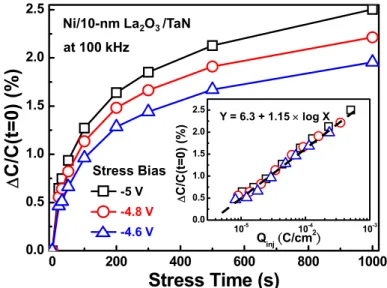
To further investigate the stability of the La2O3 MIM capacitor under electrical stress, the
CVS test was carried out. Figure 3 shows the relative capacitance variation [ΔC/C(t=0)] as a function of stress time at various CVS voltages from −4.6 to −5 V. The relative capacitance variation is defined as
(
)
0( )
0(
0(
)
)
0 0 0 − = Δ = = = C t C t C C t C t , (2)where C0(t=0) is the initial capacitance at zero bias before stress, and t is the stress time.
[ΔC/C(t=0)] increases with the CVS voltage and the stress time. On the other hand, [ΔC/C(t=0)] is also plotted as a function of the injected charge (Qinj) in the inset of Fig. 3. The relative
capacitance variation increases with a logarithmic increase in Qinj regardless of the stress biases,
which implies that the increasing charge trapping in dielectrics during CVS is responsible for the capacitance variation. The trapped charges in the preexisting traps and in stress-induced traps generate dipoles to increase the local permittivity and the capacitance. Among them, the stress-induced dipoles contribute to the relative increase in capacitance with respect to its initial
5
condition, and that is the degradation of the capacitance. Specifically, the relative capacitance variation is proportional to the amount of stress-induced trapped charges. Furthermore, the trapping probability, the ratio of trapped charge variation, ΔQtrap, to injected charge variation,
ΔQinj, obeys a power law relation:
Δ = × Δ trap n inj inj Q K Q Q , (3)
where K is the trapping efficiency as a function of the injected current density and the temperature, and the characteristic exponent n is a fraction. As a consequence, the logarithmic dependence of the relative capacitance variation on the injected charge is shown in the inset of Fig. 3. Moreover, the CVS conditions presented here exhibit a nearly linear relationship between Qinj and stress time (not shown). The power law behavior of trapping probability brings about the
slower increase in capacitance after long-term stress. Both the linear relationship between [ΔC/C(t=0)] and ln(Qinj) and the saturation-like behavior mentioned above are similar to the
flatband voltage shift of a metal-oxide-semiconductor (MOS) capacitor under electrical stress that has been reported in many studies.
In considering the long-term stress behaviors of capacitance, Fig. 4 depicts the 10-year stability extraction of a fabricated 10-nm La2O3 MIM capacitor estimated by the relative
capacitance variation. It could be obtained from the extrapolated [ΔC/C(t=0)] versus stress time to 10 years, as shown in the inset of Fig. 4. The 10-year degradations of 10-nm La2O3 MIM
capacitors with an 11.4 fF/µm2 capacitance are 6.32, 4.09, and 2.61% under CVSs of −4.6, −4.4, and −4.2 V, respectively. The operation voltage guaranteeing 0% degradation for 10 years is extrapolated at −3.93 V.
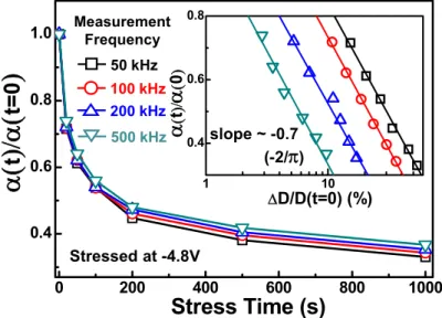
The time dependence of α(t) normalized to its initial value α(t=0) under CVSs from −4.6 to −5 V is plotted in Fig. 5. It was found that [α(t)/α(t=0)] decreases with increasing stress time for a given stress bias. In other words, CVS improves the voltage linearity of the high-κ La2O3 MIM
capacitor. This may be explained by the reduced carrier mobility in the La2O3 dielectric due to the
generation of stress-induced trap states under CVS, thus leading to a longer relaxation time of mobile charges. As mentioned before, α is dominated by the free carrier polarization. The inset of Fig. 5 shows the dependence of [α(t)/α(t=0)] on the relative variation in dielectric loss [ΔD/D(t=0)] during stress. The relative variation in dielectric loss caused by CVS with respect to its initial values is acquired as
(
)
0( )
0(
0(
)
)
0 0 0 − = Δ = = = D t D t D D t D t , (4)where D0(t=0) is the initial dielectric loss at zero bias. The relative variation in D of the La2O3
MIM capacitor under CVS increases with stress time and voltage (not shown), similar to the trend of the relative variation in capacitance shown in Fig. 3. It is believed that the trap/detrap processes are responsible for the dielectric loss, and the increase in D under CVS is ascribed to the generation of stress-induced trap states. Furthermore, from the inset of Fig. 5, [α(t)/α(t=0)] linearly decreases with a logarithmic increase in relative dielectric loss, and it maintains almost
6
the same slope independent of the stress voltage. This linear relationship further verifies the relationship between the amount of trap generation, responsible for the dielectric loss, and the reduction of free carrier mobility, responsible for the voltage dependence of capacitance. In other words, stress-induced trap states reduce the free carrier mobility in the dielectric and therefore increase the free carrier relaxation time that decreases the α of MIM capacitors under CVS. Additionally, the time dependence of [α(t)/α(t=0)] at various measurement frequencies under a CVS of −4.8 V is shown in Fig. 6, and the inset presents the dependence of [α(t)/α(t=0)] on the relative variation in dielectric loss [ΔD/D(t=0)]. As the measurement frequency increases, the changes in [α(t)/α(t=0)] become smaller. This is believed to be due to the smaller α(t=0) at higher frequency. From the inset of Fig. 6, [α(t)/α(t=0)] linearly decreases with a logarithmic increase in relative dielectric loss, and the slope is again independent of the measurement frequencies, and the same as that obtained in Fig. 5. As a result, one can derive that changes in κ must vary linearly with changes in D as well.
Figure 7 exhibits the cumulative results of The time-zero dielectric breakdown (TZDB) for the 10-nm La2O3 MIM capacitors at the measurement temperature varied from 25 to 125°C in the
case of top injection, the breakdown field (EBD) of 50% failure probability declines from 7.35 to
5.66 MV/cm as the temperature rises from 25 to 125°C. Besides, from the Fig. 7, it can be noted that as the measurement temperature raises, the distribution of the EBD data becomes narrower.
This temperature dependence of TZDB is related to the damage created in the oxide during the measurement. When carrying out the measurement, a rapid increase in applied voltage results in a rapid rise in local current density of the dielectric to generate energetic carriers that could release the energy and distort or weaken the local molecular bonds of the dielectric film. The weakened molecular bonds become very susceptible to be broken by the further injection carriers, and then a localized defective (percolation) site forms. As a conductive percolation path develops shorting the two electrodes, the breakdown occurs. For the high temperature measurement, more energetic injection carriers are available to create damage leading to lower breakdown voltage than that of low temperature measurement. The effective defect forming process at elevated temperature not only reduces the EBD magnitude, but also causes the dielectrics of different MIM capacitors break
down at almost the same applied voltage.
-2 -1 0 1 2 10.0 10.4 10.8 11.2 11.6 Cap aci tan ce Densit y
(
fF/ μ m 2)
Applied Voltage (V) -6 -4 -2 0 2 4 6 10-9 10-8 10-7 10-6 10-5 Cu rrent Density ( A/cm 2 ) Applied Voltage (V) Ni/10-nm La2O3 /TaN at 25oC 10 kHz 100 kHz Measurement Frequency Top Injection Bottom Injection α=775 ppm/V2 α=671 ppm/V2 Applied Voltage on Ni Electrode7
Fig. 2 The C-V curve, J-V curve, and the quadratic voltage coefficient (α) of a typical 10-nm La2O3 MIM capacitor. 0 200 400 600 800 1000 0.0 0.5 1.0 1.5 2.0 2.5 Δ C/ C(t=0) (%) Stress Time (s) 10-5 10-4 10-3 0.0 0.5 1.0 1.5 2.0 2.5 Δ C/C (t= 0) (%) Qinj(C/cm2 ) Ni/10-nm La2O3 /TaN -5 V -4.8 V -4.6 V Stress Bias at 100 kHz Y = 6.3 + 1.15 × log X
Fig. 3 Relative-capacitance variation [C0(t)-C0(0)]/C0(0) as a function of stress time and
injection charges (Qinj) at various CVS voltages from −4.6 V to −5 V.
0 -1 -2 -3 -4 -5 0 1 2 3 4 5 6 Δ C/ C(t = 0) (%) Stress Bias (V) 102 103 104 105 106 107 108 109 0 1 2 3 4 5 6 7 8 Δ C/ C( t= 0) (%) Stress Time (s) 10 year -4.6 V -4.4 V -4.2 V
Stress Bias 10-year Degradation 6.32%
4.09% 2.61%
-3.93 V
Fig. 4 The 10-year stability extraction of 10-nm La2O3 MIM capacitors estimated by the
relative-capacitance variation. 0 200 400 600 800 1000 0.4 0.6 0.8 1.0
Stress Time (s)
α(
t
)/α
(
t=0
)
10 20 30 40 50 0.4 0.6 0.8 α ( t )/ α ( t= 0 ) ΔD/D(t=0) (%) slope ~ -0.7 (-2/π) -5 V -4.8 V -4.6 V Stress Bias8
Fig. 5 Time dependence of the relative quadratic voltage coefficient of capacitance α(t)/α(0) under a CVS of −4.6 V to −5 V. 0 200 400 600 800 1000 0.4 0.6 0.8 1.0
α
(
t
)/
α
(
t=0
)
Stress Time (s)
1 10 0.4 0.6 0.8 ΔD/D(t=0) (%) α ( t )/ α ( 0 ) Stressed at -4.8V 50 kHz 100 kHz 200 kHz Measurement Frequency 500 kHz slope ~ -0.7 (-2/π)Fig. 6 Time dependence of the relative quadratic voltage coefficient of capacitance α(t)/α(0) under a CVS voltage of −4.8 V with various measurement frequencies.
5.5 6.0 6.5 7.0 7.5 0 20 40 60 80 100 Cumulative Pr obability (% )
Breakdown Electric Field (MV/cm)
25°C
50°C
75°C
100°C
125°C
Fig. 7 The cumulative results of TZDB for the 10-nm La2O3 MIM capacitors at the
measurement temperature varied from 25 °C to 125 °C.
四、結論
In this study, the MIM test structure with the high-k La2O3 film was fabricated and
characterized. The operational principles and the implementation issues of the high-k La2O3
MIM capacitor are discussed, including leakage current and conduction mechanisms, analog properties and distortion mechanisms, stress behaviors and degradation processes, as well as dielectric breakdown and reliability characteristics. In summary, a highly stable and reliable 10-nm La2O3 MIM capacitor with low leakage current (9.4 nA/cm2 at −1 V), high breakdown
strength (> 7 MV/cm at 25 °C), small VCC (671 ppm/V2 at 100 kHz), and sufficient high
capacitance density (11.4 fF/μm2) has been successfully demonstrated. The results highlight
9
五、參考文獻
[1] S. Y. Wu, “A new ferroelectric memory device, metal-ferroelectric-semiconductor transistor,” IEEE Trans. Electron Devices, vol. 21, no. 8, pp. 499-504, Aug. 1974.
[2] S. L. Miller and P. J. McWhorter, “Physics of the ferroelectric nonvolatile memory field effect transistor,” J. Appl. Phys., vol. 72, no. 12, pp.5999-6010, Dec. 1992.
[3] H. Buhay, S. Sinharoy, W. H. Kasner, and M. H. Francombe, “Pulsed laser deposition and ferroelectric characterization of bismuth titanate films,” Appl. Phys. Lett., vol. 58, no. 14, pp. 1470-1472, Apr. 1991.
[4] B.-C. Lan, C.-Y. Huang, and S.-Y. Chen, “Physical characteristics and electrical properties of Sr0.8Bi2-xTa2O9 films on Al2O3 Si annealed at high temperature,” J. Appl. Phys., vol. 94, no. 10, pp. 6735-6740, 2003.
[5] Y. Nakao, T. Nakamura, A. Kamisawa, and H. Takasu, “Study on ferroelectric thin films for application to NDRO nonvolatile memories,” Integr. Ferroelect., vol. 6, pp. 23-34, 1995. [6] N. A. Basit, H. K. Kim, and J. Blachere, “Growth of highly oriented Pb(Zr, Ti)O3 films on
MgO-buffered oxidized Si substrates and its application to ferroelectric nonvolatile memory field-effect transistors,” Appl. Phys. Lett., vol. 73, no. 26, pp. 3941-3943, Oct. 1998.
[7] T.-P. Ma and J.-P. Han,“Why is nonvolatile ferroelectric memory field-effect transistor still elusive,” IEEE Electron Device Lett., vol. 23, pp. 386-388, July 2002.
[8] C. T. Black, C. Farrell, and T. J. Licata, “Suppression of ferroelectric polarization by an adjustable depolarization field,” Appl. Phys. Lett., vol. 71, pp. 2041-2043, 1997.
[9] M. Takahashi, H. Sugiyama, T. Nakaiso, K. kodama, M. Noda, and M. Okuyama, “Analysis and improvement of retention time of memorized state of metal-ferroelectric-insulator-semiconductor structure for ferroelectric gate FET memory,”
Jpn. J. Appl. Phys. B, vol. 40, no. 4, pp. 2923-2927, Apr. 2001.
[10] E. Tokumitsu, R. Nakamura, and H. Ishiwara, “Nonvolatile memory operations of metal-ferroelectric-insulator-semiconductor (MFIS) FET’s using PLZT/STO/Si(100) structure,” IEEE Electron Device Lett., vol. 18, pp. 160-162, Apr. 1997.
[11] P.-C. Juan, C.-Y. Chang, and Y.-M. Lee, “A new metal-ferroelectric (PbZr0.53Ti0.47O3)-insulator (Dy2O3)-semiconductor (MFIS) for nonvolatile memory application,” IEEE Electron Device Lett., vol. 27, pp. 217-219, Apr. 2006.
[12] Y.-D. Su, W.-C. Shin, and Y.-M. Lee, “The effect of band offset on the retention properties of metal-ferroelectric (PbZr0.53Ti0.47O3)-insulator (Dy2O3, Y2O3)-semiconductor capacitors and field effect transistors,” Appl. Phys. Lett., vol. 91, pp. 122902-1-122902-3, Sept. 2007.
[13] H. Iwai, S. Ohmi, S. Akama, C. Ohshima, and A. Kikuchi, “Advanced gate dielectric materials for sub-100 nm CMOS,” in IEDM Tech. Dig., 2002, pp. 625–628.
[14] A. Chin, Y. H. Wu, S. B. Chen, C. C. Liao, and W. J. Chen, “High quality La2O3 and A12O3
gate dielectrics with equivalent oxide thickness 5-10 Å,” in Symp. VLSI Tech. Dig., 2000, pp. 16–17.
10
metallorganic chemical vapor deposition,” J. Electrochem. Soc., vol. 149, issue 6, pp. C345–C348, Apr. 2002.
[16] Y. H. Wu, M. Y. Yang, A. Chin, W. J. Chen, and C. M. Kwei, “Electrical characteristics of high quality La2O3 gate dielectric with equivalent oxide thickness of 5 Å,” IEEE Electron
Device Lett., vol.21, no. 7, pp. 341–343, July 2000.
[17] S. M. Sze, Physics of Semiconductor Devices, 2nd ed., Wiley, New York, 1981.
六、成果自評
此計畫經費支持一位博士班及一位碩士班學生執行研究及畢業。部分研究成果已整理成論 文,目前已發表或已被接受之論文共計有一篇國際期刊論文,兩篇國際研討會論文,論文 名稱與投稿期刊分別如下所示。且研究成果之論文撰寫與投稿仍在持續進行中。
七、發表國際期刊和國際會議論文
1. S.-H. Wu, C.-K. Deng, T.-H. Hou, and B.-S. Chiou, “Stability of La2O3
Metal-Insulator-Metal Capacitors Under Constant Voltage Stress,” accepted by Japanese
Journal of Applied Physics.
2. S.-H. Wu, C.-K. Deng, T.-H. Hou, and B.-S. Chiou, “Stability and Degradation Mechanism of La2O3 Metal-Insulator-Metal Capacitors Under Constant Voltage Stress,” to be presented
in the 217th Meeting of ECS, Vancouver, Canada, Apr. 25-30, 2010.
3. S.-H. Wu, C.-K. Deng, B.-S. Chiou, “Stabilities of La2O3 Metal-Insulator-Metal Capacitors
Under Constant Voltage Stress,” Proc. of the 2009 International Conference on Solid State
出席國際會議報告書
撰寫時間: 99 年 1 月 26 日 碩士生:吳杼樺 單位:交通大學電子研究所 E-mail: shwu.ee96g@nctu.edu.tw
本人有幸得到貴單位補助,參加位於日本東北之宮城縣仙台市舉辦的2009 年國際固態電子與材料會議(International Conference on Solid State Devices and Materials, SSDM 2009),會議自10月7日至10月9日共舉行三天,並帶回資料隨身 碟一份。這是此國際會議自1969年開始舉辦自今,首度提供參加者以USB隨身碟 儲存的所有會議相關資料及會議發表論文。不僅查閱迅速方便,而且可節省掉以 往提供紙本資料時的資源消耗,環保又有效率,獲得與會人士一致好評。由於 SSDM堪稱固態電子領域中歷史悠久且相當重要的學術會議,不但有來自世界各 地上千位的學術界、業界人士參加,系上也有許多教授及研究生共襄盛舉。
會議討論的主題共分十四個領域,包含Advanced Gate Stack / Si Processing and Material Science , CMOS Devices /Device Physics , Advanced Memory Technology,Applications of Nanotubes and Nanowires……等眾多現今固態電子中 備受矚目及極具潛力的技術。置身其中,不單是可以學習到許多新技術、新知識, 同時亦是與來自各地的科技研究人員交流的大好機會。而本人的論文“Stabilities of La2O3 Metal-Insulator-Metal Capacitors Under Constant Voltage Stress”,則發表於
Characterization and Materials Engineering for Interconnect Integration領域中RF Device/Process Technology的Oral Session。報告時間為15分鐘,另外還有5分鐘的 討論時間。由於現場聽眾提問討論踴躍,讓我獲益匪淺及得到許多靈感上的啟 發。系上的柯教授研究群也有發表一篇論文於同一領域,不過是發表在Poster Session裡。 最後,再次感謝行政院國家科學委員會補助經費讓本人成行,有機會出席這 麼重要的國際學術會議。不只學習、交流最新的技術與知識,為後續的研究奠定 良好基礎,更讓我充分體驗日本的整潔與辦事執行效率。希望往後台灣在學術研 究上能有更好的發展,在國際發光發亮!
Stabilities of La
2O
3Metal-Insulator-Metal Capacitors Under Constant Voltage Stress
Shu-Hua Wu, Chih-Kang Deng, and Bi-Shiou Chiou Institute of Electronics, National Chiao-Tung University, Taiwan
Phone: +886-3-5712121 ext: 54203; Fax: +886-3-5724361; E-mail: shwu.ee96g@nctu.edu.tw
1. Introduction
Recently, high-k metal-insulator-metal (MIM) capacitors integrated into backend interconnection as passive components have generated great interest for analog and RF applications [1], [2]. The stability of MIM capacitors is a key issue on precision performance, especially on the voltage linearity. Some studies [3], [4] have discussed the capacitance variation of SiO2 MIM capacitors during electrical stress. However, the
degradation of the MIM capacitor with high-k dielectric has not been well characterized. In this paper, the behaviors of La2O3 MIM capacitors under constant voltage stress (CVS)
were investigated. The correlations among the injected charges (Qinj), the capacitance change (ΔC/C0), the quadratic voltage
coefficient of capacitance (α), and the dielectric loss (D) of the La2O3 MIM capacitor were also discussed.
2. Device Fabrication and Experimental Procedures
This work focused on a 10-nm La2O3 MIM structure with
an 11.4-fF/µm2 capacitance density and an area of 2500 µm2. The schematic layout and the schematic cross section of the capacitor along the A-A’ line in the layout are shown in Figs. 1(a) and 1(b). The high-k dielectric La2O3 film was deposited
by e-beam evaporation and annealed in O2 ambient to improve
its quality. The top bi-layer (TaN/Ni) and bottom (TaN/Ta) electrodes were deposited by a reactive sputtering. All process temperatures during MIM capacitors fabrication were below 400 °C compatible with backend process. The samples were subjected to constant voltage stress in the range of −4.2 V to −5 V applied on the top electrode (Ni), and their capacitances variation were also measured at 25°C using an LCR meter at various intervals during CVS testing.
3. Results and Discussion
Fig. 2 shows C-V and J-V characteristics of the 10-nm La2O3 MIM capacitor. The leakage current is below 10-7 A/cm2
under the applied voltage of ±2 V. The quadratic voltage coefficient (α) of capacitance could be fitted by the second order polynomial equation: C (V) = C0 · (α · V2 + β · V + 1),
where C0 is the capacitance at zero bias. Hence, the values α
of 10-nm La2O3 MIM capacitor measured at 10 kHz and 100
kHz are 775 ppm/V2 and 671 ppm/V2, respectively.
Fig. 3 illustrates the correlations among the relative capacitance variation [C0(t)-C0(0)]/C0(0), the stress time, and
the injection charges (Qinj) at various CVS voltages from −4.6
V to −5 V, where C0(t=0) is an initial capacitance at zero bias.
As shown in the inset of Fig. 3, the relative-capacitance variation increases with a logarithmic increase in Qinj
regardless of the stress biases, which implies charge trapping in dielectric films [5]. When the carriers inject into the La2O3
dielectric film during CVS stress, the trapped charges could generate dipoles to increase the local permittivity and then contribute to the degradation of the capacitance [3], [4]. Besides, as shown in Fig. 3, after the [C0(t)-C0(0)]/C0(0)
rapidly increases in the initial stress, it tends to saturate after the 1000-s stressing. This saturation could be attributed to the trapped charges near the top electrodes. After the pre-existing trap states are rapidly filled by injection charges to increase the capacitance, the trapped charges would increase the barrier height near the injection electrode and result in a saturation phenomenon [6].
Fig. 4 depicts the 10-year stability extraction of a fabricated 10-nm La2O3 MIM capacitor estimated by the
relative-capacitance variation. It could be obtained from the extrapolated [C0(t)-C0(0)]/C0(0) versus stress time to 10 years,
as shown in the inset in Fig. 4. The 10-year degradations of 10-nm La2O3 MIM capacitors with an 11.4-fF/µm2 capacitance
are 6.32 %, 4.09 %, and 2.61 % under −4.6 V, −4.4 V, and −4.2 V, respectively. The safety 10-year operation voltage with below 1-% degradation could be extrapolated by around −4 V. This long-term stability is useful for the sub-65 nm technology node, whose operating voltage is smaller than 1.5 V.
Time dependence of α(t) normalized to its initial value α(0) under CVS biases from −4.6 V to −5 V is plotted in Fig. 5. The inset presents the dependence of α(t)/α(0) on the relative variation in dielectric loss [D0(t)-D0(0)]/D0(0) during stressing,
where D0(0) is the fresh dielectric loss at zero bias. It can be
found that α(t)/α(0) decreases with the increasing stress time for a certain stress bias. The reason for the decrease in the voltage dependence of capacitance is that the carrier mobility is reduced by the stress-induced trap states, and then hardly follows the alternating signal with a higher relaxation time [7]. Besides, α(t)/α(0) linearly decreases with a logarithmic increase in relative dielectric loss, but it still maintains almost the same slope under various stress voltages. It further verifies the change in voltage dispersion of capacitance is ascribed to the stress induced traps.
Dependence of α(t)/α(0) on stress time under a CVS of −4.8V with various measurement frequencies is exhibited in Fig. 6, and the inset presents the dependence of α(t)/α(0) on the relative variation in dielectric loss [D0(t)-D0(0)]/D0(0). As
the measurement frequency increases, the changes in α(t)/α(0) become smaller, and the correlation between α(t)/α(0) and the relative variation in D has been confirmed again.
4. Conclusions
The stabilities of MIM capacitors with La2O3 dielectric
under CVS are investigated in this paper. It could be found that the degradation in capacitance is dependent on injected charges (Qinj). The correlation between the carrier injection
and the relative-capacitance variation of La2O3 MIM
capacitors is also evaluated. The improvement in voltage nonlinearity of La2O3 MIM capacitors during CVS testing
could be attributed to the stress induced traps in dielectrics. Additionally, highly stability of 10-year lifetime was achieved for a 10-nm La2O3 MIM capacitor with an 11.4-fF/µm2
References
[1] C. Wenger et al., IEEE Trans. Electron Devices. 53 (2006) 1937.
[2] J. J. Yang et al., IEEE Electron Device Lett. 30 (2009) 460.
[3] C. Besset et al., Microelectron. Reliab. 43 (2003) 1237.
[4] C. C. Hung et al., IEEE Trans. Device and Reliab.7 (2007) 462.
[5] R. H. Walden et al., J. Appl. Phys. 43 (1972) 1178.
[6] R. Choi et al., IEEE Electron Device Lett. 26 (2005) 197.
[7] C. Zhu et al., IEDM Tech. Dig. (2003) 879.
Buffer Oxide Si Substrate
ILD1 TaN/Ni Top Electrode
ILD2 ILD2
ILD2
Al Al
TaN/Ta Bottom Electrode
10-nm La2O3
(b)
A’
A Cap.
(a)
Fig. 1. The schematic layout of the La2O3 MIM capacitor. (b) The schematic cross section of the capacitor along the A-A’ line in the layout shown in (a).
-2 -1 0 1 2 10.0 10.4 10.8 11.2 11.6 Capaciatnce Den s ity ( fF/ μ m 2 ) Applied Voltage (V) -6 -4 -2 0 2 4 6 10-9 10-8 10-7 10-6 10-5 Cur rent Densit y ( A/ cm 2 ) Applied Voltage (V)
Ni/10-nm La2O3 /TaN Meas. @ 25oC
10kHz 100kHz Measured Frequency Top Injection Bottom Injection α=775 ppm/V2 α=671 ppm/V2 Applied Voltage on Ni Electrode
Fig. 2. The C-V curve, J-V curve, and the quadratic voltage
coefficient (α) of a typical 10-nm La2O3 MIM capacitor.
0 200 400 600 800 1000 0.0 0.5 1.0 1.5 2.0 2.5 ( C 0 (t )-C 0 (0) ) /C 0 (0 ) ( % ) Stress Time (s) 10-5 10-4 10-3 0.0 0.5 1.0 1.5 2.0 2.5 ( C0 (t)-C0 (0 ) ) /C 0 (0 ) (%) Q inj(C/cm 2 ) Ni/10-nm La2O3 /TaN -5 V -4.8 V -4.6 V Stress Bias Meas. @ 100 kHz Y = 6.3 + 1.15 × log X
Fig. 3. Relative-capacitance variation [C0(t)-C0(0)]/C0(0) as a function of stress time and injection charges (Qinj) at various CVS voltages from −4.6 V to −5 V. 0 -1 -2 -3 -4 -5 0 1 2 3 4 5 6 ( C 0 (t )-C 0 (0 ) ) /C 0 (0 ) (% ) Stress Bias (V) 102 103 104 105 106 107 108 109 0 1 2 3 4 5 6 7 8 ( C0 (t)-C0 (0 ) ) /C 0 (0) (%) Stress Time (s) 10 yrs -4.6 V -4.4 V -4.2 V
Stress Bias 10-yrs Degradation
6.32 % 4.09 % 2.61 % -3.93 V 65-nm node below -1.5V
Fig. 4. The 10-year stability extraction of 10-nm La2O3 MIM capacitors estimated by the relative-capacitance variation.
0 200 400 600 800 1000 0.4 0.6 0.8 1.0 Stress Time (s)
α(
t)/α
(
0)
10 20 30 40 50 0.4 0.6 0.8 α ( t )/ α ( 0 ) (D 0(t)-D0(0))/D0(0) (%) slope ~ -0.7 -5 V -4.8 V -4.6 V Stress BiasFig. 5. Time dependence of the relative quadratic voltage coefficient
of capacitance α(t)/α(0) under a CVS of −4.6 V to −5 V. 0 200 400 600 800 1000 0.4 0.6 0.8 1.0
α
(
t)/
α
(
0)
Stress Time (s) 1 10 0.4 0.6 0.8 α ( t )/ α ( 0 ) (D 0(t)-D0(0))/D0(0) (%) Stressed at -4.8V slope ~ -0.7 50kHz 100kHz 200kHz Measured Frequency 500kHzFig. 6. Time dependence of the relative quadratic voltage coefficient
of capacitance α(t)/α(0) under a CVS voltage of −4.8 V with various measurement frequencies.