國 立 交 通 大 學
電 子 工 程 學 系 電 子 研 究 所
碩 士 論 文
背向散射理論應用於金氧半場效電晶體在飽和區之不
背向散射理論應用於金氧半場效電晶體在飽和區之不
背向散射理論應用於金氧半場效電晶體在飽和區之不
背向散射理論應用於金氧半場效電晶體在飽和區之不
匹配效應之物理模型
匹配效應之物理模型
匹配效應之物理模型
匹配效應之物理模型
A Physical MOSFET Saturation Current Mismatch Model Based
on Backscattering Theory
研 究 生:蔡鐘賢 Chung-Hsien Tsai 指導教授:陳明哲 Prof. Ming-Jer Chen
背向散射理論應用於金氧半場效電晶體在飽和區之不
背向散射理論應用於金氧半場效電晶體在飽和區之不
背向散射理論應用於金氧半場效電晶體在飽和區之不
背向散射理論應用於金氧半場效電晶體在飽和區之不
匹配效應之物理模型
匹配效應之物理模型
匹配效應之物理模型
匹配效應之物理模型
A Physical MOSFET Saturation Current Mismatch Model Based
on Backscattering Theory
研 究 生:蔡鐘賢 Student : Chung-Hsien Tsai 指導教授:陳明哲 Advisor:Prof. Ming-Jer Chen
國 立 交 通 大 學
電子工程學系 電子研究所碩士班
碩 士 論 文
A Thesis
Submitted to Department of Electronics Engineering & Institute of Electronics
College of Electrical Engineering and Computer Science National Chiao Tung University
in Partial Fulfillment of the Requirements for the Degree of
Master of Science In
Electronic Engineering July 2006
Hsinchu, Taiwan, Republic of China 中華民國 九十五 年 七 月
背向散射理論應用於金氧半場效電晶體在飽和區
背向散射理論應用於金氧半場效電晶體在飽和區
背向散射理論應用於金氧半場效電晶體在飽和區
背向散射理論應用於金氧半場效電晶體在飽和區不匹
不匹
不匹
不匹
配效應之物理模型
配效應之物理模型
配效應之物理模型
配效應之物理模型
研究生:蔡鐘賢 指導教授:陳明哲博士
國立交通大學
電子工程學系電子研究所
摘
摘
摘
摘
要
要
要
要
本論文研究金氧半場效電晶體在過臨界區的不匹配效應以及利 用背向散射理論推導出一個物理模型。我們首先量測各種不同尺寸的 電晶體,並且在飽和區計算其匹配誤差。我們發現隨著閘極電壓的增 大,電流的誤差會逐漸變小。接著我們考慮背向散射理論的三個參 數,背向散射係數, 臨界電壓, 以及汲極電壓導致位障下降, 組成一 個以這三個參數為變數的函數來計算電流的不匹配效應。A MOSFET Saturation Current Mismatch Model Based
on Backscattering Theory
Student:Chung-Hsien Tsai Advisor:Prof. Ming-Jer Chen
Department of Electronics Engineering Institute of Electronics
National Chiao Tung University
Abstract
This thesis investigates the current mismatch in above-threshold regions and derives a physical mismatch model based on backscattering theory. We have extensively characterized measured MOSFETs in above-threshold regions with different gate widths and lengths to determine the current mismatch. We have observed that the current mismatch decreases with increasing gate voltage. We have also derived a backscattering based mismatch model with three key parameters, drain-induce-barrier-lowering (DIBL), quasi-equilibrium threshold voltage Vtho, and backscattering coefficient rC. We can calculate the
current mismatch in above-threshold regions by using the new mismatch model.
Acknowledgement
做研究的生活是困難中帶點有趣,枯燥中帶點挑戰。如果沒有實 驗室的學長、同學、學弟,那麼研究生生活將會枯燥許多。感謝顏士 貴同學總是在我們有所鬆懈時的激勵,李建志同學在我們遇到瓶頸的 時候帶給我們的輕鬆,曾貴鴻同學在夜深人靜的時候跟我一起在實驗 室做實驗以及帶給實驗室的歡樂。感謝謝振宇學長無私的教導,呂明 霈學長的指導與扮演實驗室楷模的腳色。感謝李韋漢學弟的支援,許 智育學弟的幫忙。其中最感謝的就是陳明哲老師,教導我做研究應該 有的嚴謹態度以及研究方向上的指導,使得我的研究生生涯獲益良 多。最後感謝每一個在這兩年來幫助過我的人。Contents
Abstract (Chinese) ... i
Abstract (English) ...ii
Acknowledgement ...iii
Contents ...iii
Figure Captions... v
Chapter 1 Introduction
... 1Chapter 2 Backscattering Theory and Parameter Extraction
4 2.1 Backscattering Theory... 42.2 Parameter Extraction ... 6
Chapter 3 Mismatch Statistical Model
... 113.1 Mismatch in the above threshold region ... 11
3.2 Experiment... 11
3.3Analysis and Modeling... 12
Chapter 4 Conclusion
... 18Figure Captions
Fig.1 (a) Schematic illustration of channel backscattering theory in terms of cross section, and the conduction-band profile. F+, the incident flux from the source, is located at the peak of the source-channel barrier. F- is the incident flux from the drain. (b) A flux model in the saturation condition.
Fig.2 A schematic flowchart for the procedure of extracting r . c
Fig.3 Square symbol is measured C-V data at temperature of 298K. The dash line is from Schrödinger-Poisson simulation and the solid line is from the Berkeley’s C-V simulation.
Fig.4 Simulated inversion-layer charge density versus gate voltage under T=298K.
Fig.5 Simulated thermal injection velocity density versus gate voltage under T=298K.
Fig.6 Schematic illustration of determining Ceff from Qinv-V plot. G
Fig.7 Measured drain current versus gate voltage with T=298K for Lmask =90nm.
Fig.8 Schematic illustration of extracting Vthoby maximum g method from drain m
Fig.9 Threshold voltage at VD =0.025V versus Lmask with temperature as parameter.
Fig.10 Schematic constant current method of extracting ∆Vthfor DIBL.
Fig.11 Measured threshold voltage versus drain voltage.
Fig.12 Extracted threshold voltage versus L for VD = 1.0 V.
Fig.13 Extracted backscattering coefficient, r , versus gate voltage for (a) Vc D = 1.0
V, (b) VD = 0.5 V, and (c) VD = 0.1 V.
Fig.14 The used dies on wafer. All dies on wafer contain many n-channel MOS
transistors with the same structure
Fig.15 The drain current measured from different dies on wafer versus gate voltage
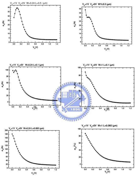
Fig.16 The coefficient of variance of the drain current versus gate voltage for
W/L=1um/0.5um, 1um/0.1um, 1um/0.065um, 0.24um/0.5um, 0.24um/0.1um,
0.24um/0.065um.
Fig.17 The measured drain current mismatch versus gate voltage for
W/L=0.24um/0.1um, and the fitting curve from Eq. (3.2) are shown for
comparison.
Fig.18 The measured drain current mismatch versus gate voltage for
0.24um/0.065um, and the fitting curves from Eq. (3.9) are shown for
comparison.
Fig.19 The coefficient of variance of the threshold voltage under the thermal
equilibrium condition Vtho versus the inverse square root of gate area.
Fig.20 The coefficient of variance of the drain-induce-barrier-lowering DIBL versus
the inverse square root of gate area.
Fig.21 The coefficient of variance of the backscattering coefficient rC versus the
inverse gate length.
Fig.22 The experimentally extracted σVtho versus the inverse square root of gate
area and the proportionality constants AVtho.
Fig.23 The experimentally extracted σDIBL versus the inverse square root of gate
area and the proportionality constants ADIBL.
Fig.24 The experimentally extracted σrc versus the inverse gate length and the
proportionality constants Arc.
Fig.25 The measured drain current mismatch versus gate voltage for
W/L=1µm/0.5µm, 1µm/0.1µm, and 1µm/0.065µm; 0.24µm/0.5µm, 0.24µm/0.1µm, and 0.24µm/0.065µm. The calculated results from Eq. (3.11) are also shown for comparison.
Chapter 1
Introduction
It is well recognized that no two things in the world are exactly the same. This is why everything comes with tolerance. The same situation can be applied to MOSFET: no two transistors can be the same even they are identically drawn. For example, threshold voltages are different, drain currents are different, etc. Mismatch reflects the different performance of two or more devices under the same operation. It is widely recognized that mismatch is a key to precision analog IC design. If not properly controlled, mismatch results in the performance degradation, the circuit malfunction, and even the drop of yield. Thus as device becomes smaller in today’s VLSI technology, mismatch analysis becomes more and more important.
Mismatch in above threshold region
Because most of the transistors in the circuit operate under the saturation region, the mismatch in the saturation region is noticed. From the traditional drain current model:
2 ( ) OX GS th W ID C V V L µ = −
We derive the current mismatch formula by using the drain current model based on backscattering model to resplace the traditional drain current model.
Mismatch model
Although many mismatch models based on process parameters have been reported, the physical mismatch model using backscattering theory has never been discussed. As stated in backscattering theory, the nanoscale device performance is ultimately limited by the injection velocity and backscattering coefficient. The concept of channel backscattering is shown in Fig. 1. Both the carrier injection velocity and backscattering coefficient determine the current drive in nanoscale devices in the saturation region as given by [1,2]
,
1
[ ( )]
1
c
D sat eff inj G tho D
c r I WC v V V DIBL V r − = − − × +
where vinj, rc, and Vtho are the thermal injection velocity at the top of
source-channel junction barrier, the channel backscattering coefficient through the kBT layer,and the near thermal equilibrium threshold voltage,
in saturation region based on backscattering theory that has successfully reproduced the mismatch data in strong inversion for different dimensions. With this model included, the current mismatch can be expressed as a function of the coefficient of variation in the parameters : Vtho, rc, and DIBL.
Chapter 2
Backscattering Theory and Parameter Extraction
In this section, we will explain the backscattering theory and the method of extracting the parameters. The main extraction procedure is demonstrated on the device size of W=1um and L= 0.1µm with the measurement conditions: VG= 0~1.2V; VD= 0.01, 0.1, 0.5, and 1.0V; and
the operating temperature = 298。K
Section 2.1 Backscattering Theory
The channel backscattering theory describes a wave-like transport of carriers through the channel from the source to drain. As schematically shown in Fig 1, the channel is separated into two parts : 0<x<l and
l<x<Leff. Here l represents the critical length from the source the
conduction band bends down by a thermal energy of kBT, where kB is
Boltzmann’s constant , L is the channel length and T is the temperature. Within the kBT layer, multiple backscattering process occurs [2], [3]. In
the channel, scattering occurs due to the presence of impurity atoms, lattice vibration of the atoms, and surface roughness. A certain fraction rC
The total charge in the inversion layer comprises the injected and reflected components, is controlled by MOS electrostatics. The transmitted flux (1- rC)F out of the kBT layer undergoes no net reflections
to kBT layer due to significant potential gradient in the remainder of
channel. Consequently, the drain current per unit channel width can be expressed as D
1
I
1
C i n v i n j Cr
Q
v
r
−
=
+
(1)
Where Qinv is the inversion-layer charge density per unit area and vinj is
the thermal injection velocity.
Experimentally, rC can be extracted by current-voltage (I-V) fitting
[3]-[5]. Owing to multiple backscatterings in the kBT layer, both the
quasi-equilibrium mean-free-path λ and the width of kBT layer are
functionally coupled through a single rC [2]
1
(2)
1
Cr
l
λ
=
+
In the saturation region, the formula of drain current region based on backscattering theory can be described as
(3)
1
(
)
1
c Dsat eff G th inj
c
r
I
WC
V
V v
r
−
=
−
+
In real devices, the terminal drain current involves the drain / source series resistances, RD and RS , and
(Drain-Induced-Barrier-Lowering) DIBL. Thus the expression (3) is augmented into c c inj D D S D D tho S D G eff Dsat r r v R I R I V DIBL V R I V WC I + − − − × − − − = 1 1 ))] ( ( ) [( (4)
Here we neglect RS and RD, the formula can be expressed as
1
[( ( )]
1
c
Dsat eff G tho D inj
c r I WC V V DIBL V v r − = − − × + (5)
Section 2.2 Parameter Extraction
Flow-chart
Fig. 2 summarizes schematically the procedure of extracting rC . The
connection lines illustrate the relationship between the data and how to derive them in series. We would then demonstrate the extraction procedure based on the connection lines of the flow-chart.
C-V Fitting
The measured C-V curve is compared with the calculated one by the quantum simulator with the gate oxide thickness TOX, poly doping
concentration Npoly and channel doping concentration Nsub as input.
TOX , Npoly and Nsub each can be adjusted to affect the C-V curve, but only
match. As shown in Fig. 3 TOX , Npoly and Nsub are simultaneously
obtained by C-V fitting. Here, two different C-V comparisons were done: one from Schrodinger-Poisson solving [6] and the other from Berkeley’s C-V simulation. They can both create desirable results, besides at high voltage where leakage current occurred in real experiment. C-V fitting eventually led to TOX = 1.4 nm, Npoly = 2.5×10
20
cm-3, and Nsub = 6×10 17
cm-3 .
Quasi-Equilibrium Device Parameter
With known TOX , Npoly and Nsub as input, the Schrodinger-Poisson
solver was carried out to calculate the inversion layer Qinv, the thermal
injection velocity vinj, and the effective gate capacitance Ceff. Fig. 4 shows
the calculated inversion charges, Qinv , versus gate voltage. The thermal
velocity, vinj , is displayed in Fig. 5 versus gate voltage. From these results,
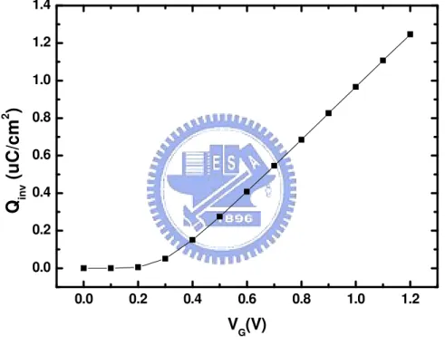
some properties can be drawn. First, at low gate voltage, or at the non-degenerate limit, the thermal velocity is regardless of gate voltage. Second, at the high gate voltage, or near degenerate limit, the thermal velocity increases with gate voltage. According to MOS electrostatics, Qinv can be expressed as
)
(
G tho eff s invqn
C
V
V
Q
=
=
−
(6) The effective oxide capacitive Ceff is defined by [7]Q I Q I eff C C C C C + = (7)
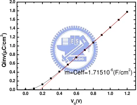
whereCIis the gate dielectric capacitance and CQis the semiconductor
(or quantum) capacitance related to the quantum mechanical confinement, polysilicon depletion, finite density-of-states, etc. From the slope of the
inv
Q versusVGS, as shown in Fig. 6,we obtain Ceff = 1.3926×10⁻⁶(F/cm2).
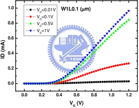
Drain Current against Gate Voltage
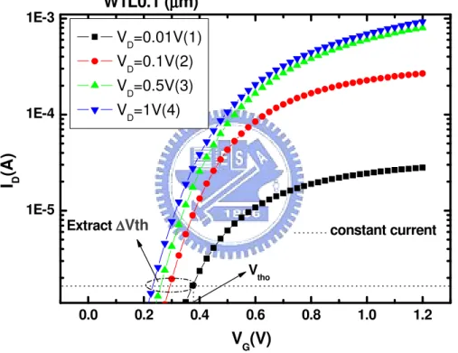
The drain current versus gate voltage, ID−VG, is measured under
temperatures = 298K for different drain voltages of 0.01V, 0.1V, 0.5V, and 1.0V. The results are shown in Fig. 7 for W=1um, and L=0.1um.
Threshold Voltage
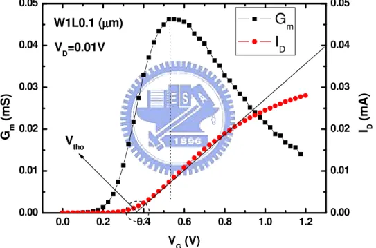
The threshold voltage is a key parameter in MOSFET design and modeling. There are many definitions and extraction methods for the threshold voltage. In this work, we employ a maximum trans-conductance method in the linear region to assess quasi-equilibrium threshold voltage and the constant subthreshold current method in the
saturation region to extract the DIBL [8].
Quasi-Equilibrium Threshold Voltage Extraction
The maximum-gm method is used in the linear region with a lowVDSof
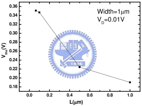
10mV. In this method, a tangent line is established at the drain current with the maximum trans-conductance, as shown in Fig. 8. Through linear extrapolation to zero drain current, the quasi- equilibrium threshold voltage Vthowas obtained. Fig. 9 shows the extracted Vthoversus L. For L
of 0.1um, Vtho= 0.34688V for temperature of 298
。
k.
DIBL Extraction
With channel length scaling down, it is gradually important to consider short-channel effects such as Vth roll-off and Drain Induced
Barrier-Lowering (DIBL). We use constant subthreshold current method to determine threshold voltage operating in the saturation region (high VDS). The critical constant current is defined as the drain current when the
gate voltage is the threshold voltage from the maximum-gm method in the linear region [8], as shown in Fig. 10.
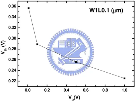
Drain-induced-barrier-lowering (DIBL) is defined as the gate voltage shift (∆VGS) at the constant drain current due to a change in the drain voltage(∆VDS). From Fig. 11, threshold voltage reduction due to
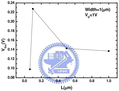
increasing VDS is mainly due to the DIBL effect. Fig. 12 shows threshold
voltage versus L for drain voltage of 1 V. It can be seen that DIBL effect is insignificant for the long-channel device. With the channel shortening, DIBL effect imposes increasing influence on the threshold voltage.
Results
According to the drain current formula (5), we can see that the parameters, Ceff , vinj , DIBL, Vth , and rC , have been extracted. Thus, the
backscattering coefficient rC can be extracted by I-V fitting. The results
are given in Fig. 13 (a) against gate voltage for VD= 1V. Fig. 20 (b) and
(c) are the case of VD= 0.5V and 0.1V, respectively. From Fig. 13, it can
be seen that (1) rC decreases with increasing gate voltage and then,
critically, tends to saturate for VG≥0.8V; and (2) at VD=0.1V, rC is nearly
Chapter 3
Mismatch Statistical Model
Section 3.1 Mismatch in the above threshold region
We have extensively measured and analyzed the current mismatch of a small-size n-channel MOS transistor operated in the above threshold region with its p-well-to-n+ source junction forward and reverse biased. The measured dependencies of the mismatch in the saturation region have been successfully reproduced by a new simple statistical model based on backscattering theory.
The transistors in the circuit usually operate in the saturation region, and one of the fundamental factors limiting the accuracy of MOS circuits operated in the saturation region is the current mismatch between identically designed devices. The poor control over the current match can cause a number of undesirable effects in the circuit level. Especially, in nanoscale devices, the effects are more and more serious.
Section 3.2 Experiment
achieved in terms of the dies on wafer as schematically shown in Fig. 14. All dies on wafer containing many n-channel MOS transistors have the same structure. They were fabricated using a 65 nm CMOS process. In our measurement of current mismatch, the p-well-to-n+-source bias, VBS,
was fixed when sweeping VGS from 0 to 1.2 V in a step of 25 mV. The
drain currents were measured and recorded for the subsequent analysis. The measurement setup contained the HP4156B and a Faraday box for shielding the test wafer, all performed in an air-conditioned room with the temperature fixed at 298。K. The total measurement time of one die’s n-channel MOS for these full ranges was about 3 hours. A total of 25 n-channel MOS FETs were measured in one die. Fig. 15 depicts a typical measured I-V characteristic with VGS and VDS as parameters for the
shown device size of W=0.24(um), and L=0.1(um).
Section 3.3
Analysis and Modeling
The drain current mismatch σID is defined as the coefficient of variance
of ID: σID = ID (SD)/ID (mean) where ID (mean) and ID (SD) are the mean and SD
( standard deviation ) of drain current for all the same dimensions of n-channel MOS FETs. We analyze six device sizes from the data by
experiment, and calculate the mean and SD by a statistical tool. Fig. 16 shows the diagram of the calculated σID for different VGS. From Fig. 16
we can observe that the drain current mismatch decreases with the increasing of VGS and becomes flat in above threshold region. From the
backscattering theory, the drain current in the saturation region can be expressed as
1
[( ( )]
1
c
Dsat eff G tho D inj
c r I WC V V DIBL V v r − = − − × + (3.1)
Now we propose a new simple statistical model to quantitatively account for the above observed dependencies of the mismatch in the above threshold region on the gate-to-source bias. As revealed by (3.1), our observed mismatch as a function of the VGS can be attributed to the
coefficient of variation in the threshold voltage under the thermal equilibrium condition VTHO, the drain-induce-barrier-lowering DIBL, and
the channel backscattering coefficient rC. From (3.1) the mismatch of the
current , σID, can be derived as a function of the three coefficients of
variance of the parameters : the coefficient of variance of the threshold voltage, σVtho, the coefficient of variance of the
channel backscattering coefficient σrc : ( ) ( ) ( )
(
)
( ) ( ) × σ = σ + − − × σ + σ − − × − 2 2 2 DIBL 2 2 2 2 2 2 2 2 [ ( )] 4 [ ( )] 1 D ID G tho D c tho rc Vtho G tho D c DIBL V V V DIBL V r V V V DIBL V r (3.2)This new formulation explicitly describes the dependence of σID on VGS.
We can extract the VTHO , DIBL, and rC from the drain currents of all dies
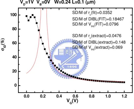
on wafer that we measured, and calculate the coefficient of variance of the σVtho, σDIBL, and σrc. We calculate the σrc under VG=1V and VB=0V
because the change of σrc with gate voltage is very small. Fig. 17 shows
that we use the backscattering mismatch model to reproduce the curve of the coefficient of variance of drain current versus VGS (VGS >0.5V) at
VD=1V, VB=0V by calculating the appropriate σVtho, σDIBL, and σrc for the
device size of width=0.24um, and length=0.1um. Thus we compare the parameters calculated with the parameters extracted by experiment: it can be observed that the differences between the calculated calculated parameters and experimentally extracted parameters are small.
Mismatch model derivation based on backscattering theory
The variance or standard deviation σg(x,y,z) with three random variables of
2 2 2 2 2 2 2 ( , , ) ( ) ( ) ( ) 2( )( ) ( , ) 2( )( ) ( , ) 2( )( ) ( , ) g x y z x x z OV OV OV g g g g g C x y x y z x y g g g g C x z C y z x z z y σ ≅ ∂ σ + ∂ σ + ∂ σ + ∂ ∂ ∂ ∂ ∂ ∂ ∂ ∂ ∂ ∂ ∂ + + ∂ ∂ ∂ ∂ (3.3)
where σx, σy and σz are the variances of x, y and z, respectively; and
COV(x,y), COV(x,z) and COV(y,z) is the correlation coefficient between (x,
y), (x,z) and (y,z). To facilitate the analysis, we assume that COV(x,y),
COV(x,z) and COV(y,z) all are zero. Thus the coefficient of variance in the
drain current ID can be written as
( ) ( ) ( )
(
)
( ) ( ) × σ = σ + − − × σ + σ − − × − 2 2 2 2 2 2 2 2 2 2 2 [ ( )] 4 [ ( )] 1 D ID DIBL G tho D c tho rc Vtho G tho D c DIBL V V V DIBL V r V V V DIBL V r (3.4)The following backscattering current expression is considered for the mismatch model
1
[( ( )]
1
c
Dsat eff G tho D inj
c r I WC V V DIBL V v r − = − − × + (3.5) From (3.5) derivatives in (3.4) can easily be derived:
[ ] tho D tho D tho GS tho D V I V I V V V DIBL V − ∂ = ∂ − + • ; (3.6) [ ] D D D GS tho D I DIBL V DIBL I DIBL V V DIBL V ∂ • = ∂ − + • ; (3.7) and 2 2 [1 ] C D C D C C r I r I r r − ∂ = ∂ − (3.8)
Thus we obtain a compact model : ( ) ( )
(
)
( ) ( ) × σ = σ + σ + σ − − × − − − × 2 2 2 2 2 2 2 2 2 2 4 [ ( )] 1 [ ( )] D c tho ID DIBL rc Vtho G tho D c G tho D DIBL V r V V V DIBL V r V V DIBL V (3.9) Apparently, (3.9) analytically expresses the current mismatch in strong inversion as function of the parameters of backscattering theory. We use (3.9) to reproduce the curve of current mismatch in other five device sizes by calculating σVtho, σDIBL, σrc in Fig. 18 and compare the calculatedparameters with the experimentally extracted parameters. We can then observe that the differences between the two are small.
The corresponding calculated parameters and experimentally extracted parameters σVtho, and σDIBL versus the inverse square root of the device
area are plotted in Fig. 19, and Fig. 20. The σrc versus the channel length
are plotted in Fig. 21. From these figures we can observe that the coefficients of variance of Vtho and DIBL increase with decreasing device
area, and the coefficient of variance of rC increases with decreasing
channel length. From Fig. 22, Fig. 23, and Fig. 24, we have
Vtho DIBL rc Vtho DIBL rc
A
A
A
σ
=
, σ
=
, and σ =
L
WL
WL
(3.10) where AVtho, ADIBL, and Arc are the size proportionality constants for σVtho,σDIBL, and σDIBL respectively. The extracted values lead to AVtho
=0.01406µm, ADIBL =0.0296µm, and Arc =0.00702µm. Therefore, we use
(3.10) to substitute (3.9) ( )
(
)
2 2 2 2 2 2 rc Vtho DIBL 2 2 2 2 4 A A A [ ( )] WL 1 L [ ( )] WL D c tho ID G tho D c G tho D DIBL V r V V V DIBL V r V V DIBL V σ = × + + − − × − − − × (3.11) We can calculate the drain current mismatch in the saturation region from (3.11) and compare with the curves of experimentally extracted σID versusgate voltage for W/L=1µm/0.5µm, 1µm/0.1µm, and 1µm/0.065µm; 0.24µm/0.5µm, 0.24µm/0.1µm, and 0.24µm/0.065µm in Fig. 25, and we can observe that (3.11) can serve as a useful analytic tool for properly calculating the mismatch.
Chapter 4
Conclusion
Mismatch is an important issue in today’s VLSI technology. Lots of transistors in the circuit operate in the saturation region. We use the backscattering theory to derive the mismatch model in the saturation region. The drain current model in saturation based on backscattering theory is performed more accurately than the traditional drain current model in the nanoscale devices. We extract the parameters in a wide range of long channel to nanoscale channel MOSFETs and successfully use the new mismatch model to reproduce the experimental current mismatch.
References:
[1] M. S. Lundstrom, “Elementary scattering theory of the Si MOSFET,”
IEEE Electron Device Letters, vol. 18, pp. 361-363, July 1997.
[2] D.K. Ferry, R. Akis, D. Vasileska, “Quantum effects in MOSFETs: use of an effective potential in 3D Monte Carlo simulation of ultra-short channel devices,” IEDM Tech. Digest, pp. 287 -290, 2000.
[3] M. S. Lundstrom and Z. Ren, “Essential physics of carrier transport in nanoscale MOSFETs,” IEEE Trans. Electron Devices, vol. 49, pp. 133-141, Jan. 2002.
[4] M.-J. Chen, H.-T. Huang, K.-C. Huang, P.-N. Chen, C.-S. Chang, and C. H. Diaz, “Temperature dependent channel backscattering coefficients in nanoscale MOSFETs,” in IEDM Tech. Dig., Dec. 2002, pp. 39-42.
[5] G. Timp, J. Bude, K. K. Bourdelle, J. Garno, A. Ghetti, H. Gossmann, M. Green, G. Forsyth, Y. Kim, R. Kleiman, F. Klemens, A. Kornblit, C. Lochstampfor, W. Mansfield, S. Moccio, T. Sorsch, D. M. Tennant, W. Timp, and R. Tung, “The ballistic nano-transistor,” in
[6] http://www.nanohub.purdue.edu
[7] Jing Wang, and M. S. Lundstrom, “Ballistic transport in high electron mobility transistor,” IEEE Trans. Electron Devices, vol. 50, pp. 1404-1609, Sept. 2003.
[8] X. Zhou, K.Y. Lim, and D. Lim, “A simple and unambiguous definition of threshold voltage and its implications in deep-submicron MOS device modeling,” IEEE Trans. Electron
Fig. 1
VG(>Vth)
l
0
2DEG(2-Dimensional Electron Gas)
VD n+ n+ x kBT EC1 (VD= 0 V) EC2 (VD≠≠≠≠ 0 V) F+ F -T’F -TF+ x F rcF (1-rc)F 0 l
Source Channel Drain
(a)
(b)
Leff J-(0) J+(0) VG(>Vth) l 02DEG(2-Dimensional Electron Gas)
VD n+ n+ x kBT EC1 (VD= 0 V) EC2 (VD≠≠≠≠ 0 V) F+ F -T’F -TF+ x F rcF (1-rc)F 0 l
Source Channel Drain
(a)
(b)
Leff
-2.0 -1.5 -1.0 -0.5 0.0
0.5
1.0
1.5
0.0
0.4
0.8
1.2
1.6
2.0
2.4
Ca
p
a
c
it
a
n
c
e
(
µµµµ
F
/c
m
2)
V
bias(V)
Experiment
Schrodinger-Poisson Solving
Berkeley's C-V Simulation
Schrödinger-Poisson Simulation
-2.0 -1.5 -1.0 -0.5 0.0
0.5
1.0
1.5
0.0
0.4
0.8
1.2
1.6
2.0
2.4
Ca
p
a
c
it
a
n
c
e
(
µµµµ
F
/c
m
2)
V
bias(V)
Experiment
Schrodinger-Poisson Solving
Berkeley's C-V Simulation
Schrödinger-Poisson Simulation
Fig 3
Fig. 4
0.0 0.2 0.4 0.6 0.8 1.0 1.2 0.0 0.2 0.4 0.6 0.8 1.0 1.2 1.4 Q in v ( u C /c m 2 ) VG(V)\
Fig. 5
0.0 0.2 0.4 0.6 0.8 1.0 1.2 1.15 1.20 1.25 1.30 1.35 1.40 1.45 Vi n j(1 0 7 c m /s ) VG(V)Fig. 6
0.0 0.2 0.4 0.6 0.8 1.0 1.2 0.0 0.2 0.4 0.6 0.8 1.0 1.2 1.4 1.6 1.8 2.0 Q in v (µµµµ C /c m 2 ) V G(V)m=Ceff=1.71510
-6(F/cm
2)
Fig. 7
0.0 0.2 0.4 0.6 0.8 1.0 1.2 0.0 0.2 0.4 0.6 0.8 1.0 ID (m A ) V G (V) VD=0.01V V D=0.1V VD=0.5V V D=1V W1L0.1 (µµµµm)Fig. 8
0.0 0.2 0.4 0.6 0.8 1.0 1.2 0.00 0.01 0.02 0.03 0.04 0.05 0.00 0.01 0.02 0.03 0.04 0.05 I D ( m A ) G m ( m S ) VG (V)G
mI
D Vtho W1L0.1 (µµµµm) VD=0.01VFig. 9
0.0 0.2 0.4 0.6 0.8 1.0 0.18 0.20 0.22 0.24 0.26 0.28 0.30 0.32 0.34 0.36 V th o (V ) L(µµµµm)Width=1
µm
V
D=0.01V
Fig. 10
0.0 0.2 0.4 0.6 0.8 1.0 1.2 1E-5 1E-4 1E-3 I D (A ) VG(V) V D=0.01V(1) V D=0.1V(2) V D=0.5V(3) V D=1V(4) W1L0.1 (µµµµm) Vtho constant current Extract ∆∆∆∆VthFig. 11
0.0 0.2 0.4 0.6 0.8 1.0 0.22 0.24 0.26 0.28 0.30 0.32 0.34 0.36 V th ( V ) VD(V) W1L0.1 (µµµµm)Fig. 12
0.0 0.2 0.4 0.6 0.8 1.0 0.08 0.10 0.12 0.14 0.16 0.18 0.20 0.22 0.24 V th o (V ) L(µµµµm) Width=1(µµµµm) VD=1V0.4 0.6 0.8 1.0 1.2 0.0 0.1 0.2 0.3 0.4 0.5 0.6 0.7 0.8 0.9 1.0 rC VG(V) VD=1V (a) 0.4 0.6 0.8 1.0 1.2 0.0 0.1 0.2 0.3 0.4 0.5 0.6 0.7 0.8 0.9 1.0 rC VG(V) V D=0.5V (b) 0.4 0.6 0.8 1.0 1.2 0.0 0.1 0.2 0.3 0.4 0.5 0.6 0.7 0.8 0.9 1.0 rC VG(V) VD=0.1V (c)
Fig. 13
0.0 0.2 0.4 0.6 0.8 1.0 1.2 0.00 0.05 0.10 0.15 0.20 0.25 1 2 3 4 5 6 7 8 9 1011121314 151617 1819 2021 2223 2425 2627 28 29 30 31 32 33 34 35 36 37 38 39 4041 42 4344 4546 4748 49 A B C D E F G H I J K LM NO P QRS TU VW XY ZAA AB ACAD AEAF AGAH AI AJAK AL AMAN AOAP AQAR ASAT AU AVAW a b c d e f g h i j k l mn o p qr st uv wx yz aaab ac adae af ag ahai ajak al aman aoap aqar as atau av aw I D ( m A ) V G(V) V D=1V VB=0V W0.24L0.1 (µµµµm)