Synthesis of two-dimensional photonic crystals
for large band gaps
Yi-Kuan Liao, Yean-Woei Kiang and C. C. Yang
Graduate Institute of Electro-Optical Engineering, Graduate Institute of Communication Engineering,
and Department of Electrical Engineering,
National Taiwan University,
No. 1, Sec. 4, Roosevelt Road, Taipei, Taiwan
Email: [email protected]
ABSTRACT
For a photonic crystal, the larger the photonic band gap (PBG), the greater the bandwidth for manipulating the optical wave propagation. Therefore, to enlarge the photonic band gaps would be an important research topic. In this paper, we adopt the simulated annealing (SA) algorithm to synthesize two-dimensional photonic crystals for large band gaps. The SA is an iterative procedure and its probabilistic nature provides an opportunity to escape from the local minima and to reach the global minimum in a nonlinear optimization problem. To speed up the numerical calculations, we also use the fast plane wave expansion method for calculating the band diagram of a photonic crystal at each iteration step of the SA procedure. Numerical simulations are carried out to demonstrate the feasibility and effectiveness of our synthesis algorithms.
Keywords: synthesis, photonic crystal, photonic band gap, simulated annealing.
1. INTRODUCTION
A photonic crystal is a periodic structure composed of two or more different dielectric materials. While the refractive index contrast is sufficiently high, certain frequency ranges in which electromagnetic waves are forbidden to propagate may appear.1-3 The electronic analogy is the valence and conduction energy bands in semiconductors. Due to
the Bragg-like diffraction from the atoms, certain energy bands are forbidden for electrons to propagate. If the lattice potential is strong enough, the gap of energy bands might extend to all possible directions, resulting in a complete band gap. In recent years, the study of photonic crystals has received much attention because of the capability of inhibiting the optical wave propagation in certain frequency ranges, known as the photonic band gaps (PBGs). With photonic crystals, one can manipulate the optical wave in a wavelength scale, leading to many applications such as waveguides, micro-cavities, filters, etc.
As mentioned previously, many applications of photonic crystals are based on the PBG. For a photonic crystal, the larger the PBG, the greater the bandwidth for inhibiting the wave propagation, and the more the flexibility for manipulating the optical wave. Therefore, to enlarge the PBG would be an important issue of research. Several numerical techniques have been proposed to treat the problem of enlarging the PBG.4-7 However, this synthesis problem is quite
challenging and there is still room for improvement.
Usually, it is difficult for a simple photonic crystal with periodic dielectric rods or air holes to have an absolute PBG. To synthesize a photonic crystal with an absolute PBG, one has to find the photonic crystal of particular pattern systemically. In this research, the simulated annealing (SA) algorithms8 together with the fast plane wave expansion
method4 are used to synthesize the photonic crystals for large PBGs. Numerical simulations are conducted to verify the
feasibility of our approach. For simplicity, we focus on the two-dimensional (2D) photonic crystals. This research would provide some essential insight to synthesize three-dimensional (3D) or more complicated photonic crystal structures. The concept and algorithms of the SA are described in section 2. Numerical results are discussed in section 3. Finally, some conclusions are drawn in section 4.
Optoelectronic Materials and Devices for Optical Communications, edited by Shinji Tsuji, Jens Buus, Yi Luo, Proc. of SPIE Vol. 6020,
602017, (2005) · 0277-786X/05/$15 · doi: 10.1117/12.635638 Proc. of SPIE Vol. 6020 602017-1
2. SIMULATED ANNEALING
The simulated annealing is an effective optimization algorithm used to solve nonlinear optimization problems. It is motivated by an analogy to annealing in solids. If one heats a solid to exceed the melting point and then cools it, the structural properties of this solid depend on the rate of cooling. If the liquid is cooled slowly enough, large crystals will be formed. However, if the liquid is cooled quickly (quenched), the crystals will contain imperfections. The SA technique was introduced by Kirkpatrick et al. in 1983 to optimize the wire routing on a printed circuit board,8 though the foundation
for this algorithm was given by Metropolis et al. in the 1950s.9 In the following, the algorithm of SA for finding photonic
crystals for large absolute band gaps will be described.
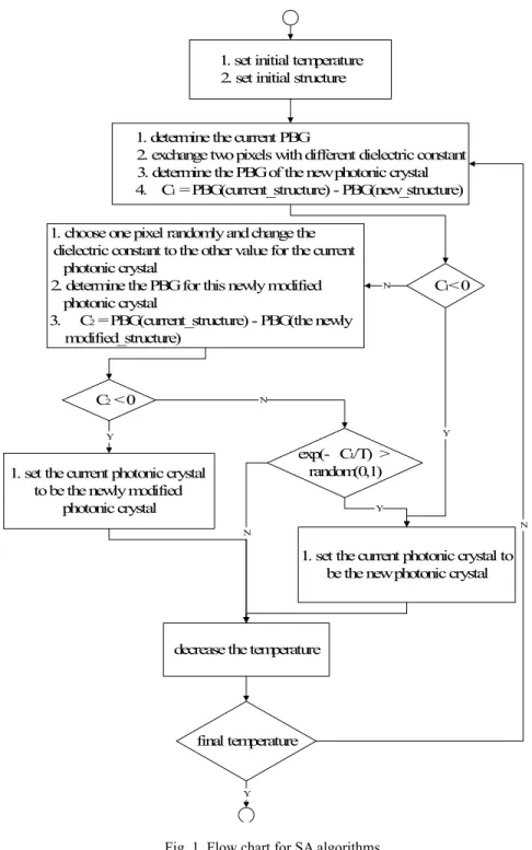
The SA is an iterative procedure that updates one candidate solution successively until a termination condition is satisfied. A candidate solution is randomly generated according to some probabilistic rule, and we define a cost function to evaluate the cost of the problem. The SA algorithm we used is described in a flow chart shown in Fig. 1. Here the temperature T is a virtual parameter that controls the iterative process, and ∆C1 is the change of the cost function which is
defined as the negative of PBG. The unit cell of the photonic crystal is divided into pixels, and each of these pixels could be one of two prescribed dielectric materials. At the beginning, we define the initial temperature and the initial structure of photonic crystal. Then we change the current photonic crystal by exchanging two different dielectric pixels randomly. If the value of absolute PBG of the new photonic crystal is larger than that of the current one, we accept the new photonic crystal structure and go to the next iteration. If, on the contrary, the new value of PBG is smaller than the current one, further manipulation is needed. We select one pixel of the current photonic crystal randomly and change its dielectric constant to the other value to check if the PBG of the newly modified structure is larger than that of the current photonic crystal. We accept the newly modified photonic crystal if now the value of PBG is indeed increased. However, if the new value of PBG is still smaller than the current one, we do not accept the modified photonic crystal structure unless the condition exp(−∆C T1/ )> random(0,1) is satisfied. Note that the SA algorithm provides an opportunity for us to escape from a local minimum and, finally, to reach the global minimum of the optimization problem. This is the basic and intriguing characteristic of the SA. Since the band diagram of the photonic crystal has to be calculated at each iteration step and a large number of iterations are usually needed, the SA process is quite time-consuming. To save computing time, we adopt a fast plane wave expansion method4 for calculating band diagram of photonic crystals. Based on this fast
algorithm, we are able to rapidly determine the value of photonic band gap at each iteration step, and then to improve the speed of the SA process effectively.
3. NUMERICAL RESULTS
For numerical simulation, we consider the 2D square-lattice photonic crystals (with infinite extension in the z direction) made of two dielectric materials εa = 1 (air) and εb = 11.4 (GaAs). The unit cell of the photonic crystal is divided into rectangular pixels, and each of these pixels could be one of these two dielectric materials. We also assume that the unit cell of the photonic crystal has a 90o reflective symmetry. Because of this symmetry, we are able to optimize this
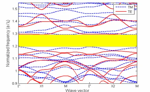
problem in a computation domain equal to a quarter of the unit cell of photonic crystal. The symmetric points of our investigation region in the Brillouin zone are shown in Fig. 2.
The electromagnetic or optical waves in a two-dimensional photonic crystal can be classified by two distinct polarizations. The transverse-electric (TE) modes have the electric field lying in the x-y plane and the transverse-magnetic (TM) modes have the magnetic field lying in the x-y plane. In our simulations, both the TE and TM band diagrams of the photonic crystal are calculated using the fast plane wave expansion method to find the absolute PBG at each iteration step of the SA process. We check the value of PBG of the optimized photonic crystal structure by using 441 plane waves, whereas only 121 plane waves are used during the SA iterations to save computing time.
First, we investigate the optimization of PBG with a fixed filling factor. Here, the filling factor is defined as the ratio of the area occupied by the dielectric material to the total area of a unit cell of the photonic crystal. The optimized photonic crystal and variations of temperature and PBG are shown in Fig. 3. The corresponding band diagram is shown in Fig. 4. The computation domain of this photonic crystal structure is divided into 15×15 pixels, and the filling factor is 0.22. After about 6000 iterations, an absolute PBG (expressed as the normalized frequency a/λ) of 0.098 is obtained. This absolute PBG is in the range from 1.194 to 1.292, i.e., between relative higher-order bands. The gap-midgap ratio here is
about 0.078. We can see from Fig. 3 that the material distribution in the photonic crystal seems to be so complicated. Hence, for a given lattice constant, there still exist many tiny structures in a unit cell. So we would like to consider cases with lower-order absolute PBGs.
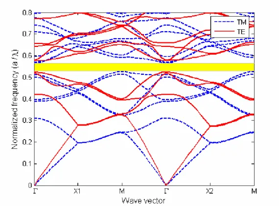
Next, we investigate the optimization of lower-order PBGs with a fixed filling factor. The optimized photonic crystal and variations of temperature and PBG are shown in Fig. 5, with the corresponding band diagram shown in Fig. 6. The computation domain of this photonic crystal structure is divided into 10×10 pixels. The division number of the computation domain here is less than the case in Figs. 3 and 4. Therefore, the final structure of the photonic crystal becomes less complicated. After about 6000 iterations, an absolute PBG of 0.038 is obtained. The absolute PBG is in the range from 0.528 to 0.566, and the gap-midgap ratio is about 0.069. This PBG is smaller than that of Fig. 4. It seems difficult to have a large absolute PBG around lower bands. Since the PBG is distributed in a lower frequency range, the optimized photonic crystal structure becomes simpler than that in Figs. 3 and 4.
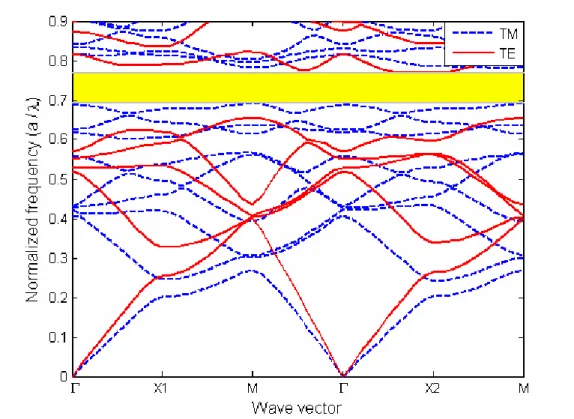
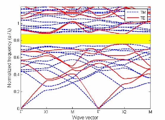
Let us finally consider the optimization of absolute PBG with an adjustable filling factor. The optimized photonic crystal and the corresponding band diagram are shown in Figs. 7 and 8, respectively. After nearly 2000 iterations, we obtain the photonic crystal with absolute PBG between the 14th and 15th bands. As we can see, the absolute PBG is nearly
2.03 times larger than that in Fig. 6. The corresponding gap-midgap ratio is 0.105. It is interesting to modify the cost function in the SA to optimize the gap-midgap ratio in our optimization problem. With a properly designed temperature variation and after 15000 iterations, the optimized photonic crystal and the corresponding band diagram are shown in Figs. 9 and 10, respectively. The gap-midgap ratio is about 0.145 and the corresponding absolute PBG is about 0.119.
Note that the temperature control in the SA is very crucial. We design the temperature variation by trial and error. Generally speaking, the improvement in cost is large at a high temperature, and the temperature should be decreased more rapidly at the early stage. On the other hand, when approaching the nearly optimal solution at a lower temperature, more steps are needed to further improve the cost.
4. CONCLUSIONS
In summary, we have used the simulated annealing algorithm to synthesize 2D photonic crystals for large PBGs. With the aid of the fast plane wave expansion method, much computing time can be saved. By using the SA algorithm, we have synthesized a photonic crystal with a large absolute PBG of 0.119 and the corresponding gap-midgap ratio of 0.145. These photonic crystal structures are composed of only two dielectric materials, which can be practically realized. The study of 2D systems would give us some fundamental sense of synthesizing 3D systems.
ACKNOWLEDGMENTS
This Work was supported by the National Science Council, the Republic of China, under Grant No. NSC 93-2215-E-002-037.
REFERENCES
1. E. Yablonovitch, “Inhibited spontaneous emission in solid-state physics and electronics,” Phys. Rev. Lett. 58, 2059-2062, 1987.
2. S. John, “Strong localization of photons in certain disordered dielectric super lattices,” Phys. Rev. Lett. 58, 2486-2489, 1987.
3. J. D. Joannopoulos, R. D. Mead, and J. N. Winn, Photonic Crystals: Molding the Flow of Light, Princeton University Press, Princeton, 1995.
4. L. Shen, S. He, and S. Xiao, "Large absolute band gaps in two-dimensional photonic crystals formed by large dielectric pixels," Phys. Rev. B 66, 165315, 2002.
5. L. Shen, Z. Ye, and S. He, "Design of two-dimensional photonic crystals with large absolute band gaps using a genetic algorithm," Phys. Rev. B 68, 035109, 2003.
6. R. L. Chern, C. C. Chang, C. C. Chang, and R. R. Hwang, "Large full band gaps for photonic crystals in two dimensions computed by an inverse method with multigrid acceleration," Phys. Rev. E 68, 026704, 2003.
7. S. Preble, M. Lipson, and H. Lipson, “Two-dimensional photonic crystals designed by evolutionary algorithms,” Appl.
Phys. Lett. 86, 061111, 2005.
8. S. Kirkpatrick, C. D. Gelatt Jr., and M. P. Vecchi, “Optimization by simulated annealing,” Science 220, 671–680 1983. 9. N. Metropolis, A. Rosenbluth, M. Rosenbluth, A. Teller, and E. Teller, "Equation of state calculations by fast computing
machines," J. Chem. Phys. 21, 1087-1092, 1953.
1. set initial temperature 2. set initial structure
1. determine the current PBG 2. exchange two pixels with different dielectric constant
3. determine the PBG of the new photonic crystal 4. C1 = PBG(current_structure) - PBG(new_structure)
C1< 0
1. set the current photonic crystal to be the newly modified
photonic crystal
decrease the temperature 1. choose one pixel randomly and change the
dielectric constant to the other value for the current photonic crystal 2. determine the PBG for this newly modified
photonic crystal 3. C2 = PBG(current_structure) - PBG(the newly
modified_structure) C2 < 0 N final temperature Y exp(- C1/T) > random(0,1)
1. set the current photonic crystal to be the new photonic crystal
Y Y
N
Y
N N
Fig. 1. Flow chart for SA algorithms.
2x1OI I-:-0.12 0.11 •
•I.
••I.
••I.
= — — = — — = 0 I 2 x!a 0.1 0.09 63 ci 63 0.08n
0.07 0 a)n
2x10³ a) 0 63 a) ci E a) H 2x10 2x10⁵ 0.03 0 2000 4000 8000 Steps 0.08 0.08 0.04_ _ _
JII
_ _
09 F Xl M F X1 M Wave vectorFig. 2. Symmetric points in the Brillouin zone.
Fig. 3. Photonic crystal structure (left) and plots of variations of temperature and PBG (right).
Fig. 4. Band diagram calculated for photonic crystal structure in Fig. 3.
2x1O 3 2 0.032 a) 0.03 0.028 0 2x10³ a) a) a) ci E a) H
2x10
2x10⁵ a) ci a) 0.028n
a) 0.024 z 0 a)n
0.022 < 0 I 2 3x!a
.02 0.018 0 2000 4000 8000 Steps 0.8 0.7 0.1 0 F Xl M F K? M Wave vectorFig. 5. Photonic crystal structure (left) and plots of variations of temperature and PBG (right).
Fig. 6. Band diagram calculated for photonic crystal structure in Fig. 5.
Temperature
2x10
.11 09 63 3 2 0 0 2 3 2x1032x100
08 63 ci 07 08n
08 004
03 02x!a
Steps 0.9 0.8 0.8 V C a)z 0.6
C
a)0.4
0.3Z 0.2
0.1 0 F Xl M F X1 M Wave vectorFig. 7. Photonic crystal structure (left) and plots of variations of temperature and PBG (right).
Fig. 8. Band diagram calculated for photonic crystal structure in Fig. 7.
3 2 63 0
2x10
•4 •4 •4 2x10³
:.€
:€
2x10
ti't_ti't_tul 2x10
3x!a
2x100
0 0.2 0.18 0.18 0.14 0.12 0.1 0.08 0.08 0.04 0.02 0 1.8 x10⁴ 0.8 I Steps -63;o.8
V C a) C Cr a) 0.8 a) N cr2 xi M Wave vector F x1 MFig. 9. Photonic crystal structure (left) and plots of variations of temperature and gap-midgap ratio (right).
Fig. 10. Band diagram calculated for photonic crystal structure in Fig. 9.