THE
IMPACT
OF
INNER PICKUP
ON
ESD
ROBUSTNESS
OF
MULTI-FINGER
NMOS
IN
NANOSCALE
CMOS
TECHNOLOGY
Ming-Dou Ker and Hsin-Chyh Hsu
Nanoelectronics andGigascale Systems Laboratory, Institute of Electronics
NationalChiao-Tung University, Hsinchu, Taiwan; Tel: (+886)-3-5131573, Fax:(+886)-3-5715412 e-mail: mdker dieee.org, HCHsu dieee.org
ABSTRACT
The impact of pickup structure on ESD robustness of multi-finger MOSFET devices in the nanoscale CMOS process is investigated in this work with 1.2-V and 2.5-V devices in a 130-nm CMOS process. The multi-finger MOSFET device without the pickup structure inserted into its source region can sustain a much higher ESD level and more compactlayoutareaforI/0cells.
[Keywords: electrostatic discharge (ESD), multi-finger MOSFET, layout, pickup structure.]
INTRODUCTION
As CMOS scaling towards nanoscale technologies, ESD
reliability has been amajorconcern ofintegration circuits. In order to sustain the desired ESD robustness, ESD-protectionMOSFET in the ESDprotectioncircuits often has a total channel width of several hundreds micrometer. With such a large device dimension for ESD
protection,the MOSFET devices inI/0celllayoutareoften drawn in the multi-finger structure to save layout area. When the
gate-grounded NMOS (GGNMOS) is under ESD stress, the parasitic
lateral n-p-nbipolarin NMOS device structure will betriggeredinto itssnapback regiontodischargeESD current [1]. However, if one of the parallel multiple fingers is first triggered onduring ESD stress, the ESD current is mainly discharged through the first turned-on
finger. Such non-uniform turned-on issue onmulti-finger MOSFET often decreases its ESDrobustness, evenifthe MOSFET has alarge enoughdevice dimension[2].
However, even ifthe layout of multi-finger NMOS is drawn
uniformly, the equivalentsubstrate resistance of the central fingeris stilllargestbecause the distance from its channelregiontotheguard ring is longest in I/0 layout. Thus, the central finger of the
multi-finger NMOS is often turned on earlier than the other fingers to cause the uniform turned-on issue. In order to solve this non-uniform turned-onproblem,the additionalpickupstructure(inserting
into each source region of the multi-finger NMOS layout) was
reported and recommended toimproveESDrobustness in a0.35-pm
CMOS technology by foundry [3], [4], because all the fingers can have equal equivalent substrate resistance. Thelayouttop view and device cross-sectional view of the additional P+ pickup structure
inserted into the source region ofamulti-finger NMOS device are shown in Figs. l(a)and l(b), respectively. However, the impact of the pickup structures inserted into source regions of multi-finger
NMOS devices on the ESD robustness of MOSFET devices should be furtherinvestigatedinthe nano-scale CMOS process.
DEVICE STRUCTURE
The 1.2-V and 2.5-V devices in a 130-nm salicided CMOS process with different gate-oxide thicknesses are drawn and fabricated in silicon chip. The layout structures of the NMOS, including 1.2-Vand 2.5-V NMOS devices with different numbers(0, 1, 2, and 5)of the P+pickup structures inserted into sourceregions (called as number ofpickups for NMOS) ofmulti-finger NMOS
0-7803-9498-4/06/$20.00020061EEE
devices, are drawn in Figs. 2(a), 2(b), 2(c), and 2(d), respectively.
Each multi-finger NMOS device has 12 parallel fingers, and every finger is drawn with a finger length of 40 ptm. So, the total channel width for eachmulti-finger NMOS device is 480 ptm, and a P+ guard
ringissurroundingthe wholefinger-typeNMOSin thelayout.
EXPERIMENTAL
RESULTS
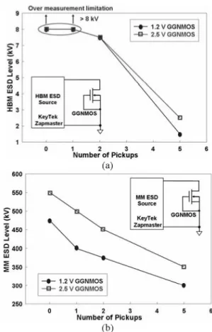
The parasitic lateral bipolar trigger current (Itl), and the snapback holding voltage (Vh) of fabricated MOSFET devices with different number of pickups, are measured by the transmission line pulse (TLP) generator with low energy. The Itl and Vh of the 1.2-V and 2.5-V GGNMOSwith different number ofpickupsarecompared inFigs.3 and 4, respectively. When the number of pickup structures are increased from 0 to 5, the Itl (Vh) is increased in both 1.2-V and 2.5-V devices. The base resistance(Rsub)of theparasiticlateralbipolar
is reduced by the increase of the additional pickup structures, where the distance between the channel regions to the substrate contact becomes shorter. With a low base resistance (Rsub), the parasitic
lateral bipolar in the multi-finger MOSFET needs higher trigger current (Itl) to trigger it on. With an increased snapback holding voltage (Vh),the powerdissipation generated byESD current onthe multi-finger MOSFET becomes higher. These mechanisms cause ESDperformance of multi-finger MOSFET to be seriously decreased when the number of pickup structures increased. TLP-measured
secondary breakdown current(1t2)for 1.2-V and 2.5-Vmulti-finger
GGNMOS with different number ofpickupstructures are compared
inFig. 5. Thedependencesof HBM and MM ESD levels(measured byaZapmaster ESDtester)ondifferent number ofpickupstructures in the multi-finger MOSFET are compared in Figs. 6(a) and 6(b), respectively. The TLP-measured1t2,HBM, and MM ESD levels are confirmed that the increase on the number of pickup structures causes alower ESD robustness on both 1.2-V and 2.5-Vmulti-finger
devices.
CONCLUSION
The degradation of ESD performance due to pickup structures inserted into sourceregions ofmulti-fingerNMOSdevices has been studied in a 130-nm CMOS process. The MOSFET devices with the
pickup structures inserted into the source region are not
recommended inthe nanoscale CMOStechnology. Without adding
the pickup structures in the source regions, the I/0 cell can be realized with more compact silicon area and higherESDrobustness in ICproducts.
REFERENCES
[1]
[2][3]
[4]
631A.Amerasekera etal.,IEDMTech. Dig., 1996,pp. 893-896. T.-L. Polgreenetal.,IEEETrans.Electron Devices,vol. 39,
no.2,pp.379-388,Feb. 1992.
J.-H. Lee etal.,Proc.IPFA, 1999,pp. 162-167. J.-H.Lee, US patent #5,811,856, 1998.
IEEE06CH37728 44th AnnualInternationalReliability Physics
Symposiumr
San Jose, 2006silicide blocking silidd blo
D Gate S
PickUp
S Gate D(a)
Gate Gate Gate Gate~~~~~~~~~~~~~~~~~~~~~~~~~~~~~~~~~~~~~~~~~~~~~~~~~~~~~~~GaeGt
siliideDs Pickup s a
LDD LDDD
P-Well ~~~~~
~~~~~~~~~~~~~~~~~~~~~~~~Rsub
RaubP~Substrate
(b)
FiGuRE1. THE(a)LAYOUT TOPVIEW,AND(b)DEVICE CROSS-SECTIONALVIEW,OFTHENMOSDEVICE WITHTHEADDITIONAL
PICKUPSTRUCTURES INSERTED INTO ITS SOURCE REGIONS.
9' 45i 4I i 25
10
vw' 2.5'GGNMOS WWL- 480pm/Da35 pm + TrkeifCutre flt UtHoldirigVbfte Vh 0 1 2 3 4 Number ofPickupsFIGURE 4. THEPARASITIC LATERAL BIPOLAR TRIGGER CURRENT(IT1)
ANDTHESNAPBACK HOLDING VOLTAGE(VH)OFTHE2.5-V NMOS
WITH DIFFERENT NUMBER(0, 1, 2, 5)OF PICKUPS.
-- 1.2VGGNMOS
a 1 2 3
Number ofPickups 4 5 6
(a) (b)
FIGURE 5. DEPENDENCEOFIT2LEVELON DIFFERENT NUMBER OF PICKUP STRUCTURES OF1.2-VAND2.5-VMULTI-FINGERNMOS.
(c) (d)
FIGURE 2. THELAYOUT TOP VIEW OFTHEMULTI-FINGERMOSFET
WITH DIFFERENT NUMBEROF ADDITIONAL PICKUP STRUCTURES INSERTED INTO SOURCEREGIONS,(a)PICKUP=0, (b)PICKUP=1,
(C)PICKUP=2,AND(d)PICKUP=5.
so g so E! 60 40 0 ?20 I.-I10 0
Overmeasu mre tliairtatn
>s
~~~~~~kV
M ~ ~ ~ 3 . 2 Numbe df Pickups (a) 1I2VGGNMOS 4 6 1,2VGGNMOS WIL 480pmIQ 25pm 4&O 3o0 260 I-- Trigger Cuenit ltiI- IH6IdingVftaolwVh 0 2 NumnberofPickups 4 5s 6 +-1-2VGGNMOS n.5VGGNMOS 1 2 Number o'Pickups (b) 4 5 6
FIGURE 3. THEPARASITIC LATERAL BIPOLAR TRIGGER CURRENT(IT1) ANDTHESNAPBACK HOLDING VOLTAGE(VH)OFTHE1.2-V NMOS
WITH DIFFERENT NUMBER(0, 1, 2, 5)OF PICKUPS.
FIGURE 6. DEPENDENCEOF(a)HBMESDLEVEL, AND(b)MMESD
LEVEL, ON DIFFERENT NUMBER OF PICKUP STRUCTURES OF1.2-VAND2.5-VMULTI-FINGERNMOS.
632 I564. .50 I42 {4A 6 6 W-..