A flexible organic pentacene nonvolatile memory based on high- dielectric layers
Ming-Feng Chang, Po-Tsung Lee, S. P. McAlister, and Albert Chin
Citation: Applied Physics Letters 93, 233302 (2008); doi: 10.1063/1.3046115
View online: http://dx.doi.org/10.1063/1.3046115
View Table of Contents: http://scitation.aip.org/content/aip/journal/apl/93/23?ver=pdfcov Published by the AIP Publishing
Articles you may be interested in
Design rules of (Mg,Zn)O-based thin-film transistors with high- WO 3 dielectric gates Appl. Phys. Lett. 101, 183502 (2012); 10.1063/1.4764559
Strain induced anisotropic effect on electron mobility in C 60 based organic field effect transistors Appl. Phys. Lett. 101, 083305 (2012); 10.1063/1.4747451
ZnO-based low voltage inverter with low- k /high- k double polymer dielectric layer Appl. Phys. Lett. 93, 193514 (2008); 10.1063/1.3028093
Pentacene-based thin film transistors with titanium oxide-polystyrene/polystyrene insulator blends: High mobility on high K dielectric films
Appl. Phys. Lett. 90, 062111 (2007); 10.1063/1.2450660
High- k and low- k nanocomposite gate dielectrics for low voltage organic thin film transistors Appl. Phys. Lett. 88, 243515 (2006); 10.1063/1.2213196
This article is copyrighted as indicated in the article. Reuse of AIP content is subject to the terms at: http://scitation.aip.org/termsconditions. Downloaded to IP: 140.113.38.11 On: Wed, 30 Apr 2014 07:41:52
A flexible organic pentacene nonvolatile memory based on
high-
dielectric layers
Ming-Feng Chang,1Po-Tsung Lee,1S. P. McAlister,2and Albert Chin3,4,a兲
1Department of Photonics and Institute of Electro-Optical Engineering, National Chiao-Tung University,
Hsinchu 300, Taiwan
2National Research Council of Canada, Ottawa ON K1A OR6, Canada
3Department of Electronics Engineering, National Chiao-Tung University, Hsinchu 300, Taiwan 4
Nano-Electronics Consortium of Taiwan, Hsinchu 300, Taiwan
共Received 8 September 2008; accepted 20 November 2008; published online 10 December 2008兲 We report a pentacene thin film transistor nonvolatile memory fabricated on a flexible polyimide substrate. This device shows a low program/erase voltage of 12 V, a speed of 1/100 ms, an initial memory window of 2.4 V, and a 0.78 V memory window after 48 h. This has been achieved by using a high- dielectric as charge trapping, blocking, and tunneling gate insulator layers. © 2008
American Institute of Physics. 关DOI:10.1063/1.3046115兴
Organic nonvolatile memory devices have potential ap-plications in flexible display drive logic, radio frequency identification tags, and smart cards.1,2 These nonvolatile memory devices supply an essential function for integrated circuits共ICs兲 based on organic thin-film transistors 共OTFTs兲. The advantages of using organic memory devices, over their inorganic counterparts, are in their low cost, light weight, simple structure, mechanical flexibility, and low-temperature processing. For system-on-chip application, the nonvolatile memory function is required. The OTFT-based nonvolatile organic memory devices display high drive current, low off-state leakage current, and reasonably fast switching speeds. The memory properties of these OTFT-based devices arise from the electric field modulation in the gate insulator through the spontaneous polarization of ferroelectrics2–4 or because of charge trapping in a chargeable layer.5,6 The charge-trapping type of OTFT memory device employs the well-known device physics of such structures and can build on the manufacturing experience of the Si industry. Digital data can be programed into the device by injecting charges into the gate insulator or erased by removing the stored charges. This charge transfer in the gate dielectric is readable by measuring the threshold voltage 共Vth兲 of the transistor. This program or erase function can be obtained by having a large electric field across the gate insulator. Previous charge-trapping OTFTs have used a polymer as the charge-trapping layer5 or a floating gate,6necessitating a high gate voltage共Vg兲 to
write the data. Such high voltages are incompatible with low-power IC designs and challenge existing battery technol-ogy. A solution to lowering the program and erase voltages is to use a high-dielectric. This has been done by incorporat-ing a high- dielectric as the gate insulator in the OTFTs, leading to lower voltage operation.7–9
A schematic diagram of the OTFT nonvolatile memory is shown in Fig.1共a兲. The OFET memory devices were fab-ricated on 125 m thick polyimide 共PI兲 substrates 共Kapton HPP-ST, Dupont兲. Prior to device fabrication, the substrates were cleaned in de-ionized water and annealed in a vacuum 共3⫻10−6 torr兲 at 200 °C to improve the dimension stability. A 100 nm SiO2 thin film was deposited on the substrate by
electron beam evaporation to create a layer with low internal stress. A 50 nm TaN gate electrode was then deposited by reactive sputtering through a shadow mask. This was given a NH3+plasma treatment to improve the metal-electrode/high- interface.9The 20 nm HfLaO, 20 nm HfON, and 6 nm HfO2 were then deposited by physical vapor deposition and given a 200 ° C, 30 min furnace treatment in O2 to improve the gate oxide quality. This was followed by deposition through a shadow mask of the pentacene active layer 共Aldrich Chemical Co.兲 that was 70 nm thick. 共The deposition condi-tions were as follows: a deposition rate of 0.5 Å/s at a pres-sure of 3⫻10−6 torr, with the substrate being held at 70 ° C.兲 Finally, 50 nm of gold was deposited at rate of
a兲Electronic mail: [email protected].
FIG. 1. 共a兲 Schematic cross-sectional diagram of the flexible pentacene OTFT memory devices. 共b兲 Transfer characteristics of pentacene OTFT memory devices.
APPLIED PHYSICS LETTERS 93, 233302共2008兲
0003-6951/2008/93共23兲/233302/3/$23.00 93, 233302-1 © 2008 American Institute of Physics
This article is copyrighted as indicated in the article. Reuse of AIP content is subject to the terms at: http://scitation.aip.org/termsconditions. Downloaded to IP: 140.113.38.11 On: Wed, 30 Apr 2014 07:41:52
1 Å/s for the source/drain electrodes. The channel width and channel length were 1500 and 150 m, respectively. All electrical characteristics were made using an HP4156C semi-conductor parameter analyzer and an HP4284A precision
LCR meter in the dark and an air ambient.
The transfer characteristics for OTFT memory device are displayed in Fig. 1共b兲. From the transfer characteristics, the mobility Vth, subthreshold swing 共SS兲, and on/off current ratio 共Ion/Ioff兲 were 0.1 cm2/V s, −1.4 V, 160 mV/decade, and 1⫻104in the saturation region at a drain voltage共V
d兲 of
−3 V. The low Vth and good SS are due to the use of a high- material as gate dielectric.7–9
The energy band diagram of our OTFT memory device is shown in Fig.2.10–12The HfLaO gate dielectric has a high dielectric constant, large bandgap, and high electron injec-tion barrier with respect to the TaN gate electrode during the erase process.9A proper thickness of HfLaO blocking layer is important to reduce gate leakage current. The higher gate leakage current will degrade the mobility, SS, and retention time of OTFT memory devices. The small band-gap HfON12–14 with its deep trapping energy was chosen as the charge-trapping layer to achieve good charge trapping char-acteristics. The thin HfO2 dielectric serves as a charge-tunneling layer and charge-blocking layer. The gold elec-trode forms an Ohmic-like contact for the injection of holes. When a proper gate bias is applied, the charges in the pen-tacene active layer tunnel through the HfO2 are trapped in the HfON layer.
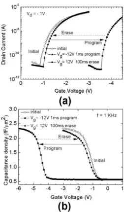
In Fig.3, we show the shift in the transfer characteristics at Vd= −1 V, under a gate bias of −12 V at 1 ms for the
program, and +12 V at 100 ms for the erase process. The drain current-gate voltage共Id-Vg兲 curve shifted in a negative
direction when a Vgof −12 V was applied for 1 ms, and in
a positive direction after application of a reverse Vgof 12 V
for 100 ms. Thus the Vthvalue can be shifted reversibly by applying an appropriate gate bias. A 2.6 V Vth shift was shown after a −12 V program voltage pulse was applied for 1 ms. This could be erased with a large 2.5 V Vthshift after a +12 V voltage pulse for 100 ms. Since a negative voltage was applied across the HfLaO/HfON/HfO2 gate dielectric stack during the programing process, hole accumulation oc-curred at the dielectric/pentacene interface. The increase in the Vth shift with the increase in negative Vg indicates that
the accumulated holes were injected over the HfO2 gate di-electric and stored in the lower energy HfON didi-electric. The erase was performed by applying a positive Vg to the TaN
gate electrode, where the applied electric field over the
HfLaO/HfON/HfO2 gate dielectric stack causes hole depletion in the pentacene. The stored holes in the HfON may tunnel out over the HfO2 gate dielectric into the pentacene; alternatively, the minority carriers 共electrons兲 generated in the depletion region of the pentacene can also tunnel through the HfO2 and into the HfON, all of which give rise to the erase function. Similar mechanisms have also been suggested by us to explain the program and erase functions in Si-based nonvolatile memory.12–16 The shift in capacitance-voltage characteristics for a TaN– HfLaO– HfON– HfO2-pentacene-Au metal-insulator-semiconductor capacitor is shown in Fig. 3共b兲.
For nonvolatile memory applications, good retention characteristics are essential. To investigate the retention, we applied a Vg of −12 V at 1 ms to program the device and
FIG. 2. 共Color online兲 Band diagram of the
TaN– HfLaO– HfON– HfO2-pentacene-Au OTFT.
FIG. 3. 共a兲 Drain current-gate voltage 共Id-Vg兲 hysteresis curves for a
pentacene OTFT memory device under Vg= −12 V, 1 ms program and
Vg= −12 V, 100 ms erase conditions. The Id-Vg curves were measured
at Vd= −1 V. 共b兲 Capacitance-voltage hysteresis curves for a
TaN– HfLaO– HfON– HfO2-pentacene-Au metal-insulator-semiconductor
capacitor.
FIG. 4. Retention characteristics in terms of the threshold voltage共Vth兲 for
the memory device for Vg= −12 V, 1 ms program and Vg= 12 V, 100 ms
erase conditions.
233302-2 Chang et al. Appl. Phys. Lett. 93, 233302共2008兲
This article is copyrighted as indicated in the article. Reuse of AIP content is subject to the terms at: http://scitation.aip.org/termsconditions. Downloaded to IP: 140.113.38.11 On: Wed, 30 Apr 2014 07:41:52
12 V at 100 ms for the erase function. In Fig.4, we show the retention data. The Vthwas extracted in the linear region of the Id-Vg characteristics at Vd= −1 V. The initial memory
window was 2.4 V, which decreased to 0.78 V after 48 h. The significant charge loss of⬃50% at 103 s is possibly related to the increase in the leakage current due to the surface roughness of the PI substrates, as well as defects in the low-temperature-formed HfO2. Atomic force microscopy showed that the rms surface-roughness was approximately 5 nm. Im-provements in the leakage current can be expected from smoother substrates and replacing the HfO2 with a higher-quality gate dielectric.
In summary, we have fabricated organic pentacene non-volatile OTFT memory devices on flexible PI substrates. These devices used a high- HfON dielectric as the charge trapping layer, HfLaO as blocking layers and HfO2 as the tunneling layer. We found program/erase voltages of −12/12 V, at a speed of 1/100 ms along with an initial memory window of 2.4 V.
This work has been supported in part by NSC Contract No. 97-2120-M-009-008.
1J. C. Scott and L. D. Bozano, Adv. Mater.共Weinheim, Ger.兲 19, 1452
共2007兲.
2R. Schroeder, L. A. Majewski, and M. Grell, Adv. Mater. 共Weinheim,
Ger.兲 16, 633共2004兲.
3R. C. G. Naber, C. Tanase, P. W. M. Blom, G. H. Gelinck, A. W.
Mars-man, F. J. Touwslager, S. Setayesh, and D. M. de Leeuw,Nature Mater. 4,
243共2005兲.
4R. C. G. Naber, P. W. M. Blom, G. H. Gelinck, A. W. Marsman, and D. M.
de Leeuw,Adv. Mater.共Weinheim, Ger.兲 17, 2692共2005兲.
5M. Mushrush, A. Facchertti, M. Lefenfed, H. E. Katz, and T. J. Marks,J.
Am. Chem. Soc. 125, 9414共2003兲.
6K.-J. Baeg, Y.-Y. Noh, J. Ghim, S.-J. Kang, H. Lee, and D.-Y. Kim,Adv.
Mater.共Weinheim, Ger.兲 18, 3179共2006兲.
7C. D. Dimitrakopoulos, S. Purushothaman, J. Kymissis, A. Callegari, and
J. M. Shaw,Science 283, 822共1999兲.
8L. A. Majewski, R. Schroeder, and M. Grell, Adv. Mater. 共Weinheim,
Ger.兲 17, 192共2005兲.
9M. F. Chang, P. T. Lee, S. P. McAlister, and A. Chin, IEEE Electron
Device Lett. 29, 215共2008兲.
10J. Robertson,J. Vac. Sci. Technol. B 18, 1785共2000兲.
11V. V. Afanas’ev, S. Shamuilia, A. Stesmans, A. Dimoulas, Y. Panayiotatos,
A. Sotiropoulos, M. Houssa, and D. P. Brunco, Appl. Phys. Lett. 88,
132111共2006兲.
12H. J. Yang, C. F. Cheng, W. B. Chen, S. H. Lin, F. S. Yeh, S. P. McAlister,
and A. Chin,IEEE Trans. Electron Devices 55, 1417共2008兲.
13H. J. Yang, A. Chin, W. J. Chen, C. F. Cheng, W. L. Huang, I. J. Hsieh, S.
P. McAlister, IEEE Electron Device Lett. 28, 913共2007兲.
14H. J. Yang, A. Chin, S. H. Lin, F. S. Yeh, and S. P. McAlister, IEEE
Electron Device Lett. 29, 386共2008兲.
15X. Wang, J. Liu, W. Bai, and D.-L. Kwong,IEEE Trans. Electron Devices 51, 597共2004兲.
16C. H. Lai, B. F. Hung, A. Chin, W. J. Yoo, M. F. Li, C. Zhu, S. P.
McAlister, and D. L. Kwong,IEEE Electron Device Lett. 26, 148共2005兲.
233302-3 Chang et al. Appl. Phys. Lett. 93, 233302共2008兲
This article is copyrighted as indicated in the article. Reuse of AIP content is subject to the terms at: http://scitation.aip.org/termsconditions. Downloaded to IP: 140.113.38.11 On: Wed, 30 Apr 2014 07:41:52