Investigation of LaAlO
3/ZrO
2/a-InGaZnO
thin-film transistors using atmospheric
pressure plasma jet
Chien-Hung Wu, Hau-Yuan Huang, Shui-Jinn Wang,
Kow-Ming Chang and Hsin-Yu Hsu
Amorphous indium–gallium–zinc-oxide thin-film transistors (a-IGZO-TFTs) with the LaAlO3/ZrO2gate dielectric stack employing a novel
atmospheric pressure plasma jet process that results in small subthres-hold swing and low thressubthres-hold voltage are proposed and fabricated. The influence of post-deposition annealing (PDA) temperature on LaAlO3/
ZrO2gate dielectric stack and device performance was investigated.
The equivalent oxide thickness of the LaAlO3/ZrO2dielectric stack
decreases from 11.5 nm without annealing to 7 nm after a 500°C annealing was applied. The LaAlO3/ZrO2/a-InGaZnO TFT with a
500°C annealing exhibits a small subthreshold swing of 77 mV·dec−1, a highfield-effect mobility of 9 cm2·V−1·s−1and an
excellent current ratio of 1.8 × 10⁷, which could be attributed to the improved gate dielectric quality by the PDA. The LaAlO3/ZrO2
/a-InGaZnO TFTs with excellent gate control ability allow the device to operate at a low operating voltage with low power consumption.
Introduction: Of the abundant AOS compound materials, amorphous indium–gallium–zinc-oxide thin-film transistors (a-InGaZnO TFTs) attract considerable interest for backplanes of the next-generation flat-panel displays as active matrix liquid crystal displays and active matrix organic light-emitting diode displays. Owing to their better field-effect mobility >10 cm2
/V·s and better stability against electrical stress [1, 2]. The non-vacuum techniques such as solution-processed InGaZnO films [3, 4] and atmospheric pressure plasma jet (APPJ) InGaZnO films were proposed recently [5, 6]. The APPJ technique has lower apparatus cost since it does not need a vacuum chamber and associated pumping systems; it also has better suitability for large-scale applications among the other deposition technologies. To further improve the device performance, high-κ materials of ZrO2and HfO2have been investigated for their superior properties for advanced TFT devices, such as high breakdownfield intensity (10∼15 MV/cm), high dielectric constant (20∼25) and the capability of room-temperature processing [7, 8]. In this Letter, the fabrication of bottom-gate IGZO-TFTs with an LaAlO3/ZrO2gate dielectric stack (40 nm/10 nm) is reported. The equivalent oxide thickness (EOT) of the LaAlO3/ ZrO2 dielectric stack shrinks from 11.5 nm before post-deposition annealing (PDA) to 7 nm after a 500°C PDA. Excellent gate control ability with a small subthreshold swing (SS) of 77 mV·dec−1, high field-effect mobility (μfet) of 9 cm2V−1·s−1, high current ratio (Ion/ Imin) of 1.8 × 10⁷and low operation voltage of 3.0 V are attributed to the improved gate dielectric quality by the PDA.
Experiments: Fig. 1 shows the schematic of the fabricated LaAlO3 (40 nm)/ZrO2(10 nm)/IGZO (50 nm) TFT. The staggered bottom-gate a-IGZO-TFTs were fabricated on heavily doped n-type silicon sub-strates. High-κ gate dielectrics of LaAlO3and ZrO2were deposited by an e-beam evaporation with thicknesses of 40 and 10 nm, respectively, on the silicon substrate which served as the gate electrode. PDA was then carried out at various temperatures (T ) between 300 and 500°C
in N2 for 10 min. Subsequently, a 50 nm-thick a-IGZO layer was
deposited by APPJ. The substrate temperature was kept at 200°C during deposition of InGaZnO. Trimethylaluminium (Al2(CH3)6, TMA) and oxygen plasma reactants were used as precursors and oxidants, respectively. Indium nitrate (In(NO3)2), gallium nitrate (Ga(NO3)2) and zinc nitrate (Zn(NO3)2) were used as the precursor materials. The concentration of the InGaZnO solution was kept at 0.2 M and was ultrasonically atomised at 2.45 MHz into mist and then conveyed by the carrier gas (N2) to the plasma region connected to a pulsed DC power supply at a repetition rate of 25 kHz and voltage pulse of 15 kV with a pulse width of 8μs to generate the down-stream plasma. The InGaZnOfilm was deposited and patterned through photolithography and wet etching. Finally, 300 nm-thick Al source/ drain contacts were thermally deposited and formed by the lift-off. The channel width (W ) and length (L) were 200 and 20μm, respect-ively. Al/LaAlO3/ZrO2/p-Si (MIS structure) capacitors were fabricated simultaneously for C–V performance characterisation. The devices were characterised under an open air condition at room temperature using a semiconductor parameter analyser (2636A, Keithley, USA).
Al 20 µm Al
APPJ InGaZnO (50 nm)
LaAlO3 (40 nm) ZrO2 (10 nm)
n+ Si-sub
Fig. 1 Schematic diagram of bottom-gate ZrO2/LaAlO3/IGZO-TFT
Results and discussion: The optical transmittance spectra of the a-IGZOfilms deposited on a glass substrate are shown in Fig.2. The average transmittance of a-IGZOfilms on a glass substrate are more than 80% in the visible range. The transmittance spectrum of the glass substrate is also indicated. In a direct-transition semiconductor, the absorption coefficient, α, and optical band gap (Eg) are related by Tang et al. [9] as follows: α2= B(hν–Eg) and α = 2.303[log(1/T )]/d, where B is a constant, hν is the energy of the incident photon and T and d are the transmittance and thickness of the thinfilms. The band gap of a-IGZOfilms is about 3.35 eV.
300 450 600 750 900 0 20 40 60 80 100
50 nm-thick a-IGZO by APPJ
transmittance, %
l, nm glass IGZO/glass
Fig. 2 Optical transmission spectra of 50 nm-thick a-IGZO film on glass substrates by APPJ
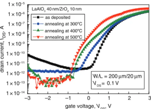
The C–V characteristics of the Al/LaAlO3/ZrO2/p-Si (MIS structure) are shown in Fig. 3. The capacitance of the Al/LaAlO3/ZrO2/p-Si capacitor increases with an increasing PDA temperature. The calculated EOTs of the LaAlO3/ZrO2dielectric stacks are 11.5, 10, 9 and 7 nm for the case without PDA and at annealing temperatures of 300, 400 and 500°C, respectively. The decrease in theflat-band voltage and increase in the slope with increasing T indicates that both the interface and the bulk traps of the dielectric stack are recovered by the high annealing temperature. With a sharper slope and a considerable shift towards posi-tive VG-axis for the Vfb, an improved LaAlO3/ZrO2 gate dielectric quality could be obtained. The transfer curves of the IGZO-TFTs without and with the annealing temperatures of 300, 400 and 500°C are shown in Fig.4. It is noted that the current maximum (Imax) increases with increasing T, while the current minimum (Imin) reduces to about 10−13A. The current ratio (Imax/Imin) and the threshold voltage (Vt) are 4.7 × 10⁵and 1.0 V, 1.2 × 10⁶and 0.8 V, 5.2 × 10⁶and 0.5 V, and 1.8 × 10⁷and 0.1 V for the case without PDA and T = 300, 400 and 500°C. The μfet and SS were extracted through the dependences of Lgm/CiWVDSandδVGS/δ(log IDS), which are 8.3 cm2/V·s and 219 mV/ dec, 7.8 cm2/V·s and 335 mV/dec, 8 cm2/V·s and 109 mV/dec, and 9 cm2/V·s and 77 mV/dec for the case without PDA and T = 300, 400 and 500°C. The improved SS at high T could be attributed to the increased gate oxide capacitance (Cox) and therefore the higher κ value of the LaAlO3/ZrO2dielectric stack by the PDA; however, the deviation of SS andμfetat 300 and 400°C could be induced by the incre-ment of interface traps since the annealing was applied before channel deposition, and a constant channel capacitance can be assumed [10]. The best device performances of Imax/Imin, SS, Vtandμfetare 1.8 × 10⁷, 77 mV/dec, 0.1 V and 9 cm2/V·s, respectively, which were obtained for the case with T = 500°C. The comparisons of the ZrO2/ LaAlO3/IGZO-TFT with variant gate dielectric stacks are shown in Table1.
–6 –5 –4 –3 –2 –1 0 1 2 3 0 0.1 0.2 0.3 0.4 0.5 0.6 LaAlO3 40nm/ZrO2 10nm capacitance density, µ F/cm 2 voltage, V as deposited annealing at 300ºC annealing at 400ºC annealing at 500ºC
Fig. 3 C–V characteristics of Al/LaAlO3/ZrO2/p-Si (MIS structure) gate
capacitor annealed at different PDA temperatures
LaAlO3 40nm/ZrO2 10nm –3 –2 –1 0 1 2 3 1 × 10–14 1 × 10–13 1 × 10–12 1 × 10–11 1 × 10⁻¹⁰ 1 × 10⁻⁹ 1 × 10⁻⁸ 1 × 10⁻⁷ 1 × 10⁻⁶ 1 × 10⁻⁵ W/L = 200µm/20µm VDS= 0.1V gate voltage, VGS, V drain current, IDS , A as deposited annealing at 300ºC annealing at 400ºC annealing at 500ºC
Fig. 4 IDS–VGStransfer characteristics of IGZO-TFT with LaAlO3(40 nm)/
ZrO2(10 nm) dielectric stack at different PDA temperatures
Table 1: Comparisons of LaAlO3/ZrO2/a-IGZO-TFT with variant gate dielectric stacks
Dielectric materials Mobility
(cm2
/V·s) Vt(V) SS (mV/dec) Imax/Imin
PVD LaAlO3/ZrO2, this work 9 0.1 77 1.8 × 10⁷
PE-ALD Al2O3[5] 8.4 0.7 280 1.0 × 10⁸
AP-CVD AlOx[6] 4.2 3.6 550 ∼108
RF sputter ZrO2[7] 28 3.2 560 4.8 × 10⁷
RF sputter HfON/HfO2/HfON [8] 10.2 −0.92 130 2.2 × 10⁶
Conclusion: LaAlO3/ZrO2/a-IGZO-TFTs with a silicon gate have been fabricated successfully using the APPJ process. The devices feature a small SS of 77 mV·dec−1, a highμFETof 9 cm2·V−1·s−1 and a good Imax/Iminof 1.8 × 10⁷with 500°C annealing of the LaAlO3/ZrO2 dielec-tric stack. The integration of high-κ LaAlO3/ZrO2 dielectrics into IGZO-TFTs attains the aim of enhancing the gate control ability. It is expected that LaAlO3/ZrO2/a-IGZO-TFTs might have great potential for applications in low power-consuming and high-end displays. Acknowledgments: This work was supported by the National Science
Council of Taiwan, Republic of China, under grants NSC
100-2221-E-006-156-MY2, NSC 100-2221-E-006-045-MY2 and NSC
102-2221-E-006-217-MY2. The authors thank the Center for Micro/ Nano Science and Technology, National Cheng Kung University, Taiwan, for equipment access and technical support.
© The Institution of Engineering and Technology 2014 7 March 2014
doi: 10.1049/el.2014.0816
One or more of the Figures in this Letter are available in colour online. Chien-Hung Wu (Department of Electronics Engineering, Chung Hua University, Hsinchu, Taiwan)
E-mail: [email protected]
Hau-Yuan Huang and Shui-Jinn Wang (Department of Electrical Engineering, Institute of Microelectronics, National Cheng Kung University, Tainan, Taiwan)
Kow-Ming Chang and Hsin-Yu Hsu (Department of Electronics Engineering, National Chiao Tung University, Hsinchu, Taiwan) References
1 Bak, J.Y., Yoon, S.M., Yang, S., Kim, G.H., Park, S.H.K., and Hwang, C.S.: ‘Effect of In-Ga-Zn-O active layer channel composition on process temperature forflexible oxide thin-film transistors’, J. Vac. Sci. Technol. B, 2012, 30, (4), pp. 041208-1–6
2 Lee, Y.S., Chen, W.J., Huang, J.S., and Wu, S.C. :‘Effects of compo-sition on optical and electrical properties of amorphous in–Ga–Zn–O films deposited using radio-frequency sputtering with varying O2gas
flows’, Thin Solid Film, 2012, 520, pp. 6942–6946
3 Kim, C.E., Cho, E.N., Moon, P., Kim, G.H., Kim, D.L., Kim, H.J., and Yun, I.:‘Density-of-states modeling of solution-processed InGaZnO thin-film transistors’, IEEE Electron Device Lett., 2010, 31, (10), pp. 1131–1133
4 Yang, Y.H., Yang, S.S., and Chou, K.S.:‘Characteristic enhancement of solution-processed In–Ga–Zn oxide thin-film transistors by laser annealing’, IEEE Electron Device Lett., 2010, 31, (9), pp. 969–971 5 Wu, C.H., Chang, K.M., Huang, S.H., Deng, I.C., Wu, C.J., Chiang, W.
H., and Chang, C.C.:‘Characteristics of IGZO TFT prepared by atmos-pheric pressure plasma jet using PE-ALD Al2O3 gate dielectric’, IEEE Electron Device Lett., 2012, 33, (4), pp. 552–554
6 Furuta, M., Kawaharamura, T., Wang, D., Toda, T., and Hirao, T.: ‘Electrical properties of the thin-film transistor with an indium– gallium–zinc oxide channel and an aluminium oxide gate dielectric stack formed by solution-based atmospheric pressure deposition’, IEEE Electron Device Lett., 2012, 33, (6), pp. 851–853
7 Lee, J.S., Chang, S., Koo, S.-M., and Lee, S.Y.:‘High-performance a-IGZO TFT with ZrO2gate dielectric fabricated at room temperature’,
IEEE Electron Device Lett., 2010, 31, (3), pp. 225–227
8 Yuan, L., Zou, X., Fang, G., Wan, J., Zhou, H., and Zhao, X.: ‘High-performance amorphous indium gallium zinc oxide thin-film transistors with HfOxNy/HfO2/HfOxNytristack gate dielectrics’, IEEE
Electron Device Lett., 2011, 32, (1), pp. 42–44
9 Tang, Z.K., Wong, G.K.L., Yu, P., Kawasaki, M., Ohtomo, A., Koinuma, H., and Segawa, Y.: ‘Room temperature ultraviolet laser emission from self-assembled ZnO microcrystallite thinfilms’, Appl. Phys. Lett., 1998, 3270, (72), pp. 3270–3272
10 Su, N.C., Wang, S.J., and Chin, A.:‘High performance InGaZnO thin film transistors using HfLaO gate dielectric’, IEEE Electron Device Lett., 2009, 30, (12), pp. 1317–1319