DOI 10.1007/s00170-005-2571-7
O R I G I N A L A R T I C L E
Kuen Ming Shu · Hung Rung Shih · G.C. Tu
Electrical discharge abrasive drilling of hard materials
using a metal matrix composite electrode
Received: 22 March 2004 / Accepted: 15 January 2005 / Published online: 16 November 2005 ©Springer-Verlag London Limited 2005
Abstract The main object of the present work was to develop an electrical discharge abrasive drilling (EDAD) methodology to remove the re-solidified layer through the grinding induced by a metal matrix composite electrode prior to the re-solidification of molten material. A metal matrix composite (Cu/SiCp) elec-trode, with an electroless pretreatment of Cu coating on SiCpto enhance bonding status between Cu and SiCp, was made with a rotating device and this was employed to study the EDAD tech-nology. The machinability of the mold steel HPM50 and tung-sten carbide P20 was investigated by the combined technologies of EDAD. The machined surfaces of these materials were exam-ined by scanning electron microscopy (SEM) and their surface roughness measured by a profilemeter. From the experimental results, it was found that the EDAD machining efficiency was three to seven times than that of normal EDM operation for mold steel. However, the efficiency improvement is hardly detectable for tungsten carbide. In addition, the surface roughness of both materials could be improved in comparison with that achieved after EDM.
Keywords Cu/SiCpcomposite· Electrical discharge abrasive drilling· Material removal rate · Surface roughness
1 Introduction
Electrical discharge machining (EDM) has been shown to be a versatile method for machining difficult-to-work material in-K.M. Shu (u) · H.R. Shih
Department of Mechanical Manufacturing Engineering, National Formosa University,
Hu-wei, Yunlin, Taiwan, R.O.C. E-mail: kmshu@sunws.nfu.edu.tw Tel.: +886-5-6315327
Fax: +886-5-6315310 G.C. Tu
Department of Materials Science and Engineering, National Chiao Tung University,
Hsinchu, Taiwan, R.O.C.
cluding heated-treated steels, tungsten carbides and various con-ductive ceramics [1–3]. However, low machining efficiency is one of the main EDM disadvantages. At present, many effica-cious hybrid machining technique are employed to enhance the material removal rate (MRR) and/or surface roughness in EDM. Electrochemical discharge machining (ECDM) is a hybrid tech-nology that incorporates ECM and EDM [4], ten times of MRR greater than that of conventional grinding for materials harder than HRc 60 can be obtained by this method [5]. Ultrasonic ma-chining (USM) combined with EDM has been found to increase the MRR in machining hard materials like titanium alloy, tung-sten carbide, titanium boride, etc [6–9].
The concept of combining EDM and diamond grinding for machining electrically conducting hard materials originated in the former USSR [10–12]. The process termed electrical discharge diamond grinding (EDDG) utilizes a metal bonded diamond-grinding wheel and subjects the work to the simultan-eous influence of diamond grains and electrical sparks which cause abrasion and surface melting respectively.
Electro discharge dressing is a new method for dressing the diamond wheel that was glazed by intense wear attritions when grinding hard material. A maximum protrusion height close to 60% of the diamond grain size is achieved by this method [13]. In EDDG, it represents continuous in-process dressing of the grinding wheel, as material is eroded from the electrode as well. This obviates the need to interrupt machining for dressing the wheel. However, the EDDG can’t be popularized because of the high loss of diamond wheel material and the production cost.
When the current flow ceases in EDM, a violent collapse of the plasma channel and vapor bubble causes superheated molten liquids on both the workpiece and electrode surfaces to explode into the gap, and the dielectric liquid solidifies the molten terial immediately. However, the majority of the molten ma-terial cannot be removed because of its surface tension and bonding status between liquid and solid. The molten material remaining on the workpiece surface is cooled by the dielec-tric liquid, forming the recasted zone, and hence creates crater, ridge, and protrusion morphologies as observed on the EDMed surfaces [14].
The main object of the present work was to develop an electrical discharge machining and grinding (EDAD) methodol-ogy to remove the protrusion through the grinding induced by a metal matrix composite electrode prior to the protrusion’s so-lidification. To carry out the EDAD operation, there is clearly a need to have a high conductivity metal matrix composite elec-trode with anti-wear abrasive particles. Methods for fabricating metal based composite materials include melting and casting, co-precipitation, internal oxidation, and powder metallurgy [15]. Owing to the poor dispersion between metal and reinforcements, the melting and casting methods are impractical. The methods of co-precipitation and internal oxidation are not suitable for mass production; therefore, the powder metallurgy method, being ca-pable of mass production, is the preferred choice in fabricating the composite electrode for the purpose of EDAD. For enhancing the bonding status between matrix and reinforcement of compos-ite electrode, electroless copper plating on reinforcement surface is adopted in this research.
2 Experimental procedure
Metal matrix composites can be placed into three categories – particulate, fiber, and laminar – based on the shapes of the reinforced materials. The particulate composites contain large amounts of coarse particles that do not effectively block slip. SiCpwas selected as the reinforcement in this experiment for its superior mechanical properties of high hardness, high anti-wear stiffness during the grinding operation, high electrical conduc-tivity to comply with the international annealed copper standard (IACS) electrode standard, and high thermal conductivity to ob-tain higher thermal shock resistance. Copper was selected as the matrix material for its high electric conductivity. The above-mentioned properties are all necessary for the EDAD electrode application.
The workpieces used in this study are P20 (Mitsubishi Co.) tungsten carbide and HPM 50 (Hitachi Co.) mold steel with a 4 mm hole through the center. The hole is created to ensure that the whole workpiece facing the electrode of 8 mm diameter is undergoing EDAD operation. The chemical compositions of the workpieces are shown in Table 1 and Table 2, respectively. Fig. 1a shows the microstructure of P20 after etching in
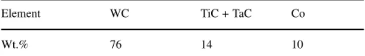
Mu-Table 1. The chemical composition of P20 tungsten carbide
Element WC TiC + TaC Co
Wt.% 76 14 10
Table 2. The chemical composition of HPM50 mirror mold steel
Element C Si Mn Ni Al Cu Mo Fe
Wt.% 0.05-0.18 0.15-1.0 1.0-2.0 2.5-3.5 0.5-1.5 0.7-1.5 0.1-0.4 bal
Fig. 1a,b. Micrographs of the mold material: a P20 WC and b HPM 50 mold steel
rakami’s reagent (10 g K3Fe(CN)6, 10 g KOH, and 100 ml water)
for 10 s; the etching outlines the carbide grains and darkens them slightly, while the Co binder is unaffected. Figure 1b shows the microstructure of HPM 50 after etching in 2% nital (2%HNO3,
98%C2H5OH) solution; the etching attacks both ferrite grain
boundaries (dark line) and the ferrite-cementite spheroid phase within grain. Not all the ferrite grain boundaries are clearly etched because of the orientation sensitivity of nital.
The EDAD processes were performed using a charm CM240C die-sinking machine. Table 3 lists the correlated para-metric values or ranges adopted in this study.
The experimental set up of the EDAD process is schemati-cally shown in Fig. 2. One of the primary objectives was to study the effect of electrode rotation. Therefore, a rotating facility was developed to allow the electrode to rotate at 0–2500 rpm. The electrode was rotated and sunk simultaneously to machine the
Table 3. Design scheme of experimental parameters for EDAD Electrical discharge machining and grinding conditions Work condition Description
Workpiece P20 WC and HPM 50 mirror mold steel Electrode Cu/SiCpcomposite,φ 8 mm
Polarity (electrode) Negative Peak current (Ip) 1–5 A
Pulse duration (τon) 125µs
Pulse off time (τoff) 125µs
Duty factor 0.5 Rotating speed (s) 0∼ 2500 rpm
Dielectric fluid CASTROL SPE oil. Flushing pressure 2 kg/cm2
Fig. 2. Schematic experimental setup for EDAD process
workpiece. When the EDAD operation was introduced, as shown in Fig. 3, the protruded SiCp mounted on the rotating electrode removed additionally the unsolidified protrusion by grinding it away. Since only the protruded SiCp grains are in contact with the workpiece, a high normal force would cause indentation on the workpiece surface and the transverse movement of the elec-trode would cause grooves. Transverse movement would also let SiCp grains be pulled out of the electrode if it were poorly mounted on the copper matrix, and this would result in the loss of both electrode material and grinding function. Although the max-imum protrusion height, close to 60% of the grain size, can be achieved, approximately 30% of the grain size protrusion height was suggested [16] and employed in this paper. In Fig. 4, it can be seen that the SiCpgrains protrude from the copper matrix, and
Fig. 3. Schematic representation of EDAD
Fig. 4. The morphology of SiCp grains protruding from the copper matrix after EDAD process: (1) grinding trace on SiCp, (2) Cu matrix, (3) SiCp
the white grinding trace can be observed on the outmost portion of SiCpafter the grinding function was brought into effect.
The tool, Cu/SiCpcomposite electrode, was of a cylindrical and flat-ended shape with a diameter of 8 mm and fabricated by the powder metallurgy method. The copper powder was of den-dritic shape with a particle size range of 20–40µm; the SiCp pow-der, of an irregular polygonal shape with sharp angles and with 3, 63, 150, and 250µm mean sizes, was used for reinforcement.
In order to obtain optimal bonding between the SiCpand Cu matrix through a completely continuous copper film on SiCp, electroless copper plating steps were applied.
The microstructure and fracture surfaces of composites are observed by optical microscope (OM) and scanning electron mi-croscope (SEM). Uniaxial tensile testing with a constant cross-head speed of 1.0 mm/min was carried out on a instron testing machine at room temperature; specimens were machined accord-ing to ASTM E8 stand.
Copper powders with 0 and 20 wt.% SiCpwere mixed well and cold formed by pressing at 450 MPa pressure. A series of compacts were heated to 800◦C for 8 h in nitrogen. The work-ing surface of sintered compact was etched by HNO3before the
EDAD operation in order to create many qualified protrusions to physically interact with the workpiece. The dielectric fluid used was CASTROL SPE oil having a hydrocarbon base with a kine-matic viscosity of 2.08 cst at 40◦C.
The front gap width between electrode and workpiece was measured as follows:
1. The electrode attached on the machine head was moved to contact with the workpiece before EDM was ignited and the dial gage on the EDM machine head was set at zero.
2. Raised the electrode, set the working current, then ignited EDM starting switch, the electrode would be moved toward the workpiece by servo mechanism.
3. The value showed on dial gage, when first series of spark ignited between the electrode and workpiece, gave the front gap width at the set working current.
3 Results and discussion
3.1 Discharge current effect in EDM
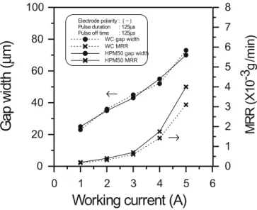
The main objective of EDAD of mold material is to generate a front spark gap between the electrode and workpiece leading grinding function occured precisely. Therefore, it was essential to determine the relationship of gap width to working current. The machining parameters such as the discharge current, break-down voltage, pulse duration, dielectric strength, and electrode polarity have obvious effects on EDM performance. For the sake of simplification, only the discharge current factor was selected to change the front spark gap width, which is the most import-ant factor for EDAD, as will be discussed in Sect. 3.4. Figure 5 shows the effect of varying discharge current on the front spark gap width with an electrolytic copper electrode containing 0 wt.% SiCp. The results indicate that, whether using WC or HPM 50, the front gap width increases as the current increases, and there is little gap difference between the two materials.
Material removal rate is one of the important parameters for evaluating the EDM machining performance for a particular working setup. This rate depends on a large number of properties of the workpiece material, including its melting point, thermal conductivity, and latent heat. It is also influenced by the proper-ties of the electrodes, and by geometric factors such as the shape and dimensions of the electrode and workpiece. Figure 5 also
Fig. 5. Effects of working current on gap width and MRR using a copper electrode for WC and HPM50 as work materials
shows the variation of working current vs. material removal rate. The results also indicate that the MRRs of P20 WC and HPM 50 increase as the current increases.
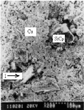
3.2 Effect of electroless copper plating on electrode strength Good bonding status between SiCp and copper can prevent the SiCpfrom peeling off the copper matrix when the grinding func-tion is introduced in the EDAD operafunc-tion. Through the elec-troless plating process, a copper film can be plated on a SiCp surface fully and this copper film will diffuse with the copper matrix during the sintering process. Figure 6 shows the variation of tensile strength vs. SiCp size, demonstrating that the tensile strength of composites using uncoated SiCp is lower than that of composites with electroless copper plated SiCp. SEM mi-crographs of the fracture surface of the composite with 3µm, 20wt.% non-coated SiCpare shown in Fig. 7a, in which arrow 1 indicates the decohesion of the SiCp/Cu interface, and arrow 2 indicates SiCpcracked by pressing or tensile test; all SiCps show relatively flat surfaces of row SiCppowder shape, and these ob-servations depict the poor bonding status for sintered Cu/SiCp without electroless Cu plating pretreatment. The fracture surface of the composite with 3µm, 20 wt.% coated SiCp is shown in Fig. 7b, in which arrow 1 indicates SiCp at the dimple bottom with the appearance of a covering of copper film, and arrows 2 and 3 indicate good bonding status between Cu and SiCp, the copper film on the SiCpsurface is still observed on the fracture surface. In Fig. 7a, the fracture surface shows the presence of de-cohesion at the SiCp/Cu interface. However, the occurrence of the SiCp fracture is observed in Fig. 7b, and this indicates that there was a load transfer from the matrix to the SiCp.
3.3 Observation of the electrical discharge machining and grinding surface
The EDMed surfaces of HPM 50 and P20 using row copper rod, i.e., 0 wt.% SiCp, as an electrode are shown in Fig. 8. It generally
Fig. 6. Effect of particle size on the tensile stress of sintered Cu/SiC com-posite
Fig. 7a,b. SEM micrographs of the fracture surface of: a non-coated electrode, b copper coated electrode
has a complex appearance covered by shallow craters, spheri-cal particles, and pockmarks formed by entrapped gases escaping from the redeposit material on HPM 50 (Fig. 8a). A number of evenly distributed network grain boundaries are identified on the P20 workpiece (Fig. 8b), and pinholes can also be observed on the grain surface, apparently caused by gas bubbles expelled from the molten material during solidification. Typical surface structures of HPM 50 mold steel surface machined by EDAD are shown in Fig. 9. In Fig. 9a, with a 63µm SiCp electrode and 2A working current, the estimated SiCpprotrusion value is
Fig. 8a,b. The typical morphology of an EDMed surface using row copper electrode: a HPM50, b P20
19µm (30% of the SiCpsize) and the average front spark gap is 35µm (obtained from Fig. 5). The former is much smaller than the latter. It seems that the electrical discharge grinding function has little effect on the workpiece surface, for only some shallow grinding traces were observed on the bigger spherical particles surface or higher protrusion of the workpiece.
With a 250µm SiCp electrode and 2A working current, as shown in Fig. 9b, the estimated SiCpprotrusion is 75µm and the front spark gap between the matrix and workpiece is 36µm ap-proximately. The SiCpprotrusion passes through the resolidified
Fig. 9a–d. SEM micrograph showing surface morphology of EDADed that with composite electrode of various SiCpsizes at 2250 rpm rotating speed,
125 ms pulse-on time and 2 A cur-rent setting: a HPM 50, 63µm SiCp,
1 is crater, 2 is spherical particle, 3 is pock mark. b HPM 50, 250µm SiCp, c HPM 50, 150µm SiCp, d P20,
150µm SiCp
zone and penetrates into the heat-affected zone, or possibly even deep into the matrix. Under this EDAD condition, the material removal rate is attributed mainly to the grinding mechanism. Ev-ident proof of the dominant grinding effect can be found from the grinding marks covering the whole EDADed surface, except for some deeper craters caused by the EDM mechanism.
When SiCpsize and working current were optimally selected with a 150µm SiCpelectrode and 2A working current, only the protrusion around the spark crater was ground away from the ma-trix, as shown in Fig. 9c. The total material removal rate under
this EDAD condition is attributed to both the EDM process and the protrusion grinding process.
In Fig. 9d, when 150µm SiCp size and 2A working cur-rent were selected to EDAD P20 WC/Co, the dominant grind-ing mechanisms were still unclarified since both WC and SiCp possess a high melting point (SiCp: 2600◦C, WC: 2720◦C) and high room temperature microhardness (Knoop, SiCp: 2200– 3000 kg mm−2, WC: 1700–2400 kg mm−2) [17]. From the ob-servation of the shallower grinding mark on the EDADed P20 surface, it seems that the WC/Co recast layer can still be ground
by SiCp possibly due to the fact that its hardness is substan-tially higher than that of WC. However, the heat affected zone and matrix of the working piece are too hard to be attacked by Cu/SiCpdrilling.
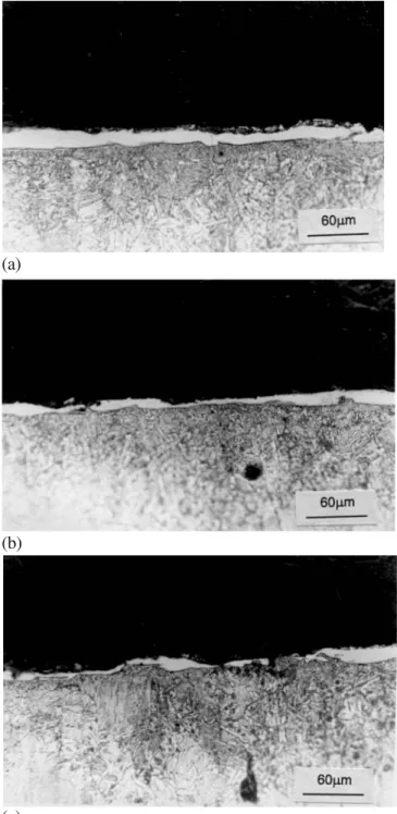
Figure 10 shows the optical micrograph of the cross-section taken from HPM50 specimens after the EDAD operation, in
Fig. 10a–c. Optical micrograph showing the thickness of the white layer of HPM 50 after EDADed with various SiCpsizes electrode at 2250 rpm
rotating speed, 2 A current setting, 125µs pulse-on time: a 63 µm SiCp,
b 150µm SiCp, c 250µm SiCp
which three layers are observed: resolidified layer, heat affected layer, and matrix. When etched with a dilute nitric acid solu-tion, the outmost layer (called white layer) in these specimens remained bright and featureless, i.e., they were nonetchable. This white layer was formed when the outermost molten material was quenched at an extremely high rate by flushes of the dielectric. The optical micrograph of Fig. 10a shows the white layer of the EDADed surface with a 63µm SiCp electrode, and both pock marks and microcracks are observed on this layer and no grind-ing trace is observed in this figure. Figure 10b shows the white layer of specimens with optimum SiCp content and electrode-rotating speed, a thin white layer after grinding action is ob-served, and the ungrounded white layer has the same thickness as that of the white layer in Fig. 10a. Using an electrode with a larger SiCp size, the white layer is pricked, and the heat af-fect zone is ground by SiCpdirectly, and the results are shown clearly in Fig. 10c.
To understand the mechanism of particle size effect on EDAD, it is necessary to examine the relationship between the gap width between the workpiece and electrode, the thickness of the recasted zone and the SiCp size. A schematic illustra-tion of these relaillustra-tionships is presented in Fig. 11, where HPM 50 was adopted for consideration. The white layer thicknesses were measured at various points on different cross sections of the specimen EDADed at the selected current; the width was obtained by measuring the gap from the electrode top surface to the workpiece surface; the SiCp grains’ protrusion height was about 30% of the average SiCp grain size. As can be seen from Fig. 11a, when the working current was set at 1 A, the
Fig. 11a–c. Schematic illustration of the relationships between particle size, gap width and thickness of recasted zone with various currents: a 1 A, b 3 A, c 5 A
gap width between the electrode and workpiece shown in Fig. 5 was 25µm and the recasted zone was 21 µm. The protrusion of the electrode with 63µm SiCp was 19µm, which was al-most in contact with the recasted zone, and the grinding function had little effect on the workpiece surface. The MRR of EDAD were nearly the same as that of EDM, using copper as the elec-trode. The white layer was ground by the particle protrusion of the electrode with 150µm SiCp, and the matrix was ground by the particle protrusion of the electrode with 250µm SiCp. Gap width and recasted zone thickness increased with increasing working current. In Figs. 11b and c, when 3 A and 5 A current were set, the gap width was 43µm and 70 µm, and the aver-age recasted zone thickness was 23µm and 25 µm respectively. Only at the particle protrusion of electrode contacts recasted zone can grinding action occur, i.e., the matrix would be ground at 3 A working current with a 250µm SiCp electrode and only the protrusion was ground when at 3 A working current with a 150µm SiCpelectrode and 5 A working current with a 250µm SiCpelectrode.
The appearance of the EDADed surface (Figs. 9b and c) de-picts that the protrusion and the spherical particles, protruding from the workpiece surface, would be ground first by the pro-truded SiCp. Undoubtedly, the surface roughness of the EDADed surface would therefore be finer than that of the EDMed sur-face. Figure 12 shows that the surface roughness of the HPM 50 EDADed surface using electrodes with 0µm and 3 µm SiCp is higher than that of the electrode with SiCp sizes larger than 63µm, and this is attributed to the electrode grinding function being introduced on the workpiece surface. In addition, the sur-face roughness of the EDADed HPM 50 sursur-face using an elec-trode with 3µm SiCp is higher than that with 0µm SiCp, and this is possibly explained as follows: when at the same work-ing current and workwork-ing area, the electrode with 3µm SiCpcan induce higher current density on a workpiece because some Cu is replaced by SiCp, and this leads to the localized workpiece melting and vaporizing. Deeper craters and higher protrusions are thus induced and this results in higher surface roughness. When applying EDAD P20, the surface roughness increased as the SiCp size of electrode varied from 0µm to 3 µm, possibly
Fig. 12. The surface roughness of an EDADed surface at 2250 rpm rotation speed, 125µs pulse-on time and 2A current setting
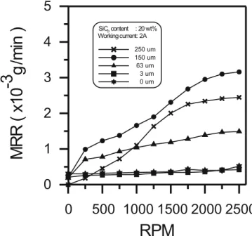
Fig. 13. The effect of electrode rotating speed on MRR of HPM 50 using electrodes with various SiCpsizes
for the same reason as mentioned above. However, the slow decrease of surface roughness with SiCp sizes increasing from 3µm to 250 µm on EDAD P20 could be caused by the fact that the grinding action on WC/Co could not function as effectively as that on WC.
3.4 Effects of electrode rotating speed and working current on MRR
The results in Fig. 13, when HPM 50 is selected as the work-piece, show the effect of electrode rotating speed on MRR with various SiCp size electrodes at 2 A working current. It demon-strates that all of the MRRs of EDAD, when using composite electrodes and at 0 RPM rotating speed, are lower than when using a pure copper electrode; the MRR of EDAD approached zero when the 250µm SiCpelectrode was used. These phenom-ena may be explained as follows: when EDAD is performed with composite electrode, and the electrode and workpiece are moved to a very small gap by servomechanism, only the copper, which possesses low electrical resistance on the electrode front surface, can generate a spark. No sparks were induced from the SiCp to the workpiece because of the high electrical resistance of the SiCp. Consequently, the surface area occupied by Cu metal on the electrode front is the major factor in determining the MRRs by EDM while using the same machining parameters. As the SiCp wt.% increases in the electrode, the area occupied by Cu on the electrode front would be lessened leading to a decreased sparking area and resulting in a lower MRR. For the electrode with 250µm SiCp, the SiCpprotrusions are larger than the spark gap, therefore no spark was generated between electrode and workpiece unless the protruded 250µm SiCp were crushed by moving the EDM machine head forward to form a smaller SiCp protrusion and let a spark be generated. This is the reason why
the MRR of EDAD is near zero when using 250µm SiCp elec-trode at 0 RPM rotating speed.
When EDAD was performed with a copper electrode or 3µm SiCp electrode, the MRR retained a low value, i.e., 0.3 × 10⁻³g/min in this experiment, despite the electrode ro-tating speed being gradually increased. This is attributed to the fact that no grinding action happened between the electrode and workpiece since nil SiCp protrusion could grind the workpiece surface, or the SiCpprotrusions were too short to grind the work-piece surface. The MRRs under this machining condition were dominated by the EDM operation. In comparison with the MRR of the copper electrode, the larger SiCpsize (i.e.,> 3 µm) elec-trodes exhibited far lower MRRs than did the copper electrode. It also can be observed that the MRR of EDAD with a 3µm SiCp electrode is slightly lower than that of the copper electrode. This phenomenon complies well with the EDAD mechanism.
When EDAD uses a 63µm SiCp electrode, the MRR of EDAD increases steadily as electrode rotating speed increases, since the grinding operation is introduced and only the top height of the EDM surface was ground away (as shown in Fig. 9). The MRR increment can be attributed to the fact that more mate-rial was being ground away by the SiCpas the electrode-rotating speed increased. When EDAD uses a 150µm SiCpelectrode, the MRR of EDAD also increases steadily from 0 to the 1250 RPM electrode rotating speed range. The MRR values are higher than that of a 63µm SiCpelectrode, for more SiCpprotrusion enables the attacking of the resolidified layer. However, it is interesting to note that when the electrode rotating speed is over 1250 RPM, the MRR of EDAD increased dramatically and leveled off after 2250 RPM. This is attributed to the fact that under this high rotat-ing speed condition the unsolidified layer had the capability (or the possibility) to encounter the protruded SiCpand was ground away by SiCp, leading to much higher MRR values.
When EDAD with a 250µm SiCp electrode was used, the MRR increased with the higher electrode rotating speed from 0 to 1000 RPM. In this stage, only the grinding function was performed, for the SiCp protrusions were far greater than the spark gap. The MRR was attributed to the grinding action and increased with higher electrode rotating speed. However, in prac-tice, the SiCpprotrusions would be pressed ahead and become smaller after crushing with the workpiece by the EDM machine head’s servo movement; the smaller crushed SiCp would grind the recasted zone. Consequently, the MRR increments are also observed from 1000 RPM to 1750 RPM. When the rotating speed exceeds 1750 RPM, the MRR increments tend to level off. The MRR of EDAD are still lower than that with 150µm SiCp electrode. From the above results, it is suggested that the EDAD process can be achieved only under optimum condition of choos-ing SiCp size, electrode speed and workchoos-ing current.
Figure 14 shows the specific value of MRR, i.e., the ratio of MRR (EDAD) /MRR (EDM), using various SiCpsize electrodes and working currents. When optimum machining parameters are selected (which in the present study are 2250 RPM electrode ro-tating speed, 2 A working current, and 150µm SiCpelectrode), it was found that as high as seven times the normal EDM material removal rate could be achieved in EDAD operation. Allied with
Fig. 14. The specific value of the MRR of EDM and EDAD of HPM 50 at different SiCpand working currents with 2250rpm electrode rotating speed
the expected finer surface roughness in EDAD than the EDM processes (as described in the last paragraph of Sect. 3.3), the EDAD appears a much better processing choice than EDM.
4 Conclusions
The combined functions of electrical discharge abrasive drilling (EDAD) can be soundly realized by using an electrode rotat-ing facility with well-bounded metal matrix composite electrode (Cu/SiCp) made by the powder metallurgy method. The function mechanism is proposed and discussed. Higher material removal rate and lower surface roughness can be achieved when suitable electrode rotating speed, SiCpsize, and working current are cho-sen. Experimental results showed that when using HPM 50 mold steel as the workpiece, the EDAD machining efficiency was three to seven times that of normal EDM operation. The surface rough-ness of P20 and HPM50 could be improved in comparison with that achieved after EDM.
References
1. Llanes L, Idanez E, Martinez E, Casas B, Esteve J (2001) Influence of electrical discharge machining on the sliding contact response of cemented carbides. Int J Refract Metals Hard Mater 19:pp35-40 2. Khairy ABE (1990) Die-sinking by electrosion-dissolution machining.
Ann CIRP 39(1):191–195
3. Trueman CS, Huddleston J (2000) Material removal by spalling during EDM of ceramics. J Eur Ceramic Soc 20:1629–1635
4. McGeough JA, De Silva A, Senbel HA, Lee SC, Wang JY (2001) Wheel dressing and discharge effects in electrochemical grinding of titanium alloy. Proc 13th ISEM CIRP 1:327–337
5. Benedict GF (1987) Non-traditional manufacturing processes. Dekker, New York
6. Lin YC, Yan BH, Chang YS (2000) Machining characteristics of ti-tanium alloy using combination process of EDM with USM. J Mater Process Technol 104:171–177
7. Zhixin J, Jianhua Z, Xing A (1997) Study on a new kind of combined machining technology of ultrasonic machining and electrical discharge machining. Int J Mach Tools Manuf 37(2):193–199
8. Thoe TB, Aspinwall DK, Killey N (1999) Combined ultrasonic and electrical discharge machining of ceramic coated nickel alloy. 92(93):323–328
9. Wansheng Z, Zhenlong W, Shichun D, Guanxin C, Hongyu W (2002) Ultrasonic and electric discharge machining to deep and small hole on titanium alloy. J Mater Process Technol 120:101–108
10. Ya Grodzinskii E (1979) Grinding with electrical activation of the wheel surface. Mach Tooling 50:10–17
11. Vitlin VB (1981) Model of the electrocontact-abrasive cutting process. Sov Eng Res 1(5):88–98
12. Ya Grodzinskii E, Zubotava LS(1982) Electrochemical and electrical-discharge abrasive machining. Sov Eng Res 2(3):90–98
13. Wang X, Ying B, Liu W (1996) EDM dressing of fine grain super abrasive grinding wheel. J Mater Process Technol 62:299–302 14. Snoeys R, Van Dyck F (1972) Plsma channel diameter growth affects
stock removal in EDM. Ann CIRP 21 (1):39–40
15. Matthews FL, Rawlings RD (1993) Composite materials: engineering and science. Chapman Hall, London
16. Koshy P, Jain VK, Lal GK (1996) Mechanism of material removal in electrical discharge diamond grinding. Int J Mach Tools Manuf 36(10):1173–1185
17. Sunniva RK (1989) ASM engineered materials reference book. ASM International, Metals Park, OH