© 2008 WILEY-VCH Verlag GmbH & Co. KGaA, Weinheim
p s s
current topics in solid state physics
c
status
solidi
www.pss-c.com
physica
phys. stat. sol. (c) 5, No 6, 1702– 1705 (2008) / DOI 10.1002/pssc.200778594
Structural and optical properties
of indium-rich InGaN islands
Wen-Che Tsai, Hsuan Lin, Wen-Chen Ke, Wen-Hao Chang*
, Wu-Ching Chou, Wei-Kuo Chen, and Ming-Chih Lee**
Department of Electrophysics, National Chiao Tung University, Hsinchu 300, Taiwan Received 7 September 2007, revised 30 November 2007, accepted 26 December 2007 Published online 17 April 2008
PACS 61.05.cp, 68.37.Ps, 68.65.Hb, 78.55.Cr, 78.67.Hc, 81.15.Gh
* Corresponding author: e-mail [email protected], Phone: +886-3-5712121 ext.56111, Fax: +886-3-5725230 ** e-mail [email protected], Phone: +886-3-5712121 ext.31993, Fax: +886-3-5725230
© 2008 WILEY-VCH Verlag GmbH & Co. KGaA, Weinheim
1 Introduction Ternary InGaN alloys have been an
important active material for nitride based optoelectronic devices [1], particularly for commercial light-emitting di-odes (LEDs) and laser didi-odes operating in the blue-green and ultraviolet spectral ranges [2]. Recently, it has been shown that the energy gap of InN is around 0.7 eV [3, 4], rather than the previously accepted value of 1.9 eV. This finding makes In-rich InGaN alloys become a promising material for applications in the near infrared (NIR) spectral range.
In the last decade, In-rich nanostructures formed by lo-cal compositional fluctuations in InGaN alloys have been intensively investigated, because they were believed to act as “quantum dots” for localizing carriers and were consid-ered to play a key role in the high radiative efficiency of InGaN-based LEDs [5, 6]. InGaN quantum dots formed via self-assembled island growth have also attracted much attention in the past few years [7–10]. However, the InxGa1-xN dots reported to date are still in the Ga-rich side
(x <0.5), with typical emission wavelength in the blue-green range. On the In-rich side (0.5< <x 1), the study of InxGa1-xN dots with NIR emissions is still absent.
Previously, we have demonstrated that InN nanodots can be formed on GaN surface during the initial stage of heteroepitaxial growth using MOCVD. This kind of InN nanodots exhibit intense photoluminescence (PL) emis-sions in the NIR range and show pronounced quantum size effects [11, 12]. In this study, we further investigate In-rich InxGa1-xN islands (with x >0.87) grown by MOCVD at various temperatures. Surface morphologies, alloy compo-sitions and PL emission properties of these In-rich InxGa1-xN islands have been studied by atomic force mi-croscopy (AFM), x-ray diffraction (XRD), PL measure-ments, near-field scanning optical microscopy (NSOM). The influences of growth temperature on island formation, alloy decomposition and their impacts on the optical prop-erties of In-rich InGaN islands are discussed.
2 Experimental The uncapped InGaN islands sam-ples were grown on Sapphire (0001) by MOCVD using trimethylgallium (TMGa), trimethylindium (TMIn), and NH3 as source materials. After nitridation of the substrate at 1120 °C, a thin GaN nucleation layer was first grown at
520 °C, followed by a 2-µm-thick undoped GaN buffer
layer grown at 1120 °C. After the growth of the GaN
Indium-rich InxGa1-xN islands (x ≥0.87) grown by metalor-ganic chemical vapor deposition at growth temperatures rang-ing from 550-750°C were investigated. With the increasing growth temperature, the InGaN dot size increases while the dot density decreases due to the enhanced surface migration of In/Ga adatoms at elevated temperatures. In addition, the composition of InGaN islands was also found to be varied with the growth temperature. At lower growth temperatures, a higher Ga content can be achieved due to the relatively lower
migration ability of Ga adatoms. At higher growth tempera-tures, the deposited InGaN material tend to decompose into In-rich islands and a thin Ga-rich layer. Photoluminescence investigations show that these In-rich islands exhibit a near-infrared emission band. For samples grown at higher tem-peratures, a visible emission band was also observed. The visible emission band may arise from defect bands introduced during the formation of Ga-rich InGaN layer.
phys. stat. sol. (c) 5, No 6 (2008) 1703
www.pss-c.com © 2008 WILEY-VCH Verlag GmbH & Co. KGaA, Weinheim Contributed
Article
buffer layer, the substrate temperature was decreased to
550-750°C to grow InGaN islands using modulated
pre-cursor injection schemes. The prepre-cursor flow rates were 1, 150 and 18,000 SCCM (SCCM denotes cubic centimeter per minute at STP) for the TMGa, TMIn and NH3,
respec-tively. The details of the gas flow sequence have been re-ported in [12]. The only difference is that a 1 SCCM TMGa flow was supplied concurrently with the TMIn flow to grow InGaN alloys. During TMGa and TMIn flow
peri-ods, the NH3 background flow rate was controlled at
10,000 SCCM. PL measurements were carried out at T = 10 K using the 325-nm line of a He-Cd laser as an excita-tion source. The PL signals were analyzed by a 0.5 m monochromator and detected by either a photomultiplier tube or a cooled extended InGaAs detector (with a cutoff wavelength at 2.05 µm) for the visible and NIR spectral ranges, respectively. For NSOM measurements, a fiber tip was mounted on the tuning fork of an AFM system for si-multaneous measurement of the surface morphology and emission signal using the illumination-collection mode. The tip-sample distance was kept at ~30 nm controlled by the shear-force feedback mechanism.
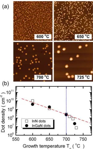
Figure 1 (a) AFM morphology of InGaN islands grown at dif-ferent temperatures. The images shown are in an area of 5×5 µm2. (b) The dot density as function of growth temperature.
3 Results and discussion Figure 1(a) shows the surface morphologies of InGaN islands grown at different growth temperatures ranging from Tg = 600-725 °C. With
the increasing Tg, the average height and diameter of the
InGaN islands increased from 24 to 114 nm and 75 to 410 nm, respectively; whereas the dot density decreased from 4.0×10⁹ to 2.2×107 cm-2. The dot density as function of Tg
is depicted in Fig. 1(b). For Tg = 600-700 °C, the
decreas-ing dot density with the increasdecreas-ing Tg can be attributed to
the enhanced migration length of adatoms, yielding much larger and less dense islands at higher growth temperatures [12]. A rapid decrease in dot density for Tg > 700°C can be
seen and dropped eventually to zero at 750°C. This can be attributed to the desorption of metallic In from the growing surface. We have also prepared a series of samples with InN islands grown at different Tg under similar growth
conditions. The density of InN islands as a function of Tg
was also shown in Fig. 1(b). A similar dependence of dot density on Tg for both InGaN and InN islands can be seen,
implying that the nucleation of InGaN islands is governed by the surface migration of In adatoms, rather than Ga or both.
Figure 2 X-ray diffraction curves (a) and the corresponding In compositions x (b) of the InGaN islands grown at different tem-peratures.
Figure 2(a) shows XRD θ-2θ scans of the InGaN dot samples near the InN(0002) and GaN(0002) diffraction peaks. A diffraction curve of InN film grown on GaN was also included. For the InGaN samples, a broad diffraction peak corresponding to ternary InGaN islands was found to shift gradually toward the InN(0002) as Tg was increased
from 550 to 725°C. For the sample grown at 750°C, the InGaN peak disappeared, due to the complete desorption of In from the growing surface. The corresponding In content (x ) of the InxGa1-xN islands estimated using the Vegard’s
law is depicted in Fig. 2(b). The In content was found to increase from 0.87 to 0.99 as Tg was increased from 550 to
1704 Wen-Che Tsai et al.: Structural and optical properties of indium-rich InGaN
© 2008 WILEY-VCH Verlag GmbH & Co. KGaA, Weinheim www.pss-c.com
physica
p s s
statussolidi
c
lower diffusion ability of Ga adatoms. At lower Tg, the
growth is under the kinetic-dominant condition so Ga in-corporation at island sites could be more dominant. With the increasing Tg, the growth conditions become closer to
the thermodynamic conditions, which allows the Ga ada-toms to select thermodynamically more stable sites and hence hinders the incorporation of Ga adatoms into the In-rich islands. The above mentioned mechanism suggests that the formation of In-rich InGaN islands is very likely to arise from phase separation, rather than SK growth. As can be seen from the case of Tg = 725°C, the InxGa1−xN islands
become highly In-rich, with x up to 0.99. Therefore, it can be inferred that most of the deposited Ga adatoms are very likely to be distributed among these In-rich islands, form-ing a thin Ga-rich layer.
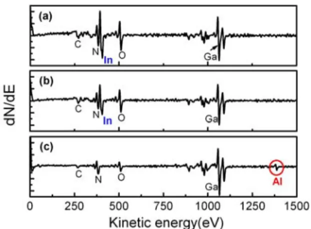
To further confirm this assertion, we have also grown a sample with InGaN islands formed on AlGaN/sapphire
(0001) at 725 °C. The sample was then investigated by
Auger electron spectroscopy (AES) to distinguish the sur-face composition of In, Ga and Al. Fig. 3(a) and 3(b) are the AES results of surface composition measured on In-GaN islands and on flat region without islands, respec-tively. As shown in Fig. 3(c), after 3 min Ar+ sputtering (with the sputtering rate of 3.5 nm/min) on flat region without islands, the indium signal disappeared, while the Al signal emerged, indicating that a thin Ga-rich InGaN layer was formed among these In-rich islands.
Figure 3 AES of InGaN islands grown on AlGaN buffer layer. Surface composition on dot (a), on flat region among islands (b) and on flat region after 3 min. Ar+ sputtering (c).
We would like to point out that the deduced In content from Fig. 2(a) does not follow the prediction of equilib-rium solubility of GaN in InN based on thermodynamic considerations [13], where the Ga content is expected to increase with the growth temperature. For example, in Ref. [6], the solubility of GaN in InN is predicted to be 3% at 550 oC and 6% at 725 oC, while our result shows 13% at 550 oC and about 1% at 725 oC. This implies that the in-corporation of Ga into InN during the growth of InGaN
is-lands is affected by surface kinetics of In and Ga adatoms rather than equilibrium solubility.
PL measurements of these In-rich InGaN islands in both the visible and the NIR ranges are shown in Fig. 4(a) and 4(b), respectively. No PL signal was observed for the 550°C grown sample. Samples grown at Tg = 600-725°C
exhibit a NIR emission band in the range of 0.77-0.92 eV. The redshift in PL peak energy with the increasing Tg
agrees fairly well with the corresponding In content deter-mined by XRD. Therefore, we identify the NIR band as the emission from In-rich InGaN islands. For the sample grown at 750°C, the NIR band disappeared due to the ab-sence of In-rich islands, which is also consistent with its surface morphology and XRD data. Apart from the NIR band, we also observed a visible emission band in the range of 2.0-2.4 eV for samples grown at Tg ≥650°C.
Significantly, the visible emission is even stronger for the sample grown at Tg = 750°C, in spite of the absence of
In-rich islands, implying that the visible band is not originated from the InGaN islands.
Figure 4 Photoluminescence spectra of InGaN grown at differ-ent temperatures from 550 to 750°C in (a) the NIR and (b) the visible spectral ranges.
To further clarify this point, we have performed NSOM measurements at room temperature to obtain both the surface morphology and the spatial distribution of visi-ble emissions. Figure 5(a) shows such a NSOM image of the 725°C sample mapping at its visible emission peak. The corresponding surface morphology is shown in Fig. 5(b). It can be clearly seen that these two images are nearly complementary, with dark spots in the NSOM image cor-respond very well with the In-rich islands revealed in the AFM image. This confirms that the visible emission is in-deed originated from the “flat region” outside these In-rich islands. As can be seen from Fig. 5(a), the visible emission is mainly contributed from some bright spots located a-mong these In-rich islands. As mentioned above, the de-posited Ga atoms during the growth of InGaN islands may form a thin Ga-rich layer among these In-rich islands, due to the considerable shorter migration length for Ga ada-toms. The visible emission band may be originated from
phys. stat. sol. (c) 5, No 6 (2008) 1705
www.pss-c.com © 2008 WILEY-VCH Verlag GmbH & Co. KGaA, Weinheim Contributed
Article
defect centers induced during the formation of the Ga-rich layer.
Figure 5 (a) NSOM image of the 725°C grown sample mapping at its visible emission peak at room temperature. (b)The corre-sponding AFM image.
4 Conclusion In summary, the surface morphologies,
alloy compositions and PL properties of In-rich InGaN is-lands grown by MOCVD at Tg = 550-750°C have been
in-vestigated. The nucleation of InGaN islands was found to be governed by the surface migration of In adatoms. In particular, we found that the incorporation of Ga into InN during the growth of InGaN islands is governed by adatom migration capability, which tends to decompose into In-rich islands and a thin Ga-In-rich layer at higher growth tem-peratures. In-rich islands exhibit PL emission in the NIR range, while the formation of a thin Ga-rich layer is likely to be responsible for the observed visible emission band.
Acknowledgements This work is supported in part by the project of MOE-ATU and the National Science Council of Tai-wan under grant No. NSC M-009-047, NSC M-009-012, NSC M-009-044-MY3, and NSC 95-2112-M-009-020.
References
[1] See for review, Group III Nitride Semiconductor Com-pounds, edited by B. Gil (Clarendon, Oxford, 1998). [2] S. Nakamura and G. Fasol, The Blue Laser Diode (Springer,
Berlin, 1997).
[3] V. Yu. Davydov, A. A. Klochikhin, R. P. Seisyan, V. V. Emtsev, S. V. Ivanov, F. Bechstedt, J. Furthmüller, H. Ha-rima, A. V. Mudryi, J. Aderhold, O. Semchinova, and J. Graul, phys. stat. sol. (b) 229, R1 (2002).
[4] J. Wu, W. Walukiewicz, K. M. Yu, J. W. Ager III, E. E. Haller, H. Lu, W. J. Schaff, Y. Saito, and Y. Nanishi, Appl. Phys. Lett. 80, 3967 (2002).
[5] S. Nakamura, Science 281, 956 (1998).
[6] K. P. O’Donnell, R. W. Martin, and P. G. Middleton, Phys. Rev. Lett. 82, 237 (1999).
[7] H. Hirayama, S. Tanaka, P. Ramvall, and Y. Aoyagi, Appl. Phys. Lett. 72, 1736 (1998).
[8] K. Tachibana, T. Someya, and Y. Arakawa, Appl. Phys. Lett. 74, 383 (1999).
[9] B. Damilano, N. Grandjean, S. Dalmasso, and J. Massies, Appl. Phys. Lett. 75, 3751 (1999).
[10] C. Adelmann, J. Simon, G. Feuillet, N. T. Pelekanos, B. Daudin, and G. Fishman, Appl. Phys. Lett. 76, 1570 (2000). [11] W. C. Ke, C. P. Fu, C. Y. Chen, L. Lee, C. S. Ku, W. C.
Chou, W.-H. Chang, M. C. Lee, W. K. Chen, W. J. Lin, and Y. C. Cheng, Appl. Phys. Lett. 88, 191913 (2006).
[12] W. C. Ke, L. Lee, C. Y. Chen, W. C. Tsai, W.-H. Chang, W. C. Chou, M. C. Lee, W. K. Chen, W. J. Lin, and Y. C. Cheng, Appl. Phys. Lett. 89, 263117 (2006).
[13] I. Ho and G. B. Stringfellow, Appl. Phys. Lett. 69, 2701 (1996).