行政院國家科學委員會專題研究計畫 成果報告
白光 ZnO 螢光體合成與效率提昇及其於電激與場放射平面
光源之應用研究
研究成果報告(精簡版)
計 畫 類 別 : 個別型 計 畫 編 號 : NSC 97-2221-E-151-005- 執 行 期 間 : 97 年 08 月 01 日至 98 年 07 月 31 日 執 行 單 位 : 國立高雄應用科技大學電子工程系 計 畫 主 持 人 : 楊素華 計畫參與人員: 碩士班研究生-兼任助理人員:蔡政勳 碩士班研究生-兼任助理人員:王千鴻 碩士班研究生-兼任助理人員:陳家興 碩士班研究生-兼任助理人員:黃士峰 碩士班研究生-兼任助理人員:黃顯弼 報 告 附 件 : 出席國際會議研究心得報告及發表論文 處 理 方 式 : 本計畫涉及專利或其他智慧財產權,1 年後可公開查詢中 華 民 國 98 年 10 月 23 日
行政院國家科學委員會補助專題研究計畫
成 果 報 告
□期中進度報告
白光 ZnO 螢光體合成與效率提昇及其於電激與場放射平面光
源之應用研究
計畫類別: 個別型計畫
□ 整合型計畫
計畫編號:NSC
97-2221-E-151-005
執行期間:97 年 8 月 1 日
至 98 年 7 月 31 日
計畫主持人: 楊素華
共同主持人:
計畫參與人員: 蔡政勳,王千鴻,陳家興,黃士峰
成果報告類型(依經費核定清單規定繳交):精簡報告 □完整報告
本成果報告包括以下應繳交之附件:
□赴國外出差或研習心得報告一份
□赴大陸地區出差或研習心得報告一份
出席國際學術會議心得報告及發表之論文各一份
□國際合作研究計畫國外研究報告書一份
處理方式:除產學合作研究計畫、提升產業技術及人才培育研究計畫、
列管計畫及下列情形者外,得立即公開查詢
□涉及專利或其他智慧財產權,一年□二年後可公開查詢
執行單位:國立高雄應用科技大學
白光 ZnO 螢光體合成與效率提昇及其於電激與場放射平面光源之應用研究
楊素華 陳家興 蔡政勳 王千鴻 黃士峰 國立高雄應用科技大學 高雄市 807 建工路 415 號 Tel: +886-7-3814526-5631 Fax: +886-7-3811182 中文摘要 本實驗藉由固態燒結法合成白光氧化鋅螢光粉。為達到白光放射,實驗所使用的活化 劑包括銪、釔、鎢、鎵、鈰、及鎵,催化劑則為鋰及鉀化學元素。首先我們改變活化劑的 材料種類,接著再改變活化劑的摻雜濃度。藉由結晶特性及光激光譜儀分析得知最佳摻雜 種類及濃度後,隨後改變其燒結溫度,燒結時間及催化劑的摻雜,以評估不同燒結溫度, 時間的長短及催化劑添加對螢光粉特性所造成的影響。所得到之螢光粉利用研磨機再加以 研磨,經由改變研磨頻率及時間,以得到顆粒較細小之螢光粉,並分析不同研磨條件對螢 光粉顆粒表面型態及結構對發光特性的影響。至於研磨後之熱處裡條件也是本研究的探討 重點。從實驗結果可知合成參數影響螢光粉之發光波長及強度。將最佳條件下所製作之螢 光粉製作成螢光面並應用於場放射元件及電激發光元件。螢光薄膜及場放射元件和電激發 光元件之發光特性已加以量測及討論並有多篇論文發表於國內外研討會及期刊;申請中之 專利一件。 ABSTRACTIn this study, white-light ZnO based phosphor was synthesized by solid-state reaction method. The activators were europium (Eu), yttrium (Y), tungsten (W), gallium (Ga), cerium (Ce), gallium (Ga), and the fluxes were lithium (Li) and potassium (K) elements. The doping concentrations of activators and fluxes were varied to find the optimum doping concentration, meanwhile, the sintering temperature and sintering time were optimized. In addition, the synthesized phosphor was ground with different time and frequencies to obtain fine particles of phosphor. From the measurements, it shows that the luminescence properties of ZnO phosphors were strongly influenced by the synthesis conditions. The field emission display (FED) and electroluminescence device (ELD) were prepared with the optimized characteristics of phosphor. The luminescence properties of phosphor film, FED and ELD were measured and discussed. The characteristics of white-light ZnO based phosphor were presented in several symposiums and published in the journals; a patent is applied and is under examined.
INTRODUCTION
Luminescence is the emission of light generated by low temperatures. It is different from incandescence occurring at high temperatures. It can be emitted by photoluminescence, cathodoluminescence, electroluminescence, thermoluminescence, chemiluminescence, bioluminescence, and triboluminescence. Luminescence is also a process in which the molecule in the excite state relaxes to the ground state by radiation to release energy [1-3]. The radiation process can be divided into fluorescence and phosphorescence by the decay time. The different between fluorescenceand phosphorescenceisthatthefluorescencedoesn’tinvolvethechangeof the spin. The life time of the fluorescence is 10-9~ 10-5s and the life time of the phosphorescence is 10 -4 ~ 10 s. The reason of the short lifetime for fluorescence is that the S1→S0transition is dipole-allowed, and the long lifetime of phosphorescence is because of the low probability of T1→S0transition [4,5]. The luminescence property of the phosphor is dependent on the elements,
purity of the material and the temperature, including concentration quenching, thermal quenching and poisoning [6,7].
ZnO is a direct band-gap Ⅱ-VI semiconductor material having the energy gap of 3.37 eV at room temperature with high exciton binding energy (60 meV) [8-10]. ZnO is unique host material for doping of optically active impurities and luminescence centers which exhibit efficient luminescence even at room temperature [11]. ZnO generally emits a strong UV luminescence band around 370 nm ascribed to band edge emission and several other visible bands in the blue, green and yellow wavelengths resulting from defect emission. The defects in ZnO film include oxygen vacancy (Vo), zinc vacancy (VZn), interstitial zinc (Zni), interstitial oxygen (Oi) and anti-site oxygen (OZn). According to the report, the energy level caused by the interstitial ions of Zn is -50 meV. In the case of oxygen vacancy, the energy levels are located at -40 meV and -190 meV from the conduction band edge. In the case of Zn vacancy, it is placed at -2.5 eV from the conduction band edge [12-13].
ZnO phosphor has been extensively applied as an efficient phosphor for vacuum fluorescent display devices, plasma display panel (PDP), FEDs, and ELDs because it has high efficiency at low-voltage operation, outstanding stability and relatively high electrical conductivity as compared to conventional sulfide phosphor materials [14-15].
The rare-earth elements have been widely used in optoelectronic devices due to its particular optical characteristic for the 4fn electron configuration, for example 4fn5s25p6 for Xe [16-17]. With the variation of n value the transition form and energy level are different. The light of the most trivalent rare-earth are come from the transition between the 4f inner configurations and the f electrons are sheltered from the 5s25p6electrons, so the spectrum line will not be influenced by the surround environment and the characteristics of the f-f energy level transition are: the emission spectrum is narrower and is slightly affected by the temperature; the emission spectrum is insensitive to the environment; the concentration quenching effect is insignificant; the temperature quenching effect is decreased; and the range of the spectrum distributes from UV to IR region. However, some rare-earth ions, for example Ce3+, Tb3+, Pr3+, Eu3+, Sm2+ and Yb2+, which have the energy level transition of 4f-5d, the absorption and emission spectra are dependent on the surround environment. The characteristics are: the absorption and emission spectra are wide; the emission spectrum isn’teasy affected by theenvironment; the temperature will influence the emission spectrum; and the range of the spectrum distributes from UV to IR regions [18-20].
In this study, white-light ZnO phosphor was synthesized by solid-state reaction method and doped with different activators and flux [21]. The synthesis conditions were optimized and the grinding process Addition, the synthesized phosphor was ground with different time and frequencies to obtain fine particles of phosphor. From the measurements, it shows that the luminescence properties of ZnO phosphors were strongly influenced by the synthesis conditions. The field emission display (FED) and electroluminescence device (ELD) were prepared with the optimized characteristics of phosphor. The luminescence properties of phosphor film, FED and ELD were measured and discussed.
EXPERIMENTS
We used the solid-state sintering method to synthesize the phosphor powder of zinc oxide (ZnO); different dopants were doped. First, we mixed the powders of ZnO (99.999%) and dopants with different doping concentrations. After that, powders were mixed with DI water, and then milled the solution for 24 hours in a ball mill machine. The solution was dried in an oven, and ground the dried powders subsequently. The ground powders were sintered at different sintering temperatures for different sintering time. Finally, the obtained powders were ground and the ZnO-base phosphor powders were obtained. The redox reaction was proceeded during the high temperature sintering process.
A Philips XL-40 field emission scanning electron microscope (SEM) system operating at 10 kV was used to find the surface morphology of the ZnO phosphors. The energy dispersive X-ray
analysis (EDX) was used to analyze the chemical characterization of phosphor. X-ray diffraction (XRD) is a measurement technique used to identify the crystalline property of materials. The JEOL, JAMP-9500F Auger electron spectroscopy with a Mg Kαphoton source of 500 W and the binding energy (BE) ranging from 0 to 1100 eV, was used for XPS measurement of the sample. The Hitachi F-7000 fluorescence spectrophotometer with a 150 W xenon lamp and a monochrometer was used to measure the PL spectra and PLE spectra of phosphor under room temperature. The commission internationale del′Eclairage(CIE) coordinates and luminescence properties of devices were measured by Konica Minolta CS-100A colorimeter.
RESULTS AND DISCUSSION
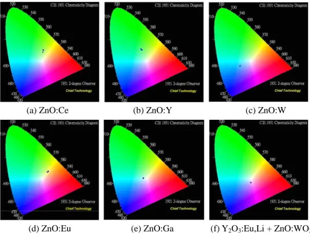
Figure 1(a) shows the ZnO:Ce phosphor prepared with 2 mol% Ce doping concentration, which was sintered at 1000℃ for 8 hours.Its CIE coordinates is located at (0.38, 0.42). It shows that this is a yellow-green phosphor. Figure 1(b) shows the ZnO:Y phosphor prepared with 3 mol% Y doping concentration, which was sintered at 1300℃for 8 hours; its CIE coordinates was located at (0.29, 0.45), was a green phosphor. And Fig. 1(c) shows the CIE coordinates of the ZnO:WO3, where the doping concentration of WO3 was 50 mol% and the sintering temperature was at 1100℃. The CIE coordinates were much closed to (0.24, 0.29). Fig. 1(d) shows the CIE coordinates for the ZnO:Eu2O3phosphor prepared with 3 mol% of Eu doping, which was sintered at 950℃for4 hours. Its CIE coordinates is located at (0.41, 0.41), was a yellow phosphor. Figure 1(e) shows the CIE coordinates of ZnO:Ga2O3 phosphor. It is observed that when the Ga doping concentration 4 mol%, the near white light emission phosphors could be acquired; the CIE coordinates were (0.32, 0.34). From the measurements of CIE coordinates, it was found that the ZnO-based phosphors was not a pure white emission; the maximum emission intensity was obtained from the ZnO:WO3. Hence, complementary phosphor was adopted to achieve white-light emission. Figure 1(f) shows the CIE coordinates of Y2O3:Eu,Li mixed with ZnO:WO3 phosphor. The Li-doped Y2O3:Eu2O3 phosphor was doped with 11 mol% of Eu dopant and 20
FIG. 1. CIE coordinates of phosphors, (a) ZnO:Ce, (b) ZnO:Y, (c) ZnO:W, (d) ZnO:Eu, (e)
ZnO:Ga, and (f) Y2O3:Eu,Li mixed ZnO:WO3.
(a) ZnO:Ce (b) ZnO:Y (c) ZnO:W
Mol% of Li dopant. The phosphors could exhibit a near white light emission. Its CIE coordinates when it was excited by a 6W UV lamp.
From Fig. 1, it was found: 1. The ZnO:WO3 of ZnO based phosphors could achieved white-light emission when it was mixed with complementary phosphor of Y2O3:Eu,Li. 2. The luminance of phosphor could be enhanced by doping with fluxes. 3. The maximum luminance of ZnO:W could be obtained when the mole ratio of ZnO to WO3was 1:1, that is, the synthesized phosphor was ZnWO4. In order to obtain high luminance of white-light emission, the luminance of had to be improved. Hence, the luminance of ZnWO4phosphor was enhanced by doping with fluxes and grinding to obtained fine particle of phosphor.
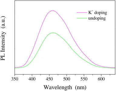
Figure 2 shows the XRD patterns of K+-doped ZnWO4phosphor with different KCl doping concentrations, where the concentration of WO3 was 50 mol%. It shows that the crystallinity of K+-doped ZnWO4 phosphor could be improved by increasing the doping concentration of KCl [15]. From the SEM images of K+-doped ZnWO4 phosphor, it shows that the grain size was increased by KCl doping; it was about 10 to 20 μm. In addition, the PL spectra of K+-doped ZnWO4 phosphor shows that the maximum blue luminescence was obtained when the doping concentration of KCl was 7 mol%. The emission of phosphor, both in the UV and visible regions, was enhanced by KCl doping. If the doping concentration of KCl was above 7 mol%, the concentration quench effect would be occurred. It shows that there just Zn, O, W and K elements exist on K+-doped ZnWO4 phosphors. EDX analyses of ZnWO4 phosphor displays that the concentration of Zn was decreased with the doping of potassium.
20 30 40 50 60 70 2 mol% In te n si ty (a .u .) (4 2 0 ) (2 0 2 ) (0 2 2 ) (4 0 0 ) (2 2 1 ) (2 2 0 ) (0 2 1 ) (2 0 0 ) (0 2 0 ) 2 (degree) 5 mol% 7 mol% 10 mol%
FIG. 2. XRD patterns of K+-doped ZnWO4phosphor with different KCl doping concentrations.
+
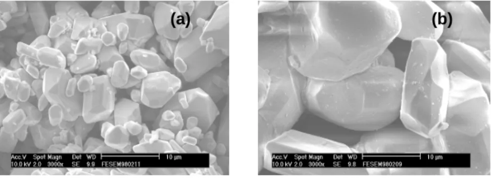
The XRD patterns of the K+-doped ZnWO4 phosphor showed that the crystallinity of phosphor did not change significantly when the temperature was increased. The peaks (200) and (220) were enhanced as the temperature was increased. The SEM images of the K+-doped ZnWO4 phosphor prepared at 700 and 900℃ are shown in Fig. 3. The particle size of phosphor was increased with the sintering temperature, and it was about 2-10 μm. The PL measurements of the K+-doped ZnWO4 phosphor with different sintering temperatures showed that the highest luminous intensity was obtained when it was synthesized at 900℃. The luminescence was increased 30%, when the doping concentration of KCl was 7 mol%, as shown in Fig. 4.
350 400 450 500 550 600 K+doping undoping P L In te n si ty (a .u .)
Wavelength (nm)
FIG. 4. PL properties of the ZnWO4phosphor without and with 7 mol% K+doping.
In order to prepare fine particle of K+-doped ZnWO4 phosphor, the phosphor powder was ground. It was observed that a high grinding frequency (≧15 Hz) led to severe surface crack of the phosphor. When the grinding frequency was above 25 Hz, the particle of phosphor was broken. The PL spectra of the K+-doping ZnWO4 phosphor show that when the grinding frequency increased, the luminous intensity was increased. Nevertheless, when the grinding frequency was above 20 Hz, structural damage of the phosphor resulted in a decreased PL intensity. It was found that the luminance of the phosphor after grinding was increased around 10.97, 16.53, 21.13, 25.36 and 3.62% when the grinding frequency was increased from 5 to 25 Hz. The luminance intensity was declined because of immoderate grinding at high frequency of 20 Hz.
The SEM images of the K+-doped ZnWO4 phosphor prepared with grinding frequency at 20 Hz. It is observed that when the grinding time was increased, the particle of phosphor was cracked. A clear rift was observed when it was ground for 2 minutes, and the particle was broken when the grinding time was over 3 minutes. Structural damage of the phosphor particle led to a reduced luminescence when the grinding time was over 2 minutes. The luminescence was enhanced around 9.63%, 25.36% and 3.08% as the phosphor was ground for 1, 2 3 min, respectively. When the phosphor was ground over 3 minutes, over grinding led to structural damage, consequently, the luminescence was decreased significantly. Figure 5 shows the PL spectra of the K+-doped ZnWO4phosphor with and without grinding; the grinding frequency was set at 20 Hz and the phosphor was ground for 1 min.
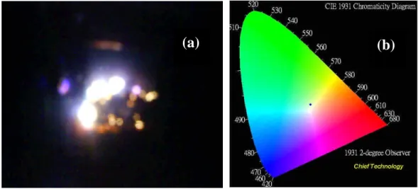
In this study, the white-light ZnO based phosphors on FED and ELD applications were carried out. The white-light phosphor was consisted of K+-doped ZnWO4, the ZnO based phosphor, and the complementary phosphor of Y2O3:Eu,Li. Figure 6(a) shows the performance image of FED in which the field emitters were ZnO nanorods and the white-light phosphor screen was made of mixed phosphor by screen printing. The emission area of FED was 2×2 cm2. When
the applied voltage of field emitters was at 940 V, the luminance of FED was 155 cd/m2. The CIE coordinates of this FED was shown in Fig. 6(b). Figure 7 shows the relationship of current and voltage for the white-light FED. The threshold voltage was about 370 V when the emission current was 1 μA.
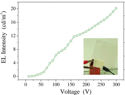
For the preparation of white-light ELD, the structure of ITO/phosphor/insulator/metal was fabricated. This phosphor and insulator films were prepared by screen printing, and the metal electrode was prepared by screen printing and evaporation. The thicknesses of phosphor and insulator were about 8 and 10 μm, respectively. The materials of insulator and metal were BaTiO3 and Ag, respectively. However, the luminance of white-light ELD was low and the applied voltage was high, as shown in Fig. 8, where the operation frequency was set at 1 kHz. To achieve high luminance white-light ELD, the structure of ELD and the properties of phosphor have to be modified further. These are under studied.
350 400 450 500 550 600 P L In te n si ty (a .u .) ungrinding grinding
Wavelength (nm)
FIG. 5. PL spectra of the K+-doped ZnWO4 phosphor with and without grinding; the phosphor was ground at 20 Hz for 1 min.
FIG. 6. (a) The performance image and (b) the CIE coordinate of white-light FED. The emission
area of FED was 2×2 cm2.
FIG. 7. Relationship of current and voltage for the white-light FED.
FIG. 8. Relationship of luminance and voltage for the white-light ELD.
CONCLUSIONS
For the preparation of white-light ZnO based phosphors, it was found that white-light phosphor was obtained from the ZnWO4, the emission color could be improved by complementing with phosphor of Y2O3:Eu,Li. In the mean time, the addition of KCl flux enhanced the luminance of phosphor. When the fine particles of phosphor were obtained by grinding, a higher luminance was achieved. The optimal grinding parameters were frequency at 20 Hz and ground for 1 min.
The findings of this study about the fabrication of field emitters were presented in the NANO KOREA 2008 The 6TH INTERNATIONAL NANOTECH SYMPOSIUM &
0 200 400 600 800 1000 1200 0.0 4.0x10⁻⁶ 8.0x10⁻⁶ 1.2x10⁻⁵ 1.6x10⁻⁵ C u rr en t (A ) Voltage (V) 0 50 100 150 200 250 300 0 4 8 12 16 20
E
L
In
te
n
si
ty
(c
d
/m
2)
Voltage (V)
EXHIBITION; the paper NO. was PTM002, and the title of this paper was “characterization of Ag-catalyzed ZnO nanostructure prepared by vapor-solid mechanism.”This presented paper was accepted for publication in the CURRENT APPLIED PHYSICS, 9 (2009) e180-e184. Meanwhile, the paper about the synthesis and characteristics of white-light ZnO based phosphor, ZnWO4, was published in the JOURNAL OF SOLID STATE ELECTROCHEM, DOI 10.1007/s10008-009-0884-4. Moreover, a patent of this study is applied and it is under examined, the application No. is 097132711. In addition, the reports of newly findings are under written and they will be submitted to the journals for publication soon. Although the emission characteristics of white-light ZnO based phosphor on ELD application have to be improved, the investigations of this study are useful to us for the next study.
JOURNAL PAPER
1. Su-Hua Yang, Fu-Shou Tsai, Jia-Xing Chen, “Characterizations of white-light ZnWO4 phosphor prepared by blending complementary phosphor”, Journal of Solid State
Electrochemistry,DOI 10.1007/s10008-009-0884-4, June 2009.
2. Su-Hua Yang, Pao-Chih Chen, Sheng-Yu Hong, “Characterizations of Ag-catalyzed ZnO Nanostructures Prepared by Vapor-Solid Mechanism”, Current Applied Physics”, 9, e180-e184, 2009.
CONFERENCE PAPER
1. Su-Hua Yang, Pao-Chih Chen, Sheng-Yu Hong, “Characterization of Ag-catalyzed ZnO nanostructure prepared by vapor-solid mechanism”, The 6th International Nanotech Symposoum & Exhibition, Seoul, Korea, Aug. 27-29, 2008.
2. S. H. Yang, P. C. Chen, S. Y. Hong, and C. H. Tsai, “Synthesis and field emission characterizations of Ag-catalyzed ZnO nanostructure”, The 40th Anniversary of International Conference on Solid State Devices and Materials (SSDM), Tsukuba, Japan, September, 24-26, 2008.
3. Sheng-Yu Hong, Su-Hua Yang, Cheng-Hsun Tsai, “Structural, electrical, and optical properties of indium-doped zinc oxide nanoballs by vapor-phase transport”, 2008 International Electron Devices and Materials Symposia (IEDMS), Taichung, November 28-29, 2008.
4. Fu-Shou Tsai, Jia-Xing Chen, Su-Hua Yang, “Preparation and photoluminescence characterizations of white ZnO:Ga3+ phosphor”, 2008 International Electron Devices and Materials Symposia (IEDMS), Taichung, November 28-29, 2008.
5. Cheng-Hsun Tsai, Su-Hua Yang, “Structural, electrical, and optical properties of gallium-doped zinc oxide nanostructures prepared by vapor-phase transport”, International Conference on Optics and Photonics in Taiwan (OPT’08), Taipei, December 4-6, 2008. 6. S. H. Yang (楊素華 ), F. S. Tsai (蔡傅守), J. X. Chen (陳家興), “Preparation and
characterizations of white-light Y2O3:Eu,Li blended ZnWO4 phosphor”,Annual Meeting of the Physical Society of Republic of China, Changhua, January 19-21, 2009.
7. Cheng-Hsun Tsai, Shuo-Xun Li, Su-Hua Yang, “Synthesis and Characterization of Ga-doped ZnO Nanostructures with Different Oxygen Flow Rates”, Int’l Display Manufacturing Conference/3D System and Applications/Asia Display 2009, Taipei, Taiwan, April 27-30, 2009.
PATENT
REFERENCES
[1] M. Liu, X. Q. Wei, Z, G. Zhang, G. Sun, C. S. Chen, H. Z. Zhaung, B. Y. Man, Appl. Surf. Sci., 252 (2006) 4321.
[2] K. Vanheusden, W. L. Warren, C. H. Seager, D. R. Tallant, J. A. Voigt, B. E. Gnade, Appl. Phys. Lett., 79 (1996) 7983.
[3] L. V. Azaroff, Introduction to Solid, McGraw-Hill, (1960) 371.
[4] S. A. M. Lima, F. A. Sigoli, M. R. Davolos, M. J. Jr, J. Alloys Compd., 344 (2002) 280. [5] A. Ishizumi, Y. Kanemitsu, Appl. Phys. Lett., 86 (2005) 253106.
[6] U. N. Maiti, P. K. Ghosh, S. Nandy, K. K. Chattopadhyay, Physica B, 387 (2007) 103. [7] Y. S. Yu, G. Y. Kim, B. H. Min, S. C. Kim, J. Eur. Ceram. Soc., 24 (2004) 1865.
[8] T. H. Zheng, Z, Q. Li, J. K. Chen, K, Shen, K. F. Sun, Appl. Surf. Sci., 252 (2006) 8482. [9] K. Vanheusden, C. H. Seager, W. L. Warren, D. R. Tallant, J. A. Voigt, Appl. Phys. Lett., 68
(1996) 403.
[10] L. Lim, K. Shin, H. W. Kim, C. Lee, J. Lumin., 109 (2004) 181.
[11] S. Q. Zhao, Y. L. Zhou, K. Zhao, Z, Liu, P. Han, S. F. Wamg, W. F. Xiang, Z. H. Chen, H. B. Lu, B. L. Cheng, G. H. Yang, Physica B, 373 (2006) 154.
[12] D. Li, H. Haneda, N. Ohashi, N. Saito, S. Hishita, Thin Solid Films, 486 (2005) 20.
[13] Z. Sosianil, B. Derkowska, P. Dalasinski, Z. Lukasiak, K. B.artkiewicz, W. Bala, M. Addou, A. L. Mehdi, L. Dghughi, I. V. Kityk, B. Sahraouil, ICTON 267 (2005) Th.A2.8.
[14] Y. K. Park, J. I. Han, M. G. Kwak, H. Yang, S. H. Ju, W. S. Cho, J. Lumin., 78 (1998) 87. [15] C. Panatarani, I. W. Lenggoro, K. Okuyama, J. Phys. Chem. Solids, 65 (2004) 1843. [16] C. Q. Ge, C. S. Xie, S. Z. Cai, Mater. Sci. Eng. B, 137 (2007) 53.
[17] R. Kaur, A. V. Singh, R. M. Mehra, J. Non-Cryst. Solids, 352 (2006) 2335.
[18] S. Y. Gao, H. G. Zhang, R. P. Deng, X. M. Wang, D. H. Sun,G. L. Zheng, Appl. Phys. Lett.,
89 (2006) 123125.
[19] P. Che, J. Meng, L. Guo, J. Lumin., 122-123 (2007) 168.
[20] P. L. Chen, X. Y. Ma, D. R. Yang, J. Alloys Compd., 431 (2007) 317. [21] R. L. Coble, J. Appl. Phys., 32 (1961) 787.
出席國際學術會議心得報告
計畫編號NSC
97-2221-E-151-005
計畫名稱 白光 ZnO 螢光體合成與效率提昇及其於電激與場放射平面光源之應用研究 出國人員姓名 服務機關及職稱 楊素華 國立高雄應用科技大學電子系 教授 會議時間地點 2008 年 8 月 27-29 日,Seoul Korea會議名稱 NANO KOREA 2008 The 6
TH
INTERNATIONAL NANOTECH SYMPOSIUM & EXHIBITION
發表論文題目 Characterization of Ag-catalyzed ZnO nanostructure prepared by vapor-solid mechanism
一、參加會議經過
NANO KOREA 2008 The 6THINTERNATIONAL NANOTECH SYMPOSIUM & EXHIBITION
是在 2008 年 8 月 27-29 日於 Seoul Korea 之韓國國際展覽中心 KINTEX 舉行。Conference chair 是 Jo-Won Lee 教授。參加此次研討會之學者專家超過 500 人。NANO KOREA 2008研討會的
議題主要針對為奈米元件之材料、技術、製程、與應用,共七大議題,包括:1. Nano electronics。
2. Nano materials。 3. Nano tools & manufacturing。 4. Nanotechnology for ecology & foods。 5.
Nano Medicine。 6. Energy Nanomaterials。 7. Nano analysis & computational modeling。另外, 大會議規劃了一 Public session-public lectures、一 Special session-EHS (Environment, Health &
safety) 及一 R & BD Seminar。
韓國國際展覽中心 KINTEX,是位於 Goyang West Ilsan 區。KINTEX 是一三層樓的建築,
佔地 224800 m2,非常的廣闊。KINTEX 緊鄰的是 Ilsan central road,Chungagno,和 Han River。
KINTEX 不管是在建築造型的設計,展覽場的規劃,停車場的設置,餐飲服務及周邊公園的 規劃均相當周全。KINTEX 是在 2005 年 4 月 29 日開放使用,曾經幾辦過大型的 2005 Seoul
Motor Show 及多次的展覽會及研討會。KINTEX 共有 5 個展覽館,兩個大型會議廳,一個大 舞廳。KINTEX 與機場的交通非常方便,並有 Seoul Subway 與各大城市連接。NANO KOREA
2008的研討會場是在 KINTEX 的二樓,而展示場及 poster session 是設置於 KINTEX 之第四
R & BD Seminar 是一以商業為主項之研討會。R & BD R & BD 代表的是 Reearch & Business Development,它的意義是表示在韓國所有的活動都與研究和商業有關。R & BD
Seminar 包含兩個 Session;其一是 Technology Transfer Session,另一個 Session 是 Product & Technology Promotion。Technology Transfer Session 對研究協會或大學實驗室的研究人員是非 常有重的。會中的講者會以他們的專利、證照、及 knowhow 當交易。聽眾或參與者多是企業 家或製造商。至於 Product & Technology Promotion Session,任何人想要以為奈米技術當商業
行為者,均可以在會中發表他們的商業模型或是產品。所有 NANO KOREA 參展商都可以參 加此二 Session;每一位講者可以有 20 分中的發表時間。 二、 與會心得 NANO KOREA 2008研討會提供了所有與會的學者專家一起討論和提升與奈米技術相關 領域之基本物理、發展和應用的機會。微奈米技術是全 21 世紀公認的創新技術。對奈米技術 在 energy innovation 方面,與會的學者專家發表了多篇相當實用的論文,特別是在省能及減 少溫室效應的議題上;發表的論文主要是集中 nanostructured reaction-sintered silicon carbide
and joining technology , Deodorization and/or disinfection system using photocatalyst , Thermoelectric generating system using unutilized energy , Nanocomposite polymer for
electric-insulation , Nanocoating technoilogy of EB-PVD , Laser peening technology for strengthening materials through nanoscale abrasion,和 Nondestructive nanosensing technology
using X-ray color image intensifier。
在量子物理方面, quantum dot lasers 的進展,應用及對 silicon photonics 之衝擊性,吸引
了多位的與會者聽講,尤其在 spin-polarized laser 的技術及在 secure communication 之應用引 起熱烈的回響。而在 molecular dynamics simulation,發表者利用 3-D 模擬提供了薄膜成長時
原子級的成長現象,surface intermixing 和 surface structure 於高能離子衝擊時的行為利用 3-D 模擬可以得到深刻的了解。此外在奈米技術於 FPD 之應用亦引起熱烈的注意;譬如奈米 inkjet
printing,nano imprint,和 roll-to-roll 製程技術等。在此議題上,in-line 製程、精準技術、測 量系統、及製成最佳化都有詳細的解說。至於奈米結構、奈米線、奈米管的材料與製程技術
nano flash memory、Theragnostic MR molecular imaging agent、Centrifugal microfluidics、 Photovoltaic technology、nanotechnology in food science、Nanoscale patterning in optical data
storage、Printable electronics、及 nanobiosensor 等議題也受到與會者的熱烈參與。Polymer 奈 米結構及製程,如 hydrophobic polymers 中之 linear low-density polyethylene (LLDPE),亦受到
關注。
NANO KOREA 2008的研討會主要的目的是藉由奈米技術研討會以增加國際學者之互相
討論的機會,對奈米技術之最新研究與發現有所了解,並對此相關領域之發展有所貢獻。為 了加速奈米技術之發展,是有必要整合全世界於半導體工程、光工程,和光設計工程之技術,
而此次研討會正提供了這樣的機會。
在 NANO KOREA 2008 The 6TH INTERNATIONAL NANOTECH SYMPOSIUM &
EXHIBITION研討會,我們發表的論文為“Characterization of Ag-catalyzed ZnO nanostructure
prepared by vapor-solid mechanism”。在此篇論文,我們主要討論了於 Si 基板上成長 ZnO 奈 米線之成長機構及其場放射特性。基板的溫度及觸媒的沉積對 ZnO 奈米線的結構具有決定性 的影響力。三種不同 ZnO 奈米結構,whisker nanorods,protuding film,及 Aligned nanorods,
之 vapor-solid 成長機制在論文及發表會中均有詳細解說。參與NANO KOREA 2008的研討會, 除了從此會中獲得寶貴的知識之外,對於主辦單位籌辦研討會的用心,規劃的創意,參與者
的熱烈迴響,及展覽場的佈置,均讓我印象深刻。會中服務人員的專業及親切的態度亦讓我 感受很深。非常感謝國科會給予出席國際研討會的經費補助。
於NANO KOREA 2008 NANO KOREA 2008研討會所發表之論文如下頁所示。本研究論文
已在該會下之 Current Applied Physics 期刊發表,期刊資料為: Su-Hua Yang, Pao-Chih Chen,
Sheng-Yu Hong, “Characterizations of Ag-catalyzed ZnO Nanostructures Prepared by Vapor-Solid