Polymer Light-Emitting Diode Defect Inspection System
Chia-Ming Chiang (江嘉明), Chiou-Shann Fuh (傅楸善)
Department of Computer Science and Information Engineering,
National Taiwan University, Taipei, Taiwan, R.O.C.
Tel: (02)2362-5336 ext. 327, e-mail: [email protected]
Abstract
This paper has two parts: 1. low-resolution defect inspection, 2. high-resolution defect inspection. In low-resolution defect inspection, we use CCD (Charge-Coupled Device) camera to inspection defective blocks of PLED (Polymer Light-Emitting Diode) panels and replace photometer to measure luminance. In high resolution, we use CCD camera and high-resolution lens to grab image and detect defects based on computer vision and image processing. The experimental result shows that our inspection system achieves high accuracy and high speed for industry and meets our requirement.
1. Introduction
PLEDs work similarly as LEDs, which are semiconductor devices that emit visible light when electric current flows through them, except they have different materials. PLEDs use organic materials to produce and emit the light, but LEDs use semiconductor materials.
Our PLED defect inspection system has two parts. One is low-resolution defect inspection system, and the other is high-resolution defect inspection.
In low-resolution defect inspection, we use the Minolta CS-100 photometer to calibrate our CCD camera in order to measure the luminance that PLEDs emit.
In high-resolution defect inspection, we have to detect defects as precise as 10 micrometers. In the inspection process, we first select a golden image and set up parameters which depend on our requirement,
defects.
This paper is organized as follows. Section 1 gives introduction to how PLEDs work and PLED defect inspection system structure. Section 2 describes some theoretical background that we need to know for our inspection systems. Sections 3 and 4 explain the inspection methods and processes of our low-resolution and high-resolution inspection systems, respectively. Section 5 concludes our methods of PLED inspection systems.
2. Background and Algorithm
Our PLED defect inspection system is based on computer vision and digital image processing and this section describes the background and some algorithms.
2.1. Automatic Binarization
Because we need to segment bright blocks from PLED panels automatically, we use the minimizing within-group variance method [2] to segment images. The method introduced here is based on the minimizing within-group variance method. We can use variance to measure group homogeneity. A group with high homogeneity will have low variance. A group with low homogeneity will have high variance. Therefore, we choose a threshold that minimizes the weighted sum of group variance.
2.2. Pattern Matching
In order to detect defects of interest and register images, we have to find subimages of interest. Therefore, we use the correlation approach [1] to match patterns.
Image Comparison is a simple method to detect defects easily and quickly. First, we need a golden image (image without defect) to serve as a reference. We can compare the inspected image with the golden image pixel by pixel to gain a residual image. Setting a proper threshold to binarize the residual image, we can detect defects from the residual image.
2.4. Projection
Projection [2] is an easy edge detection method when the objects of interest are aligned along one image edge. Projection can be horizontal, vertical, or at any direction. In our PLED defect inspection system, we use horizontal projection and vertical projection to segment each block in an inspected image.
2.5. Gamma Correction
Because we use CCD camera to replace photometer to measure luminance that PLEDs emit, we have to consider whether our CCD camera need to do gamma correction. The gray value of every pixel in an image is generally not proportional to the light that CCD sensor absorbs. Generally speaking, when output signal generated by a physical device has power-law response to input signal, the value of the exponent in the power-law equation is referred to as gamma. Gamma correction is the process to correct the power-law response phenomena [1][4]. The power-law equation has the basic form
γ
cr
s
=
where
c
andγ
are positive constants,s
is output signal, andc
is input signal. For example, CRT (Cathode Ray Tube) devices have an intensity-to-voltage response that a power-law equation hasγ
varying from 1.8 to 2.5. We do some experiments to decide whether our CCD camera has gamma correction problem.3. Low-Resolution Defect Inspection
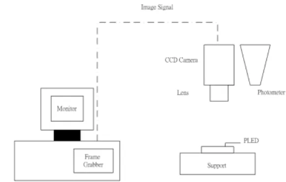
The inspection framework of our
low-resolution defect inspection system is shown in Figure 1. Our system consists of CCD camera, lens, frame grabber, photometer, fixture, and personal computer. In our system, we use monochrome CCD camera to capture PLED images that we want to inspect and analyze and use frame grabber to grab images from CCD camera and store in our computer.
In order to calibrate our CCD camera so that we can use the CCD camera to measure luminance, we use the photometer to do some experiments and calibrate the CCD camera. The fixture can supply PLED with power which PLED needs to illuminate. It also generates five signal patterns so that PLED can generate five patterns.
Because PLEDs are self-illuminant, we do not need any light source. On the contrary, in our inspection process we isolate ambient light from our inspection system so that we can measure luminance exactly. In this inspection system we fix the CCD camera and the fixture. When the fixture generates five signal patterns respectively, the CCD camera captures pattern images one by one.
Figure 1 The framework of low-resolution defect inspection system.
3.1. Classification of Defects
In the low-resolution defect inspection system, we classify defects into macro-defects and micro-defects. Detailed defects are illustrated in Figure 2. Shrinking block means bright blocks shrink and erroneous block means bright block which should not emit light in some patterns, but they emit light. Defect of unevenly bright panel which means whole blocks emit light unevenly.
3.2. CCD camera calibration
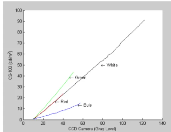
In order to use CCD camera to replace photometer so that we can measure luminance, we do some experiments to calibrate our CCD camera and see whether we have to do gamma correction in this CCD camera or not. First, we have to check the relation between gray level that frame grabber
captures and luminance that CCD sensor absorbs. Our experiment set-up is shown in Figure 3. We use LCD (Liquid Crystal Display) monitor, CCD camera, and Minolta CS-100 photometer. The experiment we do is in a dark room. Except the light that the LCD monitor emits, no light is in a dark room. The LCD monitor emits white, red, green, and blue light respectively. Each channel of light that the LCD monitor emits also has different intensities. To begin with, the intensity of light is the lowest. We gradually increase the intensity of light. In each light intensity, we compute the average gray level of the image that CCD camera captures and use the photometer to measure luminance that LCD monitor emits.
The relation between gray level and luminance is illustrated in Figure 4. We can find that gray level is proportional to luminance. Hence, this shows that our camera does not need gamma correction.
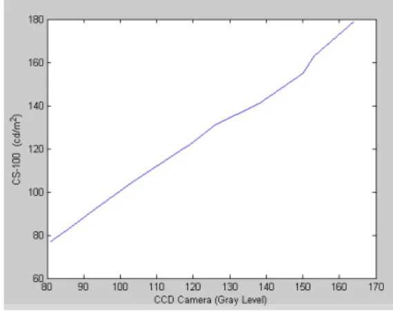
How do we use CCD camera to replace photometer? We replace LCD monitor with PLED panel and tune voltage of PLED panel so that PLED panel emits various luminance. We use CS-100 to measure luminance and also compute average gray level that CCD camera captures. The result is shown in Figure 5. We build a table storing the relationship of luminance and gray level. When we inspect PLED panels, we compute the average gray level of image captured by CCD camera, and then use the average
Figure 2 Classification of low-resolution defects.
Figure 3 Calibration structure.
gray level to check the table to find the corresponding luminance. If the average gray level does not exactly conform to the gray level stored in the table, we use interpolation to find the corresponding luminance.
3.2. Low-Resolution Defect Analysis
In the low-resolution defect inspection system, we have to inspect abnormal bright blocks. The judgment criterion of defect is shown as follows: 1. If the luminance of bright block is more than
luminance upper bound we set up previously then we determine it as excessively bright block. 2. If the luminance of bright block is less than
luminance lower bound we set up previously then we classify the defect into three classes:
i. If the area percentage whose
luminance is less than luminance lower bound is less than the area percentage of insufficient bright block then we determine it as insufficiently bright block.
ii. If the area percentage whose luminance is less than luminance lower bound is less than the area percentage of shrinking block then determine it as shrinking bright block.
iii. If the area percentage whose
luminance is less than luminance lower bound is more than the area percentage of shrinking block then we determine it as dark block. The process of defect detection is shown as follows: Step 1: Use automatic binarization to segment an image and get the size of PLED panel.
Step 2: If the panel size is larger than the tolerance of standard panel size, we mark the panel as size defect. Step 3: Divide the panel image whose size is 590 (w)
×
189 (h) pixels into 61 (w)×
14 (h) blocks. Each block is about 9 (w)×
13 (h) pixels.Step 4: Evaluate the centroids of blocks, and store centroids of blocks into an array.
Step 5: Expand 4 pixels from the centroid of block to left and to right respectively. Expand up and down 5 pixels from the centroid of block respectively. Each block is 9 (w)
×
11 (h) pixels.Step 6: Calculate average gray level of each block, and use the table we build from CCD camera calibration process to transform average gray level to luminance.
Step 7: Use the judgment criterion of defect we define previously to detect defects.
The defective signs are shown in Figure 6. We mark excessively bright blocks as orange, dark blocks green, shrinking blocks blue, insufficiently bright blocks red, and erroneous blocks yellow.
Excessively
bright block Dark block Shrinking block Insufficiently bright block Erroneous block
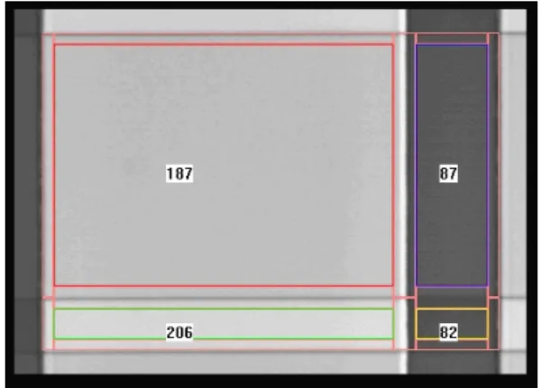
Figure 7 shows that excessively bright column and dark block are inspected. Figure 8 shows that excessively bright blocks are inspected. Figure 9 shows that erroneous blocks, excessively bright blocks, and dark blocks are inspected. Figure 10 shows that the PLED panel is excessively bright. Figure 11 show that insufficiently bright blocks and
Figure 5 The relation between gray level and luminance that PLED panel generates.
shrinking blocks are inspected.
4. High-Resolution Defect Inspection
The inspection framework of our high-resolution defect inspection system is shown in Figure 12.
CCD Camera
Inspection Route
In the system, we fix the CCD camera and send to the CNC X-Y-
θ
table control signals which trigger the CNC X-Y-θ
table to move so that we can capture each block in PLED panels. Figure 13 shows the PLED block inspection sequence.Because we use the telecentric, coaxial, and high-resolution lens and the PLED is not self-illuminant, we need a light source. We use
Figure 7 Inspection result.
Figure 8 Inspection result.
Figure 9 Inspection result.
Figure 10 Inspection result.
Figure 11 Inspection result.
Figure 12 The framework of high-resolution defect inspection system.
coaxial light to illuminate PLED panels.
4.1. Image Segmentation
In the high-resolution inspection system, inspected images may have different sizes. Besides, it is hard to use a single threshold to binarize images to get defects. We have to divide a block into several sub-blocks. For each sub-block, we select a threshold to binarize to detect defects. In this section, we propose a method to segment images automatically. Let P(x) be projection.
We define two means,
>= >= =
∑
0 ) ( | ) ( # 0 ) ( | ) ( 1 dx x dP dx x dP dx x dP dx x dP M x and < < =∑
0 ) ( | ) ( # 0 ) ( | ) ( 2 dx x dP dx x dP dx x dP dx x dP M x .We also define two standard deviations, 1
σ = a standard deviation for all ( )>=0 dx
x dP
and 2
σ = a standard deviation for all ( )<0
dx x
dP .
The edge-finding algorithm is explained as follows: Step 1: Take vertical and horizontal projections of an image to get projection values.
Step 2: Operate low-pass filter on vertical and horizontal projections.
Step 3: Perform the first-order derivative on vertical and horizontal projections.
Step 4: Evaluate
M
1,M
2,σ
1, andσ
2. Use these values to find the ranges whose projection values are above 1.5~1.7 standard deviations.Step 5: We can find edge positions whose projection values are the largest from these ranges.
4.2. Image Inspection and Defect Analysis
We divide a block into 16 sub-blocks and group
these sub-blocks into two classes, edge blocks which cover an edge and flat blocks which do not cover any edge. Figure 14 shows sub-blocks which we divide into. Figure 15 shows sub-blocks classification.
Edge Block Defect Inspection
We propose a method for edge block defect inspection. Edge blocks have two kinds of edges, vertical edge and horizontal edge. For example, edge block 1 has a vertical edge and edge block 4 has a horizontal edge. In the following, we illustrate the method for edge blocks which have a horizontal edge.
Step 1: We sum up columns in an edge block. Evaluate column average.
Step 2: Compare each column with column average pixel by pixel to gain a residual column for each column.
Step 3: Using the threshold we set up previously to binarize each residual column, we can detect defects from the residual column.
For edge blocks which have a vertical edge, we replace column with row instead.
High-Resolution Defect Analysis
We have to inspect defects whose widths or heights are as small as 10 micrometers. Moreover, the resolution of the lens we used achieves 1 pixel equal to 2.136 micrometer. We define the defect bounding box width as w and height as h. The judgment criterion of defect is according to the following:
If (w > 4 pixels and h > 2 pixels), or (w > 2 pixel and h > 4 pixel), we determine the defect as the fatal defect. Otherwise, we determine the defect as the non-fatal defect.
For all fatal defects we mark them as red color. The process of defect detection is shown as follows: Step 1: Use the alignment we develop to align CCD camera and CNC X-Y-
θ
table and get how many micrometers a pixel is equal to.Step 2: Grab a golden image from a non-defect block of PLED to get parameters such as block width, block height, and so on. Besides, we set up parameters such as gray level tolerance, blocks size tolerance.
Step 3: Segment the block to group sub-blocks into edge blocks and flat blocks to get sub-block sizes and sub-block average gray levels. If one of the block sizes of edge blocks or flat blocks is more than our set tolerance, determine it as size defect, compare the block with the golden block pixel by pixel, and go to Step 5.
Step 4: For flat blocks, compare every pixel with its average gray level. If it is more than our set tolerance, mark it as defect pixel. For edge blocks, use the method we develop above to detect defect pixels. Step 5: Perform the connected component labeling on those defect pixels to get bounding boxes of defects. Use the judgment criterion of defect to get fatal defect and mark it as red color.
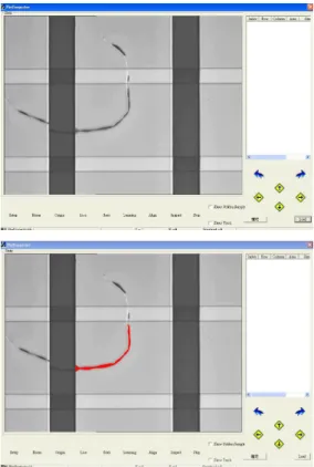
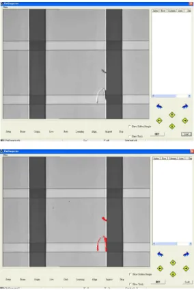
Figures 17 and 18 show that defects in edge neighborhoods are easily detected.
Figure 15 Sub-blocks classification.
Figure 16 Compare each column with column average pixel by pixel to get a residual column for each column.
Figure 17 Inspected image (upper) and inspection result (lower).
5. Conclusions
In this paper, we develop two kinds of PLED defect inspection systems, the low-resolution defect inspection system and the high-resolution defect inspection system.
In the low-resolution defect inspection system, we use CCD camera to replace photometer so that we can measure luminance quickly. The judgment criterion is based on luminance. We previously set up luminance range. Therefore, if the luminance we get from inspection does not meet our requirement, we classify it as defect. In the low-resolution defect inspection system, we can inspect PLED panels quickly and robustly.
In the high-resolution defect inspection system, we can inspect PLED panels quickly and robustly and can detect defect size as small as 10 micrometers.
For edge blocks, the method we develop based on image comparison can detect defects easily.
REFERENCES
[1] R. C. Gonzalez and R. E. Woods, Digital Image
Processing, Addison Wesley, Reading, MA, 2002.
[2] R. M. Haralick and L. G.. Shapiro, Computer
and Robot Vision, Vol. 1, Addison Wesley, Reading,
MA, 1992.
[3] R. M. Haralick and L. G.. Shapiro, Computer
and Robot Vision, Vol. 2, Addison Wesley, Reading,
MA, 1992.
[4] G. C. Holst, CCD Arrays, Cameras, and
Displays, SPIE Press, Bellingham, Washington, 1998.
Figure 18 Inspected image (upper) and inspection result (lower).