國 立 交 通 大 學
光 電 工 程 研 究 所
碩 士 論 文
氮化鎵垂直共振腔面射型雷射
之電流侷限研究
Study of Current Confinement in GaN-based
Vertical-Cavity Surface Emitting Lasers
研
研
究
究
生
生
:
:
陳
陳
政
政
宏
宏
..指
指
導
導
教
教
授
授
:
:
郭
郭
浩
浩
中
中
教
教
授
授
盧
盧
廷
廷
昌
昌
教
教
授
授
中
中
華
華
民
民
國
國
九
九
十
十
九
九
年
年
七
七
月
月
氮化鎵垂直共振腔面射型雷射之電流局限之研究
Study of current confinement in GaN-based vertical cavity
surface emitting lasers
研 究 生:陳政宏 Student:Cheng-Hung Chen
指導教授:郭浩中 Advisors:Hao-Chung Kuo
盧
盧
廷
廷
昌
昌
Tien-Chang Lu
國 立 交 通 大 學
光 電 工 程 研
究 所
碩 士 論 文
A ThesisSubmitted to Institute of Electro-optical Engineering College of Electrical Engineering and Computer Science
National Chiao Tung University in partial Fulfillment of the Requirements
for the Degree of Master in Electro-Optical Engineering
July 2010
Hsinchu, Taiwan, Republic of China
i
摘要
本篇論文旨在製作電激發氮化鎵垂直型共振腔雷射結構搭配混合式布拉格 反射鏡中,透過減薄 ITO 透明導電層的厚度藉此降低光共振在此結構中的內部 損耗,以及在量子井上成長氮化鋁做為電流阻擋層取代原來在 p 型氮化鎵上的 氮化矽,並且量測其電性及光性作進一步的探討。 首先,我們利用模擬的方式計算出 30nm 的 ITO 透明導電層可以有效的降低 內部損耗又可以有效的符合電激發元件所需的電流擴散層效果。此外,本結構 也成功製作於電激發氮化鎵垂直型共振腔面射型雷射中。在室溫下,其雷射的 臨界操作電流為 9.7mA,起始電壓為 4.3V,具有約 180 歐姆的低電阻。在不同 的電流注入下,雷射的頻譜具有單一雷射波長為 412nm,雷射半高寬為 0.5nm。 雷射行為也從自激發發光輻射轉變為受激發發光輻射。自激發光耦合因子及雷 射發散角分別為 5*10-3及 8 度左右。 為了更進一步能夠降低閥值電流並將注入電流作有效利用,我們使用了相較於 氮化鎵高能隙的氮化鋁(6.2eV)成長在量子井上方,如此的設計可以使電流完全注 入量子井內不會因為擴散而造成損失。另外,為了更進一步將共振腔的光學損耗 降低,我們設計了環型的透明導電層取代原先的圓型透明導電層,讓共振光不被 透明導電層所吸收。 透過量測共振腔中的 Q 值,原先以圓形透明導電層的共 振腔 Q 值約為 650 而以環型透明導電之元件 Q 值提升至 1100,與計算結果接近. 在本論文中,我們設計出了室溫電激發面射型雷射並且量測雷射現象,進一步 為了提高雷射的效能我們提出將電流做更有效利用的新結構,並且也可提升共振 腔的品質因子,這樣的設計對於降低閥值電流於電激發元件上是更有效的方法。ii
Abstract
We have investigated the electrical and optical performance in GaN-based VCSELs, which take AlN as current blocking layer and conventional type take SiNx as current layer. We have reported the demonstration of the CW laser action on GaN-based vertical cavity surface emitting lasers (VCSEL) at room temperature. The laser has a threshold current of about 9.7 mA corresponding to the current density of about 12.4 kA/cm2 and a turn-on voltage about 4.3 V at 300K. The lasing wavelength was 412 nm with a linewidth of about 0.5 nm. A spontaneous emission coupling efficiency factor of about 5×10⁻³ and the degree of polarization of about 55% were measured, respectively. The laser beam has a narrow divergence angle of about 8o.
To further decrease the threshold current and optimum the VCSEL structure, we used AlN re-growth on the multiple quantum wells as current blocking layer and optical confined layer. On the other hand, in order to reduce the optical loss in the resonate cavity we take the ring shape ITO to replace the circular ITO layer as usual, through measured the Q factor in the conventional VCSEL the AlN VCSEL, the latter device shows a higher Q factor about 1100 than the conventional 600. It represents that the cavity without ITO layer has a better optical resonate characteristic.
In this report, we demonstrated RT CW lasing VCSEL and also measured the laser characteristics, further more we designed a method to make more efficient in injection current and enhance the quality factor of cavity. Such a technique could be the more ideally structure for reduce threshold current in electrically injected GaN-based VCSEL.
iii
致謝
又是鳳凰花開的時日,這兩年,要感謝的人實在太多太多,不是簡
單的三言兩語可以感謝。 首先,要感謝王老師在每次報告中都和我
們熱烈的討論,並且給予我們更廣闊的思考空間,郭老師總在我們實
驗低潮的時候適時的給予我們鼓勵,尤其在最後最徬徨無助的時候。
最後是盧老師,謝謝老師不厭其煩的和我們討論實驗細節及給予意見,
有實驗室的三位大家長的照顧讓我在這兩年學到的不只是學識並且
做事更有條理謹慎。直屬學長,宗鼎、士偉、博孝,謝謝你們總在我
需要幫忙時伸出援手。明華、博閔、鏡學、李博,有你們強大的磊晶
支援,才讓這篇論文能夠誕生,尤其博閔學長,謝謝你在百忙之中的
高效率幫忙,讓實驗流程能夠更順利! 清華學長,沒有架子的學長,
總是在實驗上給我最有效的建議。
我的好同學們,嗡嗡、阿菲、小昕、重卿、JO、大為、祥奇、阿吉…
這兩年謝謝你們一路的陪伴,讓這兩年更有回憶,我們要出去打拼了,
但千萬別忘記我們所擁有的一切甘苦回憶… 直屬的昀霖,VCSEL 的
棒子終於接下去了,經過一年的共患難,相信你的表現一定能青出於
藍。
iv
在學習的這條路上,特別感謝二姨和五姨,有你們的照顧與關心
讓政宏在這一路上走的很安穩順利。姿蓉,謝謝你這一路的陪伴,忍
受我的脾氣和我一起成長,我們還有很長的路要一起前進。最後,要
感謝我的父母,無怨無悔的付出、給予我最大的關心與支持,希望能
讓你們以我為榮。
2010/07/28 政宏
v
Contents
Abstract (in Chinese)...i
Abstract (in English)...ii
Acknowledgement……….iii
Contents...v
Figure Contents……….………..vii
Chapter 1 Introduction 1.1 Wide band gap Ⅲ-Ⅴ materials……….1
1.2 Semiconductor lasers………2
Chapter 2 Operation principle of VCSEL 2.1 Optical characteristics of Fabry-Perot Resonator cavity 2.1.1 Distributed Bragg reflectors………....8
2.1.2 Quality Factor……….11
2.1.3 Transverse Mode………,,,12
2.2 Electrical characteristics of VCSELs 2.2.1 Threshold current………13
2.2.2 Output power and quantum efficiency………16
2.2.3 Output Beam Characteristics………..17
Chapter3 Experimental principles and methods 3.1 Four point probe………..18
3.2 Atomic force microscope (AFM)………19
3.3 Photoluminescence spectroscopy (PL)………21
3.4 Electroluminescence spectroscopy (EL)……….22
Chapter 4 Characteristics of electrical pumped GaN-based VCSELs 4.1 Previous work of our group 4.1.1Optical pumped VCSEL ………24
4.1.2 CW lasing of current injected GaN-based VCSEL at 77k…..27 4.2 The design of electrical pumped VCSEL
vi
4.2.1The reflectance and quality factor simulation with different
ITO thickness………...31
4.2.2Design structure of electrical pumped device………..34
4.3 Fabrication process of GaN-based VCSELs………...35
4.4 Characteristics of optically pumped GaN-based VCSELs…………..38
4.5 Characteristics of electrically pumped GaN-based VCSELs………..44
Chapter 5 Characteristics of electrically pumped GaN-based VCSELs with AlN Current Blocking Layer 5.1 Characteristics of AlN………52
5.2 Fabrication of GaN-based VCSELs with AlN current blocking layer process 5.2.1 Initial clean and photolithography technique……….55
5.2.2 Epitaxial flowchart ……….56
5.2.3 Process flowchart………61
5-3 Characteristics of electrically pumped GaN-based VCSELs with AlN current blocking layer 5.3.1 The emission images of AlN VCSEL……….64
5.3.2The I-V curves of AlN blocking layer and conventional VCSEL……….67
5.3.3The optical characteristics of AlN VCSEL………..68
5.4 Summary……….69
Chapter 6 Conclusions………...70
vii
Figure content
Fig 1.1 the band-gap diagram of Ⅱ-Ⅵ and Ⅲ-Ⅴ group semiconductor materials Fig 1.3 the schematic diagram of the VCSELs
Fig 1.4 the schematic diagram of three nitride based VCSELs structures Fig. 2.1 Schematic diagrams of DBRs
Fig. 2.2 transmission pattern of a Fabry-Perot cavity in frequency domain Fig. 3.1 four points probe
Fig 3.2 four point probe in NCTU Nano Facility Center
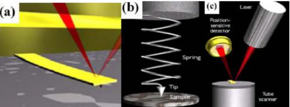
Fig. 3.3 Concept of AFM and the optical lever: (a) a cantilever touching a sample, (b) illustration of the meaning of "spring constant" as applied to cantilevers, (c) the optical lever. Scale drawing; the tube scanner measures 24 mm in diameter, while the cantilever is 100 μm long typically.
Fig. 3.4 The AFM feedback loop. A compensation network monitors the cantilever deflection and keeps it constant by adjusting the height of the sample (or cantilever).
Fig. 3.5 Interband transitions in photoluminescence system
Fig. 3.6 Spectrum of a blue electroluminescent light source. Peak wavelength is at 454 nanometers and the FWHM spectral bandwidth is quite wide at about 9 nm. Fig. 4.1 The schematic diagram of the optical pumped VCSEL structure
Fig. 4.2 PL emission of the optical pumped VCSEL structure. Fig. 4.3 The excitation energy - emission intensity curve (L-I)
Fig. 4.4 The laser emission spectrum with the increasing pumping energy. Fig. 4.5 The schematic diagram of the current injected VCSEL structure Fig. 4.6 Emission spectrum of the current injected VCSEL structure.
viii
Fig.4.7The light output intensity vs injection current and current–voltage characteristics of GaN VCSEL
Fig. 4.8 The laser emission spectrum at different injection current levels measured at 77 K. Figure
Fig. 4.9 The simulation cavity structure
Figure 4.10The simulated reflectance spectra with different thickness of ITO Figure4.11the simulated cavity mode with different thickness of ITO
Figure 4.12 The simulated quality factor with different thickness of ITO
Figure 4.13 Electric field intensity (red line) and refractive index (black line) as a function of the distance from top layer.
Fig 4.14 The schematic diagram of overall VCSELs process flowchart Fib. 4.15 mesa
Fig 4.16 The ITO transparent conduct layer deposited on current aperture Fig 4.17 The schematic diagram of completed electrical pumped VCSEL Fig 4.18 The OM image of completed VCSEL device when current injects Fig 4.19 The schematic diagram of the optical pumped VCSEL structure Fig 4.20 The reflectance spectrum of bottom DBR
Fig. 4.21 The cross section SEM image of VCSEL cavity without upper DBR Fig. 4.22 the PL and reflectance spectrum of VCSEL without upper DBR Fig. 4.23 The reflectance spectrum of upper DBR
Fig. 4.24 The PL spectrum of optical pumped VCSEL with upper DBR Fig. 4.25 The pumping energy density versus normalized intensity diagram Fig. 4.26 The lasing spectrum of optical pumping VCSEL
Fig. 4-27(a)VCSEL full structure (b)turn on image at 2mA
ix
Fig.4-29(a) emission spectra of our GaN-based VCSEL devices at current injection of 0.6 Ith, 1 Ith and 1.2 Ith, respectively (b) the measurement data at different angles and the solid curve is the fitting curve, (insert)the CCD image of a lasing spot size of about 2 m in diameter.(c) the degree of polarization (DOP) of the laser beam
Fig.5.1 (a) AFM of three AlN temperature re-growth conditions Fig.5.1 (b) PL after 2 steps re-growth
Fig.5.1.1 The overall diagram of VCSEL structure Fig.5.2 The reflection spectrum of bottom DBR
Fig.5.3 The cross section SEM image of VCSEL cavity without upper DBR, the insert figure is the thickness of AlN layer.
Fig. 5.4 current aperture defined by SiO2.varying from 3um to 10um Fig. 5.5 The p-GaN surface after liftoff SiO2 and the insert figure point
out the pits on p-GaN
Fig5.6 The PL and reflectance spectrum of VCSEL without upperDBR Fig. 5.7 Mesa etching and turn on image
Fig. 5.8 Passivation step Fig.5.9.1 ring shape ITO Fig. 5.9.2 The ring shape ITO and CCD image
Fig. 5.9 Current lateral spreading by AlN current blocking, the white mark point out the 10um current aperture.
Fig. 5.10 n and p contact Fig. 5.11 upper DBR
Fig. 5.12 Emission images of AlN VCSEL Fig. 5.13 (a) The emission image of
x
(b)(c)(d)Beam-view on 3um aperture emission
Fig.5.14 I-V curve through this ring shape ITO, the VCSEL cavity become a more ideally resonate cavity than conventional VCSEL cavity with an absorption layer ITO.
Fig.5.15AlN VCSEL structure and CCD image of 10um aperture.
1
Chapter 1
Introduction
1.1 Wide-bandgap III-V materials
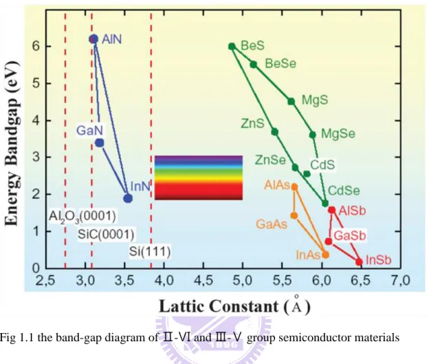
Wide-bandgap nitride materials have attracted great attention over past decade due to their promising potential for the applications of optoelectronic devices such as flat panel display, competing storage technologies, automobiles, general lighting, and biotechnology, and so on [1-4]. The III-N materials are synthesized mainly using the four kinds of atoms, gallium (Ga), nitride (N), aluminum (Al), and indium (In), to form the binary and ternary compounds such as GaN, InN, AlN, InxGa1-xN, and AlxGa1-xN etc. The bandgap of these materials cover a very wide range from 0.9eV to 6.1eV (figure 1.1), which implies the large band off-set in hetero-structure could be achieved in this material system. The large band off-set is very useful to confine carrier for the high-speed and high power electronic devices and light emitting devices [5]. Their wide-range bandgap also provide possibility of full-color emission because they cover red, green, and blue emission regions. This property further makes nitride materials important and important for the applications of full-color display or solid-state lighting. Furthermore, nitride materials still have lots of advantages such as high bond energy (~2.3eV), high saturation velocity (~2.7 × 104 cm/s), high breakdown field (~2 × 10⁶ V/cm), and strong excitonic energy (>50meV)[6-7]. Although wurtzite nitride compounds have some unique properties such as piezoelectric field and spontaneous polarization which is harmful to the efficiency of light emitting devices, the material system still is a very strong candidate for the future optoelectronic applications due to their superior material properties.
2
Fig 1.1 the band-gap diagram of Ⅱ-Ⅵ and Ⅲ-Ⅴ group semiconductor materials
1.2Vertical Surface Emitting Lasers
Although the optimization of the edge emitting laser keeps going, some properties of this kind of laser are unfavorable. One of those properties is its elliptic beam shape. On one hand, the coupling efficiency would be low as the elliptic beam is coupled into optical fiber (typically in the form of circular core). On the other hand, for the application of storage, the elliptic beam not only makes each writing pixel larger but also raises expenses for correcting light shape. Usually, this kind of laser shows slightly large divergence angle to be over ten degree. This also is disadvantageous to the projection. Furthermore, the side emitting laser devices also makes the testing of devices a tough task. The wafer should be cut into several
3
stripes (several laser devices on one strip) before the testing. For a commercial product, the complicated testing would result in a poor producing efficiency and be disadvantageous. Therefore, in order to have a superior laser device, K. Iga [16] demonstrated a new kind of laser diodes, vertical cavity surface emitting laser, in 1977. Vertical cavity surface emitting laser (VCSEL) is a vertical-emitting-type laser. It is formed by sandwiching a few-lambda cavity in a pair of reflectors, usually in the form of distributed Bragg reflector (DBR), with a very high reflectivity (>99.9%) (as shown in figure 1.3). In contrast to EELs, photons in the cavity of VCSEL are vertically in resonance and emit outside perpendicularly to the surface of the structure. This laser diode can have many advantageous properties than conventional edge emitting laser, such as circular beam shape, lower divergence angle, two-dimensional laser array possible, efficient testing, low threshold, and so on. Owing to these superior performances, VCSELs had become very attractive and started to be applied to the commercial products at long wavelength range. In fact, short-wavelength VCSELs are also very promising for the applications of storage, display, and projection. In particular, the use of two-dimensional arrays of blue VCSELs could further reduce the read-out time in high density optical storage and increase the scan speed in high-resolution laser printing technology [17].
4
Fig 1.3 the schematic diagram of the VCSELs
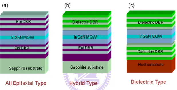
In recent years, several efforts have been devoted to the realization of nitride-based VCSELs [18-27]. Currently, three kinds of structures were reported:
I. Fully epitaxial grown VCSEL structure
In 2005, J. F. Carlin [27]
and E. Feltin [28] demonstrated the wholly epitaxial and high quality nitride-based micro-cavity (as shown in figure 1.4(a)) using metalorganic vapor phase epitaxy (MOVPE or MOCVD). They used the lattice-matched AlInN/GaN as the bottom and top reflectors to avoid cracks happened due to the accumulation of the strain after stacking large pairs of layers. The reflectivity of AlInN/GaN could be achieved as high as 99.4%. They showed the 3/2-lambda cavity emitted a very narrow emission with a linewidth of 0.52 nm, corresponding to a quality factor of ~800.
5
II. VCSEL structure with two dielectric mirrors
Compared to epitaxial grown reflectors, the fabrication of dielectric mirrors is relatively simple. Furthermore, the large index difference of dielectric mirrors makes them could easily have wide stop band (>50nm) and high reflectivity (>99%) by coating just few stacks of 1/4-lambda-thick layers. Therefore, using dielectric mirrors to accomplish nitride-based VCSELs had begun attractive. Song et al. [19], Tawara et al. [20] and J. T. Chu et. al. [22] successively reported the structure (as shown in figure 1.4(c)) after 2000. They employed some process techniques such as wafer bonding and laser lift-off to make dielectric mirrors be coated onto both sides of nitride-based cavity. They showed a micro-cavity could have a very high quality factor to be greater than 400 and achieve lasing action using optical pumping. In addition , Takashi Mukai et al [23] have demonstrated the CW lasing at room temperature in a GaN-based vertical-cavity surface-emitting laser (VCSEL) by current injection in 2008. Its optical cavity consisted of a 7λ-thick GaN semiconductor layer and an indium tin oxide layer for p-contact embedded between two SiO2/Nb2O5 dielectric distributed Bragg reflectors. The threshold current of
VCSEL is 13.9kA/cm2 and the lasing wavelength is about 414nm. However, the fabrication techniques of this kind of VCSEL is relatively complicated, and its cavity length cannot be efficiently controlled due to polishing problems.
III. VCSEL structure with hybrid mirrors
The so-called hybrid mirrors are a combination of two different kinds of reflectors, for example, a dielectric mirror and an epitaxial reflector. Typically, the fabrication of this structure is to grow bottom reflector and cavity using MOCVD and then coat dielectric mirror to complete VCSEL structure (as shown in figure
6
1.4(b)). The hybrid-cavity nitride-based VCSEL\formed by the dielectric mirror and the epitaxially grown high-reflectivity GaN/AlxGa1-xN DBR was reported earlier. In
1999, Someya et al. [18] used 43 pairs of Al0.34Ga0.66N/GaN as the bottom DBR and
reported the lasing action at ~400nm. Then, Zhou et al [21] also employed a bottom DBR of 60 pairs Al0.25Ga0.75N/GaN and observed the lasing action at 383.2nm. Both
these AlGaN/GaN DBR structures required large numbers of pairs due to the relatively low refractive index contrast between AlxGa1-xN and GaN. Therefore, recently some groups began to study the AlN/GaN for application in nitride VCSEL. The DBR structure using AlN/GaN has higher refractive index contrast (Δn/n=0.16)[29] that can achieve high reflectivity with relatively less numbers of pairs. It has wide stop band that can easily align with the active layer emission peak to achieve lasing action. However, the AlN/GaN combination also has relatively large lattice mismatch (~2.4%) and the difference in thermal expansion coefficients between GaN (5.59x10⁻⁶/K) and AlN (4.2x10⁻⁶/K) that tends to cause cracks in the epitaxial film during the growth of the AlN/GaN DBR structure and could result in the reduction of reflectivity and increase in scattering loss. With the mature of epitaxy techniques, the high-reflectivity AlN/GaN DBR structure with relatively smooth surface morphology has become possible with just twenty or thirty pairs [30]. In comparison of these three VCSELs, it doesn’t require complicated process such as laser lift-off technique to complete a hybrid VCSEL device. This means the fabrication of such structure is stable and reliable comparing to other structures. Thus, the hybrid structure is more advantageous in the aspects of fabrication and commercialization In fact, the investigation of the characteristics of the GaN-based VCSELs has gradually attracted more attentions. Kako et al. [31] investigated the coupling efficiency of spontaneous emission (β) and the polarization property of the
7
nitride VCSEL and obtained a high β value of 1.6×10⁻²
and a strong linear polarization of 98%. Tawara et al. [20] also found a high β value of 10-2 in the nitride VCSEL with two dielectric mirrors. Honda et al. reported the estimation of high characteristics temperature of GaN-based VCSEL [32]. These all mean the development of nitride-based VCSEL and the understanding of the laser performance has become more and more important.
8
Chapter 2
Operation principle of VCSEL
2.1 Optical characteristics of Fabry-Perot Resonator Cavity
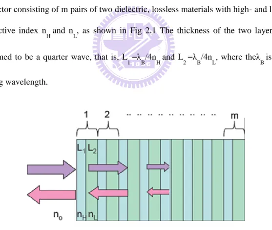
[33-37]2.1.1 Distributed Bragg reflectors (DBR)
DBRs serve as high reflecting mirror in numerous optoelectronic and photonic devices such as VCSEL. There are many methods to analyze and design DBRs, and the matrix method is one of the popular one. The calculations of DBRs are entirely described in many optics books, and the derivation is a little too long to write in this thesis. Hence, we put it in simple to understand DBRs. Consider a distributed Bragg reflector consisting of m pairs of two dielectric, lossless materials with high- and low- refractive index n
H and nL, as shown in Fig 2.1 The thickness of the two layers is
assumed to be a quarter wave, that is, L
1 =λB/4nH and L2 =λB/4nL, where theλB is the
Bragg wavelength.
Figure 2.1 Schematic diagrams of DBRs
9
multiple reflected waves increase the reflectivity with increasing number of pairs. The reflectivity has a maximum at the Bragg wavelength λ
B. The reflectivity of a DBR
with m quarter wave pairs at the Bragg wavelength is given by
where the n
o and ns are the refractive index of incident medium and substrate.
The high-reflectivity or stop band of a DBR depends on the difference in refractive index of the two constituent materials, △ n (n
H-nL). The spectral width of the stop
band is given by
where neff is the effective refractive index of the mirror. It can be calculated by requiring the same optical path length normal to the layers for the DBR and the effective medium. The effective refractive index is then given by
The length of a cavity consisting of two metal mirrors is the physical distance between the two mirrors. For DBRs, the optical wave penetrates into the reflector by one or several quarter-wave pairs. Only a finite number out of the total number of
10
quarter-wave pairs are effective in reflecting the optical wave. The effective number of pairs seen by the wave electric field is given by
~
For very thick DBRs (m→∞) the tanh function approaches unity and one obtains
Also, the penetration depth is given by
where r = (n1-n2)/ (n1+n2) is the amplitude reflection coefficient. For a large number of pairs (m→∞), the penetration depth is given by
Comparison of Eqs. (2.17) and (2.19) yields that
The factor of (1/2) in Eq. (2.20) is due to the fact that meff applies to effective number of periods seen by the electric field whereas Lpen applies to the optical power. The optical power is equal to the square of the electric field and hence it penetrates half as far into the mirror. The effective length of a cavity consisting of two DBRs is thus given by the sum of the thickness of the center region plus the two penetration depths into the DBRs.
11
2.1.2 Quality factor
Since the theory of Fabry-Perot cavity has been explained, we can talk about the finesse and the quality factor of resonant cavity. The cavity finesse, F, is defined as the ratio of the transmittance peak seperation (△ ψ) to the transmittance full-width at half-maximum (δψ):
2
1
1
2
1/2R
R
F
Figure 2.2 shows the transmission pattern of a Fabry-Perot cavity in frequency domain. The finesse of the cavity in the frequency is then given by F = νFSR/△ ν.
Figure 2.2 transmission pattern of a Fabry-Perot cavity in frequency domain
Besides the quality factor Q is also equal to λ/δλ, where δλ is the narrow emission linewidth around λ.
Q
2.1.3 Transverse modeThe nature of the transverse optical confinement determines the possible lateral optical modes that might lase. Although VCSELs tend to lase in only a single axial
12
mode , because the DBR mirrors fill much of the cavity, lateral modes can exist for device diameters down to led than a micro. The losses explicitly discussed above were those of the fundamental lateral mode, although the general discussion may be applied to losses for higher-order modes as well. In fact, the higher-order modes tends to experience higher size-dependent optical losses than the fundamental mode, and this is why it is possible to observe single-mode operation in devices that have diameters of several microns
The transverse mode of gain-guided structures tends to vary with pumping level and thermal environment, and they are rather difficult to analyze analytically. However, the lateral modes of more strongly index-guided VCSELs with etched mesas or graded index dielectric waveguides, provided the Fresnel number is sufficiently large(F~10) so that significant diffraction does not occur in unguided sections. Then, the modes can be determined from normalized dispersion charts, generally used for optical fibers. In both the etched-mesa and dielectrically aperture cases, the effective lateral index profile can be determined by dividing the net change in optical path length over the cavity length by the cavity length. Thus, the assumed uniform waveguide has a lateral index roll-off given by
δ
λ
For a step index resulting from an abrupt dielectric aperture or an etched mesa, the aperture thickness t ( r < a ) = 0 and t ( r > a ) = t. For the etched-mesa VCSEL, t is taken to be if the etch extends just through the top DBR mirror. For a tapered aperture, t ( r ) varies with radius.
The change in the optical path length between the aperture and unapertured regions of the device gives rise to change in the longitudinal resonant wavelength with radius
13
[25]. The shift of the mode due to a change in a physical length, it can be applied general form:
Δλ λδ
Use Eq. (2.26) to determine the effective lateral index step is also possible, though it will not work if the shift becomes large than the longitudinal mode spacing or the mirror stop-band.
2.2
Electrical characteristics of VCSELs
[38]2.2.1 Threshold current
The threshold current Ith of surface-emitting lasers, which is common to semicondu- ctor lasers, in general, can be expressed with threshold current density Jth by the following equation:
where e is the electron charge, and V is the volume of the active region given by
Thus, the threshold carrier density is given by
Here, the parameters used are defined as follows. : Absorption loss coefficient averaged per unit length : Diffraction loss coefficient averaged per unit length
14
: Gain coefficient expressing differential gain ¼ dg/dN with g, optical gain per cm.
: Effective recombination coefficient
d: Total active layer thickness D: Diameter of active region
L: Effective cavity length including spacing layers andpenetration layers of Bragg reflectors
: Transparent carrier density : Photon lifetime in cavity : Recombination lifetime
ξ: Optical energy confinement factor
ξ ξ ξ ξ :Transverse confinement factor
ξ: Longitudinal confinement factor or filling factor relative to stripe lasers
ξ: Injection efficiency, sometimes referred to as internal efficiency ξ : Spontaneous emission efficiency
Parameter
Symbol
Stripe laser
VCSEL
Active layer area S 3 x300 um^2 5 x 5 um^2
Active volume V 60 um^3 0.07 um^3
Cavity length L 300 um 1 um
15 Optical confinement ξ 3% 4% Optical confinement (transverse) ξ 3 –5% 50–80% Optical confinement (longitudinal) ξ 50% 2 x1%x 3 (3QW) Photon lifetime ξ 1ps 1ps Relaxation frequency (low current levels)
<5 GHz >10 GHz
Table I Comparison of dimensions of stripe lasers and VCSELs
As seen from eq. (1), we recognize that it is essential to reduce the volume of the active region in order to decrease the threshold current. Assuming that the threshold carrier density does not change significantly, if we reduce the active volume, we can reduce the threshold until we encounter an increase in diffraction loss and diffusion of carriers. We compare the dimensions of surface-emitting lasers and conventional stripe geometry lasers, as shown in Table I. It is notable that the volume of VCSELs may be V ? 0:06 mm3, whereas that of stripe lasers remains V =60 um^3. This directly reflects the threshold currents in that the typical threshold of stripe lasers has a range of tens of mA or higher, but that for VCSELs can be made less than sub-mA order by a simple carrier confinement scheme such as proton bombardment. It could even be as low as several tens of microamperes by implementing sophisticated carrier and optical confinement structures, as will be introduced later. An early estimation of the threshold showed that the threshold current can be reduced proportionally to the square of the active region diameter. However, there should be a minimum value due to the decrease in the optical confinement factor that is defined
16
by the overlap of the optical mode field and the gain region when the diameter becomes small. In addition, the extreme reduction of volume, in particular, in the lateral direction, is limited by the optical and carrier losses due to optical scattering, diffraction of lightwaves, nonradiative carrier recombination, and other technical imperfections.
2.2.2 Output power and quantum efficiency
We also discuss the differential quantum efficiency of the VCSEL. If we use a nonabsorbing mirror for the front reflector, the differential quantum efficiency d
from the front mirror is expressed, using as
where is the total internal loss (= a + d), and Rf and Rr are front and rear mirror
reflectivities, respectively. The optical power output is expressed by
where Eg is the band-gap energy, C is the spontaneous emission factor, and I is the driving current. On the other hand, the power conversion efficiency P far above the
threshold is given by
where Vb is the bias voltage and the spontaneous component has been neglected. In the case of a surface-emitting laser, the threshold current can be very small, and therefore, the power conversion efficiency can be relatively high, i.e., higher than
17
50%. The power conversion efficiency is sometimes called the wall-plug efficiency.
2.2.3Output Beam Characteristics [34]
In a conventional edge-emitting diode laser, thin epitaxial layers must be used, which has the consequence that the width of optical mode in the direction perpendicular to the layers is always quite small (typically about two free-space wavelength). As a result, the emission angle in that direction is large (often of the order 30o or more). In the direction parallel to the layers, the width of the aperture is usually wider, thus yielding a noncircular beam. As the width of the aperture is widened beyond a few wavelengths, multiple transverse modes are excited and the beam become highly nonsymmetric and not longer diffraction limited. In contrast, a VCSEL with a circular aperture put out a circle beam, which simplifies the coupling into subsequent optical components (e.g., lenses and fibers). Moreover, a VCSEL with a single lateral mode can have an aperture several wavelengths across, thus yielding a narrower output beam than a conventional diode laser.
18
Chapter3
Experimental principles and methods
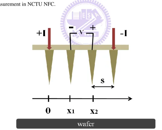
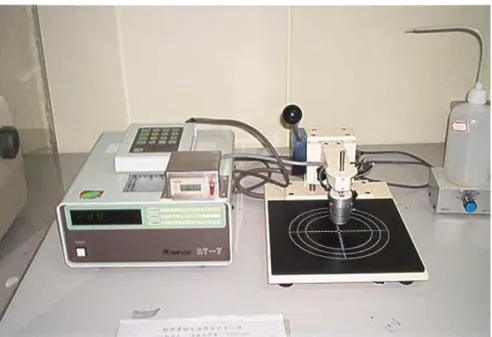
3.1 Four point probe
The 4-point probe setup consists of four equally spaced tungsten metal tips with finite radius. Each tip is supported by springs on the other end to minimize sample damage during probing. The four metal tips are part of an auto-mechanical stage which travels up and down during measurements. A high impedance current source is used to supply current through the outer two probes; a voltmeter measures the voltage across the inner two probes (See Fig3.1) to determine the sample resistivity. Typical probe spacing s ~ 1 mm. Fig 3.2 is the four point probe we used to sheet resistance measurement in NCTU NFC.
Fig. 3.1 four points probe
19
Fig 3.2 four point probe in NCTU Nano Facility Center
3.2 AFM
The atomic force microscope (AFM) or scanning force microscope (SFM) was invented in 1986 by Binnig, Quate and Gerber. Like all other scanning probe microscopes, the AFM utilizes a sharp probe moving over the surface of a sample in a raster scan. In the case of the AFM, the probe is a tip on the end of a cantilever which bends in response to the force between the tip and the sample. The small probe-sample separation (on the order of the instrument's resolution) makes it possible to take measurements over a small area. To acquire an image the microscope raster-scans the probe over the sample while measuring the local property in question.
The resulting image resembles an image on a television screen in that both consist of many rows or lines of information placed one above the other. Unlike traditional microscopes, scanned-probe systems do not use lenses, so the size of the probe rather than diffraction effect generally limits their resolution. As shown in Fig. 3.3. AFM operates by measuring attractive or repulsive forces between a tip and the sample. In its repulsive "contact" mode, the instrument lightly touches a tip at the end of a leaf
20
spring or "cantilever" to the sample. As a raster-scan drags the tip over the sample, some sort of detection apparatus measures the vertical deflection of the cantilever, which indicates the local sample height. Thus, in contact mode the AFM measures hard-sphere repulsion forces between the tip and sample. In tapping mode, the AFM derives topographic images from measurements of attractive forces; the tip does not touch the sample.
The presence of a feedback loop is one of the subtler differences between AFMs and older stylus-based instruments such as record players and stylus profilometers. The AFM not only measures the force on the sample but also regulates it, allowing acquisition of images at very low forces. As shown in Fig. 3.4, the feedback loop consists of the tube scanner that controls the height of the entire sample; the cantilever and optical lever, which measures the local height of the sample; and a feedback circuit that attempts to keep the cantilever deflection constant by adjusting the voltage applied to the scanner. One point of interest: the faster the feedback loop can correct deviations of the cantilever deflection, the faster the AFM can acquire images; therefore, a well-constructed feedback loop is essential to microscope performance. AFM feedback loops tend to have a bandwidth of about 10 kHz, resulting in image acquisition time of about one minute.
21
(b) illustration of the meaning of "spring constant" as applied to cantilevers, (c) the optical lever. Scale drawing; the tube scanner measures 24 mm in diameter, while the cantilever is 100 μm long typically.
Fig. 3.4 The AFM feedback loop. A compensation network monitors the cantilever deflection and keeps it constant by adjusting the height of the sample (or cantilever).
3.3Photoluminescence spectroscopy(PL)
Photoluminescence characterization equipment generally uses the PL method to obtain the wavelength and intensity of the semiconductor material being analyzed. PL is the process of optical absorption of electrons in solids between an initial energy state Ei and a final energy state Ef. Excitation of an electron to Ef will leave Ei
unoccupied creating a hole. Absorption creates electron-hole pairs while luminescence is the process which occurs when electrons in excited states drop to a lower level emitting a photon ħw as shown in Fig. 3.5 The electron–hole recombination creates a photon which is also known as a radiative transition. Direct
22
gap materials are good light emitters and their optical properties are analyzed using this technique.
Fig. 3.5 Interband transitions in photoluminescence system
Photons are absorbed using an excitation source which is typically a laser. The frequency of the source ħwL must be greater than the energy gap Eg. The result is that electrons are injected into the conduction band and holes into the valence band. Electrons and holes are initially created in higher states within these bands but will rapidly relax to the bottom of their respective bands reaching their lowest energy state. Relaxation occurs by emitting phonons, for energy loses from the higher states, which obeys the conservation laws. The difference in energy between the two bands is Eg which is the energy gap, also known as the band gap. Luminescence occurs close to the band gap Eg, near k = 0. After excitation, both electrons and holes relax to their lowest energy states by emitting phonons.
3.4 Electroluminescence spectroscopy (EL)
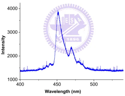
As shown in Fig. 3.6, Electroluminescence (EL) is an optical phenomenon and electrical phenomenon in which a material emits light in response to an electric current passed through it, or to a strong electric field. This is distinct from light
23
emission resulting from heat (incandescence), chemical reaction (chemiluminescence), sound (sonoluminescence), or other mechanical action (mechanoluminescence). Electroluminescence is the result of radiative recombination of electrons and holes in a material (usually a semiconductor). The excited electrons release their energy as photons - light. Prior to recombination, electrons and holes are separated either as a result of doping of the material to form a p-n junction (in semiconductor electroluminescent devices such as LEDs), or through excitation by impact of high-energy electrons accelerated by a strong electric field (as with the phosphors in electroluminescent displays).
Fig. 3.6 Spectrum of a blue electroluminescent light source. Peak wavelength is at 454 nanometers and the FWHM spectral bandwidth is quite wide at about 9 nm.
400 450 500 1000 2000 3000 4000 In te n s it y Wavelength (nm)
24
Chapter 4
Characteristics of electrical pumped
GaN-based VCSELs
4.1 Previous work of our group 4.1.1Optical pumped VCSEL
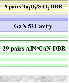
In our previous work, the characteristics of an optical pumped GaN-based VCSEL was successfully fabricated and investigated. The schematic diagram of the overall VCSEL structure are shown in the Fig. 4.1 . The hybrid DBR VCSELs structure is composed of 2-inch diameter c-plane sapphire , 2um thickness GaN buffer layer , 29 pairs AlN/GaN DBR , 5λ GaN cavity and 8 pairs Ta2O5/SiO2 upper DBR. The
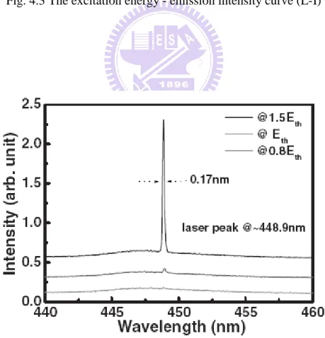
reflectivity of lower and upper DBR are all about 99%. A narrow PL emission with full width at half maximum of 0.21nm corresponds to the cavity resonant mode at 454.3nm was observed, as shown in Figure 4.2. The cavity quality factor, estimated from the emission linewidth of 0.21nm, was about 2200. Figure 4.3 shows the laser action was achieved under the optical pumping at room temperature with a threshold pumping energy (Eth) of about 55 nJ corresponding to an energy density of 7.8
mJ/cm2. A dominant laser emission line at 448.9 nm appearing above the threshold pumping energy is shown in the Fig.4.4.
25
Fig. 4.1 The schematic diagram of the optical pumped VCSEL structure
26
Fig. 4.3 The excitation energy - emission intensity curve (L-I)
27
4.1.2 CW lasing of current injected GaN-based VCSEL at 77k
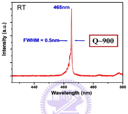
With the achievement of optically pumped GaN-based VCSEL, the realization of electrically-injected GaN-based VCSEL has become promising. Fig. 4.5 is the overall
current injected VCSEL structure. The resonant cavity structure has an 0ne optical
wavelength thickness ITO layer deposited on the p-type GaN layer compared with
optical pumped cavity. The ITO layer can be used as a transparent conduct layer(TCL)
and improve the current spreading problem resulting from low conductivity of p-GaN.
In addition ,One optical wavelength thickness can match the resonance phase
condition of microcavity and reach high transmittance(~98%) for ITO layer.
However , we can find that the quality factor of electrically pumped cavity is about
900 from PL spectrum , as shown in Fig. 4.6. The value of quality factor is about half
of the optical pumped result due to additional ITO absorption. We consider the loss of
ITO maybe one of the main challenges for us to reach CW lasing in current injected
VCSELs at room temperature.
In order to observe the lasing behavior in current injected VCSEL, we packaged
our devices into TO can. The packaged VCSEL device was mounted inside a
cryogenic chamber for testing under cw current injection condition using a cw current
source at 77 K. Fig. 4.7 shows the light output power versus cw injection current
28
output power showed a distinct threshold characteristic at the threshold current (Ith)
of about 1.4 mA and then was linearly increased with the injection current beyond the
threshold. The threshold current density is estimated to be about 1.8 kA/cm2 for a
current injection aperture of 10 um in diameter, assuming the current is uniformly
injected within the aperture. The lasing wavelength is 462.8nm with 0.15nm line
width shown in Fig. 4.8. The inset of Fig3.8 is the CCD image of the spatial l
emission pattern slightly below threshold. We believe the nonuniformity in the
emission intensity across the aperture could be due to the In nonuniformity that
creates a nonuniform spatial gain distribution in the emitting aperture as reported
29
Fig. 4.5 The schematic diagram of the current injected VCSEL structure
30
Fig. 4.7 The light output intensity vs injection current and current–voltage characteristics of GaN VCSEL
Fig. 4.8 The laser emission spectrum at different injection current levels measured at 77 K.
31
4.2 The design of electrical pumped VCSEL
4.2.1The reflectance and quality factor simulation with different ITO thickness
So far, our group have fabricated and demonstrated the CW operation of an electrically pumped GaN-based VCSEL at 77 K. Next step, we should work toward the cw lasing of current injected devices at room temperature. In order to reach the goal, we try to reduce the loss of ITO so that the threshold current can also be lower at room temperature. In general, the thinner layer has the smaller absorption for the same material, so we would like to replace previous one optical wavelength thickness ITO with thinner ITO layer.
Figure show the simulation cavity structure with different ITO layer thickness from 0 nm, 30 nm, 120 nm, 210 nm, and 225 nm. Here, the 225nm-thick ITO layer stands for one optical wavelength thickness at 440nm. Owing to DBR reflectivity symmetry, the we chosen 18-pair AlN/GaN DBR. Figure is the simulated reflectance spectra under different ITO thickness. The dip positions in the reflectance spectra represent the cavity modes with different ITO thickness and the quality factor can be estimated from the linewidth of the dip. In
Figure, the cavity mode wavelength is the function of different ITO thickness. The cavity mode wavelength shifts to longer wavelength because of the longer cavity length, but the cavity mode wavelength would turn back to shorter wavelength when ITO thickness is thicker than 120nm due to the exceeding of the stop band region of the lower DBR. In this case, the cavity mode would jump to the (m+1)th mode from the mth mode. Furthermore, the cavity mode also changes to multimode owing to longer cavity length and smaller mode spacing when ITO thickness is larger than 30nm. In Figure , the quality factor is about 700 using the cavity with a 225nm-thick
32
ITO layer, but this value is much lower than that without ITO layer of about 3300. If we consider the qualify factor of the cavity with a 30nm-thick ITO layer, the value of about 3100 is a little smaller than that with a 0nm-thick ITO layer but the structure with a ITO layer can be efficiently injected current in our electrical pumped VCSEL devices. Base on the simulation results and reality device requests, we can expect the 30nm ITO layer can efficiently reduce the loss and threshold current density of our VCSEL devices.
Figure 4.9 The simulation cavity structure
33
Figure4.11the simulated cavity mode with different thickness of ITO
34
4.2.2Design structure of electrical pumped device
For a typical VCSEL, the cavity length is designed to be 1 lambda or 3/2 lambda, so the antinode of optical field and active region could be easily designed to match each other. However, in our design, the cavity length has been determined to be seven-λ (optical length), which correspond to a geometric thickness of about 1.1 μm, due to the consideration of device fabrication. The structure should compose of a top dielectric reflector, a ITO layer, a p-type GaN, MQWs, an n-type GaN, and a bottom nitride-based reflector. The optimal thickness of the ITO layer to be about 30 nm, the p-type InGaN to be about 2 nm, the p-type GaN to be about 110 nm, of the p-type AlGaN as a electron blocking layer to be about 24 nm, of 10-pair In0.2Ga0.8N(2.5
nm)/GaN(12.5nm) multi-quantum wells (MQWs) to be about 150 nm, and of the n-type GaN to be about 860 nm, and slightly modified these thicknesses to make the center of MQWs and the ITO layer at the anti-node and node of optical field, respectively. Figure shows the electric field intensity (EFI) and the refractive index as the functions of the distance from top layer. From the figure, it can be observed that a pronounced resonant enhancement of the electric field was built up in the active region. It suggests that the light could be amplified inside the resonant cavity and the more opportunity could be obtained to achieve laser operation.
35
Figure 4.13 Electric field intensity (red line) and refractive index (black line) as a function of the distance from top layer.
4.3 Fabrication process of GaN-based VCSELs
To fabricate the VCSELs device on chip , we need to experience six process steps. Fig 4.14 is the schematic diagram of overall VCSELs process flowchart. In the beginning , SiNx mesa etching mask and ICP dry etching machine were used to define the mesa region . As shown in Fig 4.15, we check the electrically properties by probe station after mesa was finished. Then, 200nm SiNx layer was deposited by PECVD and patterned to form current confinement layer with effective current aperture varying from 15um to 40um. The four different structure ITO , which was mentioned earlier , were deposited individually by E-gun or sputter , and annealed at RTA system under nitrogen ambient. The ITO transparent conduct layer on a 40um current aperture after etching is shown in Fig 4.16. The Ti/Al/Ni/Au and Ni/Au contacts was deposited to serve as n-type and p-type electrode, respectively. The final step is deposition of 10pairs SiO2/Ta2O5 dielectric DBR as upper mirror. The
schematic diagram of completed electrical pumped VCSEL is shown in Fig 4.17 , and Fig4.18 is the OM image of VCSEL device with 5um metal aperture when current
36 injects.
Fig 4.14 The schematic diagram of overall VCSELs process flowchart
37
Fig 4.16 The ITO transparent conduct layer deposited on current aperture
38
Fig 4.18 The OM image of completed VCSEL device when current injects
4-4 Characteristics of optically pumped GaN-based VCSELs
The overall optical pumped GaN VCSEL structure is shown in Fig 4.19 The mirocavity and bottom DBR structure are grown in a vertical-type MOCVD system (EMCORE D75), which can hold one 2-inch sapphire wafer. The nitride-based DBR used in the experiment is the stacks of 29-pair AlN/GaN layers with insertion of the AlN/GaN super-lattice (SL). The super-lattice in structure is inserted for releasing strain during the growth of AlN/GaN DBR to further improve interface and raise reflectivity of the DBR. Fig4.20 is the reflectance spectrum of bottom DBR, and there is a high reflectivity (~99.3%) at 440nm. The stop band of bottom DBR is as wide as about 20nm.
Then, a micro-cavity formed by a p-n junction was grown following the growth of the DBR structure. The micro-cavity composed of about 860-nm-thick n-type GaN, a
39
ten pairs In0.2Ga0.8N/GaN (2.5 nm/7.5 nm) MQW, 24nm AlGaN electron blocking
layer, a 115-nm-thick p-type GaN and 2nm InGaN layer. The cavity length is about 7-λ in optical length. The 2nm InGaN layer is used for reduction the Schottky barrier height between ITO and p type GaN layer[37], and it can also improve current spreading when current inject. The SEM cross-section image is shown in Fig4.21 , and Fig4.22 are the PL spectrum and reflectance spectrum of VCSEL sample without upper DBR. Obviously, the cavity mode is at about 435nm.
The final process to complete a VCSEL is the deposition of a dielectric mirror. The dielectric mirror in the experiment, an eight pairs Ta2O5/SiO2 DBR, was deposited
using the electron beam evaporation. The dielectric mirror was coated onto as-grown sample surface in an O2 ambient at the controlled temperature about 150℃. The reflectivity spectrum of the dielectric mirror was measured as shown in Fig 4.23 The Ta2O5/SiO2 DBR shows a very high reflectivity as high as 99% centered at 450 nm
with a wide stop-band of about 100 nm.
Fig4.24 is the PL spectrum of GaN-based VCSEL with bottom and upper DBR. The cavity mode wavelength is about 440nm with a 0.24nm linewidth , and the quality factor estimated from PL spectrum is as high as 1900. The lasing behavior can be observed under optical pumping at room temperature in Fig4.25 . The threshold pumping energy density is about 3.3mJ/cm2, and this lower value compared with the previous result of our group represents the improvement of epitaxial quality, so that the internal loss and threshold energy density is reduced. Fig4.26 shows the lasing spectrum above the threshold condition, and the lasing wavelength is 438nm with a 0.15nm linewidth.
40
Fig 4.19 The schematic diagram of the optical pumped VCSEL structure
Fig 4.20The reflectance spectrum of bottom DBR 380 400 420 440 460 480 500 0 20 40 60 80 100 R e fl e c ta n c e (% ) Wavelength(nm) R ~99.3%
41
Fig 4.21 The cross section SEM image of VCSEL cavity without upper DBR
Fig 4.22 the PL and reflectance spectrum of VCSEL without upper DBR
380 400 420 440 460 480 500 -0.5 0.0 0.5 1.0 1.5 2.0 2.5 3.0 3.5 4.0 r e fl e c ta n c e (% ) wavelength(nm) in te n si ty (a .u ) 0 20 40 60 80 100
42
Fig 4.23 The reflectance spectrum of upper DBR
Fig 4.24 The PL spectrum of optical pumped VCSEL with upper DBR 350 400 450 500 550 600 0 10 20 30 40 50 60 70 80 90 100
R
e
fl
e
c
ta
n
c
e
(%
)
wavelength(nm)
R~99% 430 435 440 445 450 0 1 2 3 4 In te n s it y (a rb . u n it )Wavelength(nm)
439.9nm 0.23nm43
Fig 4.25 The pumping energy density versus normalized intensity diagram
Fig 4.26 The lasing spectrum of optical pumping VCSEL
0.0 0.5 1.0 1.5 2.0 2.5 3.0 3.5 4.0 4.5 5.0 5.5 0 2 4 6 8
N
o
rm
a
li
ze
d
i
n
te
n
s
it
y
(a
.u
)
Pumping energy density (mJ/cm
2)
Threshold energy density~3.3mJ/cm2
430 435 440 445 450 1 2 3 4 5 6 7
In
te
n
s
it
y
(a
rb
.
u
n
it
)
Wavelength(nm)
438.4nm FWHM~0.15nm44
4-5 Characteristics of electrically pumped GaN-based VCSELs
We report the demonstration of the CW laser action on GaN-based vertical cavity surface emitting lasers (VCSEL) at room temperature. The laser structure consists of a 10-pair Ta2O5/SiO2 distributed Bragg reflector (DBfR), a 7λ-thick optical cavity, 10
pairs InGaN/GaN multi-quantum wells with an AlGaN electron blocking layer, and a 29-pair AlN/GaN DBR. The laser has a threshold current of about 9.7 mA corresponding to the current density of about 12.4 kA/cm2 and a turn-on voltage about 4.3 V at 300K. The lasing wavelength was 412 nm with a linewidth of about 0.5 nm. A spontaneous emission coupling efficiency factor of about 5×10⁻³ and the degree of polarization of about 55% were measured, respectively. The laser beam has a narrow divergence angle of about 8o.
GaN-based materials have attracted a great attention since the early 1990s due to the wide direct band gap and the promising potential for the optoelectronic devices such as light emitting diodes (LEDs) and laser diodes (LDs) [38-39]. So far, GaN-based edge emitting lasers have been demonstrated and applied in commercial products for high density optical storage applications. However, the vertical cavity surface emitting lasers (VCSELs), with superior characteristics such as the single longitudinal mode emission, low divergence angle, and array capability, are still under development and currently gaining much attention. Optically pumped GaN-based VCSELs have been reported by using different kinds of optical cavity structures, such as dielectric distributed Bragg reflectors (DBR) VCSELs with cavities consisting of dielectric top and bottom DBRs [40], and hybrid DBR VCSELs with cavities consisting of epitaxially grown nitride bottom DBRs and dielectric top DBRs [41]. We have recently demonstrated the CW current injection of GaN-based VCSEL with
45
hybrid mirrors at 77K in 2008 [42]. Subsequently, the room temperature operation of GaN-based VCSEL devices was reported using optical cavities sandwiched by double dielectric DBRs [43,44]. The major improvements of their devices to achieve room temperature operation are by using a thinner transparent conducting layer of about 50 nm to reduce the internal optical loss and by using the GaN substrate to ensure the good crystal quality of active layers. However, to form VCSELs with double dielectric DBRs required complex fabrication process, such as laser lift-off or elaborated polishing and bonding process [45]. In this paper, we report the achievement of CW room temperature lasing with hybrid DBR cavity and a thin Indium-Tin-Oxide (ITO) layer of 30 nm as the transparent conducting layer combining with a thin heavily doped p-type InGaN contact layer to reduce the optical loss while maintaining good current spreading capability. Moreover, we inserted an AlGaN electric blocking layer on the top of the InGaN multiple quantum well (MQW) to prevent the carrier overflow [46]. The lasing characteristics such as laser output power and device voltage versus injected current characteristics, degree of polarization, divergence angle, and spontaneous emission coupling factor have been measured and investigated.
Fig. 4-27(a) shows the schematic diagram of the whole GaN-based VCSEL structure. In the structure, the positions of the ITO layer and MQWs region are located at the node and anti-node positions of the electric field, respectively to reduce the absorption from the ITO layer and to further increase the coupling between the electric field and MQWs region. The VCSEL structure was grown on a 2-inch sapphire substrate by the metal-organic chemical vapor deposition (MOCVD) system. The substrate was thermally cleaned in the hydrogen ambient for 5 min at 1100 °C, and then a 30 nm-thick GaN nucleation layer was grown at 500°C. The growth temperature was raised up to 1100 °C for the growth of a 2 µm-thick GaN buffer layer.
46
The subsequent epitaxial structure consisted of a 29-pair AlN/GaN DBR, a 7 cavity ( = 410 nm) including a 860 nm-thick n-GaN layer, 10 pairs InGaN/GaN (2.5 nm/12.5 nm) MQWs, a 24 nm-thick AlGaN layer as the electron blocking layer, a 110 nm-thick p-GaN layer, and a 2 nm-thick p+ InGaN layer as the contact layer. The AlGaN electron blocking layer was served to reduce the electron overflow to the p-GaN layer. In order to reduce the crack problems encountered in the AlN/GaN DBRs, we inserted one AlN/GaN superlattice into each five DBR periods at first twenty pairs of DBR. Then the superlattice was inserted into each three DBR periods for the remaining nine pairs of DBR to reduce the tensile strain [47]. In the fabrication process, a 200 nm-thick SiNx layer was deposited by the plasma enhanced chemical vapor deposition as a current confined layer. By this way, the current injection aperture of VCSEL devices was about 10 m in diameter. Then, a 30 nm-thick ITO layer was deposited as the current spreading layer due to the poor conductivity of the p-GaN layer and annealed at 600 oC for 10 min by rapid thermal annealing. The 2 nm-thick p+ InGaN layer on the p-GaN surface can further reduce the series resistance between the thin ITO layer and the p-GaN layer with a slight increase of absorption. Then, the p-contact and n-contact were deposited with Ni/Au of about 20 nm/150 nm and Ti/Al/Ni/Au of about 20 nm/150 nm/20 nm/150 nm by the e-gun system, respectively. Finally, 10 pairs Ta2O5/SiO2 of the top dielectric DBR were deposited by
the ion-assisted e-gun system to complete the whole GaN-based VCSEL devices. Both of the 29-pair AlN/GaN DBR and the 10-pair Ta2O5 DBR show a high
reflectivity of over 99 % at the peak wavelength at 410nm in the n-k measurement system. Fig. 4-15(b) shows the charge-coupled device (CCD) image of a VCSEL device injected at 2 mA under CW current injection at room temperature
47
. Fig. 4-27(a)VCSEL full structure (b)turn on image at 2mA
The GaN-based VCSEL devices with current injection apertures of about 10 μm in diameter were tested by using a Keithely 238 CW current source. The emission light was collected by a 100 m diameter multimode fiber and fed into the spectrometer using a grating of 1800 g/mm with a spectral resolution of about 0.15 nm. The output from the spectrometer was detected by a CCD to record the emission
48
spectrum. The VCSEL devices were then measured at environment temperature at 300 K. Fig. 4-28(a) shows L-I-V curves at 300 K. The dash line is the linear fitting curve of the laser intensity versus injection current. A clear lasing transition from spontaneous emission to stimulated emission can be observed at room temperature. From the linear fitting curve, the laser threshold current is around 9.7 mA corresponding to the current density of about 12.4 kA/cm2. The relative low threshold at room temperature operation could be due in part to the successful prevention of carrier overflow by using the electron blocking layer on top of the MQWs and the lower internal absorption loss of the thinner ITO layer. The turn-on voltage is about 4.3 V indicating the good electrical contact of the 30 nm ITO transparent layer and the 2 nm-thick InGaN layers. The output laser intensity from the sample increased linearly with current injection beyond the threshold current. However, the laser intensity started to roll over at higher injection current beyond 15 mA due to the thermal effect. We estimated the spontaneous emisson coupling factor from the log-log plot of L-I curve as shown in Fig. 4-28(b). The data points are matched well to the solid fitting line calculated from microcavity laser rate equations [48]. From the curve, we obtained an estmated β value of about 510-3.
49
Fig. 4-28(a)LIV curve at 300k (b) coupling factor from the log-log plot of L-I curve
50
Fig. 4-29(a) shows the emission spectra of our GaN-based VCSEL devices at current injection of 0.6 Ith, 1 Ith and 1.2 Ith, respectively. The laser emission
wavelength was measured to be 412 nm with a linewidth of about 0.5 nm. The inset of Fig. 4-29(b) shows the CCD image of a lasing spot size of about 2 m in diameter. Finally, using the angular-resolved measurement system, the laser intensity at different angles emitted from the GaN-based VCSELs was collected by using a 600 m fiber. Fig. 4-29(b) shows the measurement data at different angles and the solid curve is the fitting curve. We obtained a laser beam divergence angle of about 8o. Fig. 4-29(c) shows the degree of polarization (DOP) of the laser beam. The solid line is the fitting curve. The DOP value was estimated to be about 55o.