行政院國家科學委員會專題研究計畫 期中進度報告
微/奈米技術於 N x N 光開關系統之發展--子計畫二:NxN
複合式光開關之研製(2/3)
期中進度報告(精簡版)
計 畫 類 別 : 整合型
計 畫 編 號 : NSC 95-2221-E-002-239-
執 行 期 間 : 95 年 08 月 01 日至 96 年 07 月 31 日
執 行 單 位 : 國立臺灣大學機械工程學系暨研究所
計 畫 主 持 人 : 楊燿州
報 告 附 件 : 出席國際會議研究心得報告及發表論文
處 理 方 式 : 期中報告不提供公開查詢
中 華 民 國 96 年 05 月 31 日
行政院國家科學委員會補助專題研究計畫
□ 成 果 報 告
■期中進度報告
微/奈米技術於NxN光開關系統之發展
-子計畫二:NxN複合式光開關之研製(2/3)
計畫類別:□ 個別型計畫 ■ 整合型計畫
計畫編號:NSC 95-2221-E-002-239-
執行期間:
95 年 8 月 1 日至 96 年 7 月 31 日
計畫主持人:楊燿州
共同主持人:范光照,鍾添東
計畫參與人員: 廖柏亭,郭崎煒
成果報告類型(依經費核定清單規定繳交):■精簡報告 □完整報告
本成果報告包括以下應繳交之附件:
□赴國外出差或研習心得報告一份
□赴大陸地區出差或研習心得報告一份
■出席國際學術會議心得報告及發表之論文各一份
□國際合作研究計畫國外研究報告書一份
處理方式:除產學合作研究計畫、提升產業技術及人才培育研究計畫、列
管計畫及下列情形者外,得立即公開查詢
□涉及專利或其他智慧財產權,□一年□二年後可公開查詢
執行單位:國立台灣大學機械工程研究所
中 華 民 國
96 年 5 月 30 日
微/奈米技術於
NxN 光開關系統之發展
-子計畫二:NxN 複合式光開關之研製(2/3)
計劃編號:NSC 95-2221-E-002-239-
執行期限:95/8/1 - 96/7/31
計畫主持人:楊燿州副教授
國立臺灣大學 機械工程研究所
中文摘要
本計劃旨在發展以微機電技術為基礎
的
NxN 光開關系統。為滿足光開關微小化
之目的,本計劃設計一種具備有大位移量、
及雙穩態(bi-stable)閂鎖功能之新型微致動
元件,以應用於
NxN 光開關系統之發展。
該微致動元件由雙穩態機構、電熱式
V 型樑
致動器(electrothermal V-beam actuator)、及微
鏡面所組成。此外,該微致動元件可利用
SOI(Silicon-On-Insulator)晶圓,搭配深反應
離子蝕刻製程
(deep reactive ion etching,
DRIE),及氫氧化鉀(KOH)蝕刻液將晶圓背
面部分掏空,以懸浮微鏡面之製程等,完成
元件之製作。由初步的實驗量測結果顯示,
當輸入
20 伏特直流電壓時,可移動微鏡面
約
125µm 之距離。
關鍵字:光開關、微致動器、雙穩態結構、
微機電技術
Abstract
In this work, we develop a MEMS-based
NxN optical switch. For the miniature of the
optical switch, a novel design of micro-
actuator is presented. The micro-actuator
consists of the bi-stable mechanism,
electrothermal V-beam actuators, and the
micro-mirror. This micro-actuator is able to
produce large displacement and have latching
function. The micro-actuator device is realized
by using deep reactive ion etching (DRIE) on a
SOI (Silicon-On-Insulator) wafer. The
backside of the SOI wafer is partially etched to
ensure that the micro mirror can be completely
released. The preliminary measurement is also
performed. The displacement of the micro
mirror can achieve at least 125µm under a
driving voltage of 20V.
ㄧ
.前言
在現代的光纖通訊網路系統中,光開關
扮演著切換光訊號的重要角色,亦即光開關
擁有將訊號由輸入端切換至特定輸出端之
功 能 , 進 而 可 達 成 光 塞 取 多 工
(optical
add-drop multiplexer,OADM)、光交換連結
(optical cross connect,OXC)、及網路保護
(network protection)等功能。以目前趨勢觀
之,光開關皆朝向全光式切換(all optical
switching)發展,以增加訊號傳輸的頻寬與速
度,以往透過光電轉換的傳輸方式,則逐漸
被全光式切換所取代。
目前已有許多不同的技術,用於全光式
切 換 之 光 開 關 的 發 展 , 例 如 熱 光 技 術
(thermo-optics)[1]、液晶(liquid-crystal)技術
[2]、及微機電技術(microelectromechanical
systems,MEMS)[3-4]等。在這些技術當中,
微機電技術則取得領先的地位,因為微機電
技術運用了半導體製程,使得所製造出的元
件不僅擁有高精準度、同時又有微小化的優
點,而且更具有批次量產的能力,因此可降
低生產成本。是故,微機電技術在光通訊元
件的發展上,必然有其舉足輕重的地位。
二
.文獻探討
近幾年來,已有眾多國內外的研究團
隊,發表了以微機電技術為基礎的NxN光開
關[5-10]。在這些微機電式光開關中,若依
驅動方式區別,又可區分為靜電式驅動[5-7]
或電磁式驅動[8-10]。以下則將針對具有代
表性的參考文獻,做進一步的探討。
Kuo 等 人 [5] 利 用 MUMPs (multi-user
MEMS processes)製程,設計製造一具有彎曲
型翹翹板結構之微致動器,微鏡面則設置於
彎曲型翹翹板的兩端,並以靜電力將彎曲型
翹翹板吸引向下,藉此控制微鏡面之位置,
達成切換光路的目的。Mi等人[6]與Chu等人
[7],則是使用體型微加工(bulk micromaching)
製造鏡面陣列,並透過靜電力吸引鏡面,進
而使得鏡面旋轉,以控制光訊號的行進路
線,達到開關目的。Hsieh等人[8]利用SOI
晶圓,以濕蝕刻法(wet etching)在晶圓背面,
蝕刻出垂直鏡面,並以深反應離子蝕刻、金
屬鍍膜等製程,於晶圓正面,定義元件之幾
何結構、導電線圈等。因此,當電流通過線
圈時,產生電磁力進而帶動鏡面的運動,達
成切換之目的。Huang等人[9],結合面型微
加工(surface micromaching)及磁性材料之電
鍍,定義出定義元件結構、鏡面及導電線
圈,因此當電流通過線圈時,產生電磁力進
而 帶 動 鏡 面 的 運 動 , 達 成 開 關 之 目 的 。
Horsley等人[10],則利用SOI晶圓及深反應
離子蝕刻,定義元件結構及鏡面,接著再鍍
上磁性材料,並透過外加磁場,控制鏡面之
旋轉,達成切換光路的目的。
可動式鏡面 輸入 端光 纖 輸出端光纖(a)
可動式鏡面 輸入端光纖 輸出端光纖(b)
圖1 (a)傳統的 NxN 光開關之光路設計,存在光路徑 不等長的缺點。 (b)改良型 NxN 光開關之光路設計, 其光路徑均等長。三
.研究方法
傳統的
NxN 光開關,其光路設計,如
圖
1(a)所示,此種光路架構,存在光路徑不
等長的缺點,因此,要使得每種光路徑的光
學特性相同,並不容易。有鑒於此,Chu 等
人[11]提出一種改良型的 NxN 光路設計,使
得每種光路徑等長,如圖
1(b)所示,在這種
光路架構之下,由於光路徑均等長,所以,
其光學特性較容易一致。因此,本計劃將採
用此改良型的
NxN 光開關之光路設計。
不管是傳統的
NxN 光開關,或是改良
型的
NxN 光開關,都需要「可動式鏡面」,
以反射光訊號至特定的輸出端。因此,本計
畫設計製造一種新型微致動元件,以控制
「可動式鏡面」,使其可以達成切換光訊號
之目的。此一新型微致動元件必須具備有大
位移量,亦即至少可產生
250µm 之位移,以
完全覆蓋反射光束,同時也需具備雙穩態之
功能,使得鏡面能夠停留在兩個穩定的位
置,而不需要消耗額外的能量。
雙穩態結構在微機電領域中,已有廣泛
的應用。雙穩態結構可由兩條平行的曲型樑
(curved beam)所組成,並於中心部分將兩條
曲型樑夾持固定,以避免曲型樑產生旋轉翹
曲的運動。曲型樑的形狀乃為直型樑受軸向
負荷(axial loading)時,所產生的第一挫曲模
態(first buckling mode)[12],如圖 2 所示。由
於雙穩態結構提供兩個穩定的狀態,分別如
圖
2(a)、(b)所示。所以,雙穩態結構具有閂
鎖(latching)之功能。然而,由於大位移量
(250µm)的需求,所以,雙穩態結構的中心
第一穩態 (初始位置) 第二穩態 δ y x l w (a) (b) 圖2 雙穩態結構 (a)第一穩態(初始位置) 。(b) 第二 穩態。 表1 雙穩態結構的設計尺寸 曲型樑寬度(w
) 8µ
m
曲型樑長度(l
) 4000µ
m
曲型樑中心初始偏移量(δ ) 125µ
m
-150 -100 -50 0 50 100 150 -2500 -1500 -500 500 1500 2500 3500 外加施力 (µN) 雙穩 態結 構之 頂端 位置 (µm ) forward-moving backward-moving 圖3 外加施力於雙穩態結構之中心頂端位置時,外 加施力與中心頂端位置之模擬結果圖。(此模擬結果 之座標系統如圖2(a)所示)初始偏移量(δ)即設計為 125µm,其詳細尺寸
如表
1 所列。本計畫採用微機電模擬軟體
CoventorWare 2006,進行雙穩態結構的力學
分析,當於雙穩態結構的中心頂端外加施力
時,待外加施力超過一臨界值時,可使得雙
穩 態 結 構 由 第 一 穩 態 的 初 始 位 置 , 跳 躍
(snap-through)至第二穩態。由圖 3 的模擬結
果可知,外加施力必須大於
2000µN,方可
讓雙穩態結構由第一穩態,跳躍至第二穩
態。然而,這也表示了負責推動雙穩態結構
的致動器,所輸出的力量必須大於
2000µN,
而且該致動器也必須可以產生超過
125µm
以上的位移量,方能成功推動雙穩態結構。
如此一來,為產生如此大的位移量,將會使
得致動器的尺寸過大。因此,本計畫將結合
雙 穩 態 結 構 , 與 電 熱 式
V 型 樑 致 動 器
[13](electrothermal V-beam actuator),設計出
一種新型的微致動元件。
微鏡面 V 型樑致動器 雙穩態結構 彎鉤 L 型鉤 圖4 新型微致動元件之示意圖。
本計畫所提出之新型微致動元件,如圖
4 所示。此元件包括雙穩態結構、微鏡面、
二組設置於雙穩態結構側邊的
V 型樑致動
器(以下稱「側向 V 型樑致動器」)、負責拉
引雙穩態結構向下的另一組
V 型樑致動器
(以下稱「縱向 V 型樑致動器」)、設置於雙
穩態結構之
L 型鉤、及設置於縱向 V 型樑致
動器之彎鉤。此新型微致動元件的操作流
程,則如圖
5 所示。首先,驅動側向 V 型樑
致動器,將雙穩態結構由曲型樑拉成直型
樑 , 降 低 雙 穩 態 結 構 的 跳 躍 能 障
(energy
barrier),同時使得 L 型鉤與彎鉤相互對準。
接著,再驅動縱向
V 型樑致動器,使得彎鉤
能夠帶動
L 型鉤向下運動,進而讓雙穩態結
構得以越過中心線,如圖
5(b)所示。最後,
先移除側向
V 型樑致動器的驅動電壓,再移
除縱向
V 型樑致動器的驅動電壓,使得雙穩
態結構能夠停止於第二穩態。
驅動側向
V 型樑致動器,將雙穩態結構
由曲型樑拉成直型樑,除了可以降低雙穩態
結構的跳躍能障外,更有「側向小位移、鏡
面大位移」的優點。由圖
6 的模擬結果可知,
雖然所需的側向施力較大,但是側向位移量
小於
5µm,卻有超過 100µm 的縱向位移量,
L θ W(a)
(b)
(c)
圖5 新型微致動元件之操作流程圖 (a)驅動側向 V 型樑致動器 (b)驅動縱向 V 型樑致動器 (c)移除所有 的驅動電壓,雙穩態結構停止於第二穩態。0 20 40 60 80 100 120 0 5000 10000 15000 20000 側向施力 (µN) 微鏡面位移 (μm ) 0 1 2 3 4 5 6 7 8 側向位移 (μ m ) 圖6 外加施力於雙穩態結構之側邊時,外加的側向 施力與微鏡面位移、側向位移之模擬關係圖。
亦即能夠移動微鏡面超過
100µm 的距離。另
一方面,由模擬結果亦確認得知,所設計的
L 型鉤與彎鉤的相對位置,在驅動側向 V 型
樑致動器時,L 型鉤可以順利移至彎鉤之
下,並相互對準,而不會互相碰撞。新型微
致動元件的雙穩態結構,其詳細尺寸如表
1
所列,而側向與縱向
V 型樑致動器之詳細尺
寸,則如表
2 所列。
四
.製程流程
本計畫採用
SOI 晶圓,並使用兩道光
罩,以製作「新型微致動元件」,詳細的製
程流程,如圖
7 所示。起始材料為 SOI 晶圓,
其元件層(device layer)、犧牲層(buried oxide
layer)及基板層(handle layer)的厚度分別為
80
µ
m
、2
µ
m
及
500
µ
m
。首先,利用爐管法
(thermal oxidation)於 SOI 晶圓表面成長二氧
化矽層,再利用低壓化學氣相沉積(LPCVD)
氮 化 矽 層 。 接 著 , 利 用 微 影 製 程
(photo-
lithography)搭配第一道光罩,及反應式離子
蝕刻(Reactive Ion Etching,RIE),於 SOI 晶
圓背面定義
KOH 的蝕刻開孔。之後,使用
KOH 將 SOI 晶圓背面蝕刻穿透至犧牲層,
如圖
7(c)所示。同樣地,再利用微影製程搭
配第二道光罩,及反應式離子蝕刻,於
SOI
晶圓正面定義元件圖案,並由電感藕合電漿
(e) (d) (a) (b) (c) Au Si3N4 SiO2 Si (f) (g) Device layer Handle layer (h) shadow mask 圖7 製程流程 (a)於 SOI 晶圓成長二氧化矽及沉積 氮化矽 (b)SOI 晶圓背面之微影製程、反應式離子蝕 刻圖案轉移 (c)KOH 濕蝕刻 (d) SOI 晶圓正面之微影 製程、反應式離子蝕刻圖案轉移 (e)深反應離子蝕刻 (f)HF 蝕刻懸浮 (g)利用擋罩將 V 型樑致動器遮蔽 (h) 微鏡面濺鍍上金。 表2 V 型樑致動器的設計尺寸 V型樑致動器 側向 縱向 V型樑長度(L) 2800µ
m
3000µ
m
V型樑寬度(W) 22µ
m
10µ
m
V型樑與水平夾角(θ) 0.6度 0.6度 V型樑數量 45組 10組蝕刻機(Inductive Coupling Plasma Etcher,
ICP),進行深反應離子蝕刻製程,將元件結
構蝕刻製造出來。值得一提的是,由於深反
應離子蝕刻過程當中,必須有晶圓散熱的考
量,但是,SOI 晶圓背面已有部份被掏空,
所以掏空的部份,必然使得晶圓散熱能力大
幅降低,如此一來將會導致
SOI 晶圓正面的
元件結構,無法成功蝕刻出來。因此,本計
劃乃將
SOI 晶圓背面的掏空部份,填入散熱
膏(AI Technology, Inc.),增加晶圓背面的散
熱能力。待元件結構蝕刻製造出來後,再利
用氫氟酸(hydrofluoric acid,HF),將可動結
構底下的犧牲層完全蝕刻掉,使得可動結構
懸空。此外,雖然微鏡面的面積很大,但是
由於鏡面底下事先已經利用
KOH 掏空,所
以,氫氟酸仍然可以將微鏡面完全懸浮。最
後,為了提高光學反射率,利用濺鍍的方
式,將微鏡面鍍上金,金的濺鍍厚度大約為
1500Å。另外,為維持 V 型樑致動器整體的
電阻性,
V 型樑致動器上面皆以擋罩(shadow
mask)遮蔽,因此,V 型樑致動器並不會有
金濺鍍覆蓋。同時,由於濺鍍製程的均勻性
(conformity)並不好,所以,僅有元件的表面
及側壁部分,有金濺鍍其上,而結構層底下
的犧牲層部分,則沒有濺鍍到金,因此,結
構層與基板層的絕緣性仍可保持。
五
.實驗結果與討論
新型微致動元件之
SEM 圖,包含雙穩
態結構、微鏡面、V 型樑致動器、L 型鉤及
彎鉤等,如圖
8 所示。由圖 8(d)、(e)可觀察
出,大面積的微鏡面已經成功被懸浮起來,
而且沒有黏附(stiction)的現象發生。
為 確 定 新 型 微 致 動 元 件 之 雙 穩 態 結
構,是否存在兩個穩定位置,因此,先利用
探針以機械力推動雙穩態結構,將微鏡面由
初始位置推至第二穩態,實驗結果發現,微
鏡面、雙穩態結構均可以成功地停留在第二
個穩定位置,如圖
9(b) ~ 圖 9 (e)所示。換言
之,微鏡面於機械力推動之下,得以移動約
(a) (b) (c) 圖8 新型微致動元件之 SEM 圖 (a)新型微致動元件 整體結構 (b)新型微致動元件細部放大 (c)V 型樑致 動器。(d) (e) (f) 圖8 (續) 新型微致動元件之 SEM 圖 (d)微鏡面細部 放大 (e)由晶圓背面觀察之微鏡面細部放大 (f)L 型 鉤與彎鉤。 (a) (b) (c) 圖9 新型微致動元件之 CCD 圖 (a)微鏡面之初始位 置 (b)微鏡面移至第二穩態位置 (c)雙穩態結構移至 第二穩態位置。
(d) (e) (f) (g) 圖9 (續)新型微致動元件之 CCD 圖 (d)由晶圓背面觀 察之微鏡面初始位置 (e)由晶圓背面觀察微鏡面移至 第二穩態位置 (f) L 型鉤與彎鉤之初始位置 (g)驅動 側向V 型樑致動器後,L 型鉤與彎鉤之相對位置。
250µm 的大位移量。確認新型微致動元件存
在兩個穩定位置後,遂可施加電壓驅動元
件,由初步的實驗量測結果顯示,當輸入
20
伏特直流電壓,驅動側向
V 型樑致動器後,
微鏡面可移動約
125µm 之距離,同時,L 型
鉤可以順利移至彎鉤之下,並相互對準,而
不會互相碰撞,L 型鉤與彎鉤之初始位置及
驅動側向
V 型樑致動器後之相對位置,分別
如圖
9(f)、(g)所示,此一實驗量測結果,與
模擬結果十分穩合。
六
.結論
本計畫提出一種以微機電技術為基礎
的新型微致動元件,此新型微致動元件具備
大位移量、及雙穩態閂鎖之功能,以應用於
NxN 光開關系統之發展。此微致動元件可利
用
SOI 晶圓,搭配二道微影製程、深反應離
子蝕刻、KOH 濕蝕刻等製程,成功製造出
來。由初步的實驗量測結果顯示,
20 伏特直
流電壓驅動側向
V 型樑致動器後,可移動微
鏡面約
125µm 之距離,且 L 型鉤與彎鉤移
動後之相對位置,可以相互對準,與模擬結
果十分穩合。
七
.計畫結果自評與展望
本計劃目前已完成新型微致動元件之
初步的實驗量測,未來將繼續完成新型微致
動元件的後續量測工作,同時將使用此新型
微致動元件,以組裝
NxN 光開關,完成最
終的計畫目標。
References
[1] Y. O. Noh, J. M. Kim, M. S. Yang, H. J.
Choi, H. J. Lee, Y. H. Won, and S. G. Han,
“Thermooptic 2x2 asymmetric digital
optical switches with zero-voltage
operation state”, IEEE Photonics Tech-
nology Letters, vol. 16 , pp. 446-448, 2004.
[2] A. L. Zhang, K. T. Chan, M. S. Demokan,
W. C. Chan, C. H. Chan, H. S. Kwok, and
H. P. Chan, “Integrated liquid crystal
optical switch based on total internal
reflection”, Applied Physics Letters, vol.86,
pp. 211108, 2005.
[3] S. H. Jia, G. F. Ding, X. L. Zhao, C. S.
Yang, “Novel optic-fiber switches based on
the wobble-type MEMS electromagnetic
microactuator”,
Optics and Laser
Technology, vol. 39, pp. 353-358, 2007.
[4] R. Guerre, F. Fahrni and P. Renaud, “Fast
10-µs Microelectromechanical optical
switch inside a planar hollow waveguide
(PHW)”, Journal of Lightwave Technology,
vol. 24, pp. 1486-1498, 2006.
[5] J. N. Kuo, G. B. Lee, W. F. Pan,
“High-performance stress-induced micro-
machined optical switch with multi-
switching function using seesaw structure”,
Japanese Journal of Applied Physics, vol.
45, pp. 5030-5034, 2006.
[6] X. Y. Mi, H. Soneda, H. Okuda, O. Tsuboi,
N. Kouma, Y. Mizuno, S. Ueda, I. Sawaki,
“A multi-chip directly mounted 512-
MEMS-mirror array module with a
hermetically sealed package for large
optical cross-connects”, Journal of Optics
A: Pure and Applied Optics, vol. 8, pp.
S341-S346, 2006.
[7] P. B. Chu, I. Brener, C. Pu, S. S. Lee, J. I.
Dadap, S. Park, K. Bergman, N. H.
Bonadeo, T. Chau, M. Chou, R. A. Doran,
R. Gibson, R. Harel, J. J. Johnson, C. D.
Lee, D. R. Peale, B. Tang, D. T. K. Tong,
M. J. Tsai, Q. Wu, W. Zhong, E. L.
Goldstein, L. Y. Lin, and J. A. Walker,
“Design and nonlinear servo control of
MEMS mirrors and their performance in a
large port-count optical switch”, Journal of
Microelectromechanial Systems, vol. 14,
pp. 261-273, 2005.
[8] H. T. Hsieh, C. W. Chiu, T. Tsao, F. K.
Jiang, and G. D. Su, “Low-actuation-
voltage MEMS for 2-D optical switches”,
Journal of Lightwave Technology, vol. 24,
pp. 4372-4379, 2006.
[9] Z. L. Huang, and J. Shen, “Latching
micromagnetic optical switch”, Journal of
Microelectromechanical Systems, vol. 15,
pp. 16-23, 2006.
[10] D. A. Horsley, W. O. Davis, K. J. Hogan,
M. R. Hart, E. C. Ying, M. Chaparala, B.
Behin, M. J. Daneman, and M. H. Kiang,
“Optical and mechanical performance of a
novel magnetically actuated MEMS-based
optical switch”, Journal of Microelectro-
mechanical Systems, vol. 14, pp. 274-284,
2005.
[11]C. Chu, and J. Y. Zhou, “2-D optical
switch with lens mount”, United States
Patent, patent no. US 6937783 B2, 2005.
[12] J. Qiu, J. H. Lang and A. H. Slocum, “A
curved-beam bistable mechanism”,
Journal of Microelectromechanical
Systems, vol. 13, pp. 137-146, 2004.
[13] J. M. Maloney, D. S. Schreiber, and D. L.
DeVoe, “Large-force electrothermal linear
micromotors”, Journal of Micromechanics
and Microengineering, vol. 14, pp.
出席國際學術會議心得報告
計畫編號
NSC 95-2221-E-002-239-
計畫名稱
微/奈米技術於
NxN光開關系統之發展-
子計畫二:
NxN複合式光開關之研製(2/3)
出國人員姓名
服務機關及職稱
郭崎煒 台灣大學機械工程學系 碩士班研究生
會議時間地點 5/20~5/24, Santa Clara, Ca, US
會議名稱
NSTI Nanotech 2007
發表論文題目 Optimization of Disk-type Piezoelectric Transformers
一、參加會議經過
NSTI Nanotech 為一年舉辦一次的奈米科技會議。因為今年包含了 2007 TechConnect
Summit 以及 CleanTech 2007,所以本次會議內容涵蓋非常廣。主題除了奈米光電(Nano
Electronics & Photonics)、感測器系統(Sensors & Systems)、微機電系統(MEMS)、 奈米
機電系統(NEMS)、奈微米流體(Micro & Nano Fluidics)、奈米探管(Carbon Nano Structures
& Devices)、奈米材料與元件(Nanostructured Materials & Devices)等,還有更多關於健
康、環保、環境、能源、生化、醫療等議題。
在
2006 年 11 月,經由指導教授楊燿州博士鼓勵與指導下,投稿參加 2007 NSTI
Nanotech,至 2007 年元月,喜獲通知錄取論文並需於會中作 Poster Presentation。這次
的會議在加州的 Santa Clara Convention Center 舉行(圖 1)(圖 2)。正式議程排定日期為五
圖
2. 會議廳入口處
1. 五月 20 日
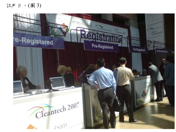
註冊日。(圖 3)
圖
3. 註冊地點
2. 五月 21 日
因為會議主題有包含
CleanTech 2007,所以會議開場是請 Shell Oil 的 J. Hofmeister
燃料電池以及生物燃料。還有利用奈米科技來保存傳統能源如石油、瓦斯等。最後他提
到了只有是人就有利用能源,於是乎人人都有責任去保護地球上的資源。之後,整個會
議分成了許多主題,有可撓性奈米技術、奈米探管、生物感測器、奈米製造等議題,在
各個會議室報告。
3. 五月 22 日
延續第一天的主題,依然在各個會議室舉行報告。而從這一天開始,展覽大廳開始
有廠商擺攤。他們介紹各個公司的技術以及提供資料給需要的人。筆者所屬的論
文”Optimization of Disk-type Piezoelectric Transformers”乃屬於微機電領域。此領域的
poster session 安排於此日的下午四點至六點。其中與許多外國人士交流意見以及有著愉
快的交談。(圖 4)(圖 5)
4. 五月 23 日
此日是
Cleantech 2007 實際開始的日期。開場由 V. Khosla 介紹 clean energy 的應用
以及未來的發展性。第二場是由
H.講如何有效的將 clean energy 轉換成電能還有次技術
所需要的條件及解決方案。從此日開始,各個會議室的議題也轉變成生物醫學應用相
關,如生物奈米(BioNano)等。
5. 五月 24 日
會議的最後一天,延續第三天的議題,還提到了生化材料(Bio Materials)以及奈米技
術的教育相關。而最後兩天也延續著
Cleantech 的主題,討論到了風、燃料以及再生能
源。
二、與會心得
此次很高興能在眾多的投稿者中(1745 人)錄取到 NSTI Nanotech 2007 的 Poster
session。也由於此會議的規模非常盛大,因此所涵蓋的領域亦十分廣泛。讓筆者除了在
自己的研究領域有更進一步的瞭解外,也提供了一個機會去見識其他領域的最新研究發
展。
與會期間能與世界各國的專業人士針對相關領域的議題討論與心得交換,對於自己
受益良多。對於此行的最大收穫就是利用張貼海報的同時能與不同領域的人才相互討
論,不僅訓練自己的英文溝通能力,也藉此認識朋友。對於未來研究與發展有著顯著的
助益。
此次的會議與廠商有著合作的關係,也讓筆者可以近距離的跟廠商接觸以及討論研
究相關與未來科技發展的議題。而且這次會議也有美國相關產業的龍頭來發表演講,讓
我瞭解了以世界科技大國所規劃未來產業的趨勢,以及對於世界日漸缺乏的能源他們的
因應之道。
此次參展也有許多台灣的與會者,因此也可看出台灣在奈米科技中扮演著相當重要
的角色。而透過這次的會議也讓許多台灣的科技研究成果展現出來。也透過會議與其他
國家的交流,對台灣的科技發展有莫大的幫助。
圖
4. 筆者攝於展覽廳入口處
Optimization of Disk-type Piezoelectric Transformers
Chi-Wei Kuo, Chia-Yu Kang, Ying-Yin Huang,
*Chih-Kung Lee, and Yao-Joe Yang
Department of Mechanical Engineering, National Taiwan University
*
Institute of Applied Mechanics, National Taiwan University
ADDRESS: No. 1, Roosevelt Rd., Sec. 4, Taipei, Taiwan EMAIL: [email protected]
ABSTRACT
In this work, we present the optimization works of two disk-type piezoelectric transformers (PTs), the single-output PT and the dual-output PT, by using the elite Genetic Algorithm (GA) and a finite-element solver. The design goal is to maximize the efficiency under the constraint that the voltage gain is greater than 50 for igniting CCFL. The design parameters are the dimensions of the output-electrode sections, the electrode areas, and the devices structure. With different electrical loading impedances, the voltage gain and the efficiency were computed using the finite element solver, NTUPZE. The results were also verified with measured data. The optimization process is parallelized by the MPI library and a PC cluster for improving the computation efficiency. The characteristics of the optimal designs with different loads are also calculated.
Keywords: Genetic algorithm (GA), piezoelectric
transformer, finite element method (FEM), multi-object optimization, parallel computations.
1 INTRODUCTION
Recently, liquid crystal displays (LCD) have become one of the standard digital output devices for personal/portable computers as well as consumer electronics. Also, LCD technology is proved to be one of the most promising technologies for the flat-panel TV. Each LCD panel requires a few cold cathode fluorescent lamps (CCFL) as backlight sources. A CCFL requires a high voltage source for ignition. Piezoelectric transformers (PT), which were proposed in 1954 by Rosen [1], step up or step down input voltages by electrical/mechanical/electrical conversion. PTs have been proved to be promising alternatives for magnetic transformers, which are widely used in the LCD devices, because they have several advantages, such as low profile, high efficiency (low loss), no electromagnetic radiation, nonflammable, low harmonic current noise, low temperature rise, and so on.
The PT performance parameters, such as voltage gain, efficiency and power density, are influenced by several factors, including material properties, electrical loadings, electrode shapes, device dimensions, and so on [2]. Traditional optimization approaches, such as the gradient method, the random search method, and the golden-ratio search method, require accurate analytical or compact models of those performance parameters for evaluating
these parameters [4]. However, the equivalent circuit models are insufficient to study many geometrical aspects of designs, such as the device dimensions and electrode shapes. In addition, accurate analytical or compact models are usually unavailable for the devices with arbitrary shapes. Therefore, in [5], FEM solver and the multimodal function optimization technique are used to optimize the power density and the efficiency of PT. In this work, we will present the development of the optimization platform based on the GA and the FEM techniques. We use the FEM modeling approach (i.e., NTUPZE [6]) to accurately estimate the performance parameters, and then employ the Genetic Algorithm (GA) as the optimization strategy because it can fully utilize the advantages when using FEM approaches.
The design goal is to maximize the efficiency under the constraint that reach the required voltage gain for igniting cold-cathode-fluorescent lamps (CCFL) used in LCD backlighting modules. Using the optimization platform, the optimization for two disk-type PTs, the single-output PT [7] and the dual-output PT (Figure 1), will be demonstrated. All of the optimization process is implemented in C++, including the piezoelectric solver NTUPZE and the GA procedure.
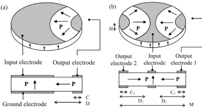
C P P Output electrode Input electrode D P (a) Ground electrode C1 P P Output electrode 1 Input electrode D1 P P C2 D2 (b) Output electrode 2 M H
Figure 1: The schematic views of (a) a disk-type single-input PT and (b) a disk-type dual-output PT.
It has to be emphasized that standard GA sometimes converges to local optimal points (non-optimal point). The elite GA, one of the variants of typical GAs, can ensure evolutionary processes converge to the global optimum. The basic principle of the elite GA is that the best chromosome of each generation is reserved as one of the chromosomes of the next children generation. Our preliminary study shows that when the elite GA was not employed, different optima were obtained even in the same search space. Therefore, in this work, we use the
we also parallelized the GA process using a PC cluster in order to speed up the optimization. By using the MPI libraries, the parallel calculations are implemented by dynamically balancing the workload in every generation and using the manager-worker paradigm [8].
2 OPTIMIZATION SCHEME
2.1 The Genetic Algorithms
GAs optimize a set of parameters (a chromosome) using adaptive search procedures based on the mechanisms of natural evolution. There are many GA evolution strategies which influence the convergence efficiency. In this work, the design goal is to maximize the efficiency under the constraint that the voltage gain is greater than 50 for igniting CCFL. Therefore, we formulate the cost function as two parts: the penalty function and the compromise function. The penalty function is defined as Equation (1):
) * * exp( 1 ) ( G G G G = + −α× − λ (1)
where G is a computed voltage gain, and G* is the
required voltage gain. α is a constant which
determines the steepness of the curve. In this work, α
is equal to 100. Obviously, when a chromosome
performs a voltage gain (G) lower than G*, the
penalty function will be much larger than 1, which eliminates the chromosome during the evolution process.
The compromise function calculates the distance between a solution and an ideal solution. The ideal solution is pre-defined by designers. A shorter distance indicates that a better solution is evaluated. The compromise function is defined as Equation (2):
* * ) ( e e e e r = − (2)
where e is a computed efficiency, and e* is the ideal
efficiency, which should be always equal to 100%. The cost function is the product of the penalty function and the compromise function, as shown in Equation (3):
r
⋅ =λ
cost (3)
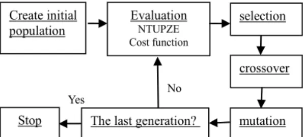
In this work, each of the design parameters will be encoded in a binary chromosome. A generation generates a new population from previous population. Therefore, the generation number is in fact the number of GA evolutions. Mutation is the occasional random alteration in a chromosome. Figure 2 shows the flowchart of the genetic algorithm. The GA parameters for each case presented in the work were the same. The initial population includes 40 chromosomes which are randomly created. The corresponding efficiency and voltage gain for each chromosome are evaluated. Based on the value of the cost function, 80% of chromosomes are selected for reproduction. A mutation ratio of 0.08 is used for the crossover operation. The selected chromosomes are randomly arranged in
created. Then the same procedure repeats until the design parameters converge.
No Yes
Create initial
population Evaluation NTUPZE Cost function
selection
crossover
mutation The last generation?
Stop
Figure 2: The flowchart of the Genetic algorithm.
2.2 Parallelization of GA
In our GA procedure, every chromosome requires an NTUPZE computation to evaluate the corresponding cost values. Computing 40 chromosomes for each generation require significant computational cost, so we employ a PC cluster to reduce total computation time. Through the evolution process, the chromosome population in a generation will converge. Considering the above reasons, the run-time allocation of tasks is employed. The parallel algorithm is based on manager-worker paradigm.
3 RESULTS AND DISCUSSIONS
3.1 Single-output PT with Crescent-Shaped Electrode
As shown in Figure 1, the single-output PT is a disk-type single-layered piezoelectric transformer with an asymmetric-crescent-shaped input electrode and an elliptically-shaped output electrode. The details of the device can be found in [7]. The design parameters are the
radius of the output section (D) and the radius of the
output electrode (C). Figure 3 shows comparison of
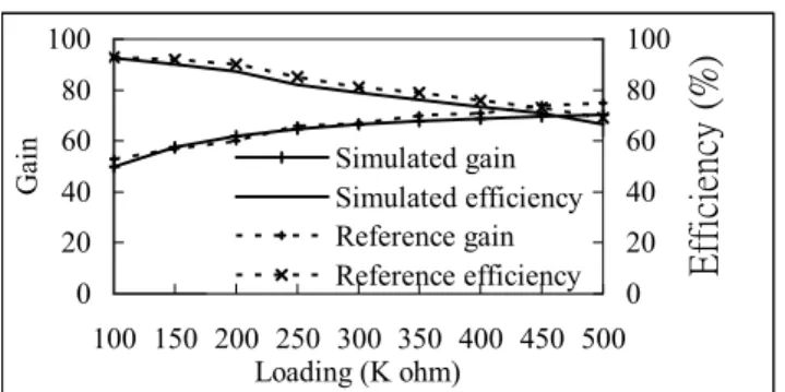
the simulated FEM results by using the NTUPZE and the measured results published in [7]. This figure verifies the accuracy of the NTUPZE.
In this case, G* is equal to 50. The dimensions of PT are 25.4 mm in diameter and 1.0 mm in thickness.
The resistive load is fixed at 100kΩ (the typical CCFL
impedance) during the GA optimization process. The design space is as follows: the output radius is from 5.7 mm to 13.7 mm and the electrode radius is from 1.7 mm to 8.7 mm. The material properties are listed in Appendix A.
Figure 4(a) shows the convergence performance of GA for this case. The optimized results for the radius of
the output section (D) and the radius of output electrode
( C ) is 12.70mm and 4.11mm, respectively. The corresponding voltage gain and efficiency are 53.8 and 91.9%, respectively. Also, as shown in Figure 5, we found that the higher the output section radius, the higher the efficiency. However, voltage gain is not necessarily higher. Figure 6(a) shows the deformed shape of the optimal design operating at resonance frequency. The GA parameters and the optimized results are listed in Table 1.
0 20 40 60 80 100 100 150 200 250 300 350 400 450 500 Loading (K ohm) Ga in 0 20 40 60 80 100
Efficien
cy
(%
)
Simulated gain Simulated efficiency Reference gain Reference efficiencyFigure 3: The verification of NTUPZE. Voltage gain and efficiency are as functions of load resistance.
0 0.5 1 1.5 2 0 20 40 Generation Co st min avg 0 1 2 3 4 0 20 40 Generation Co st min avg (a) (b) Figure 4: The convergence behaviors of the GA process
of (a) the single-output PT and (b) the dual-output PT.
0 10 20 30 40 50 60 70 80 90 6.2 7.45 9.45 11.2 12.95 13.45 Output section D(mm) Ga in 0 10 20 30 40 50 60 70 80 90 100 E ff ici ency (% ) Gain Efficiency(%)
Figure 5: The gain and the efficiency vs. the output section (D) for the single-output PT.
Type Parameters Single- output PT Dual- output PT Chromosome # 40 Generation # 40 Mutation ratio 0.08 Pick ratio 0.8 GA Parameters
Opt. Cost value 0.081 0.089 Device radius 12.7 mm 19.7 mm Output Sec. rad. 12.7 mm 12.4 mm Electrode radius 4.11 mm 5.4 mm Thickness 1 mm 1 mm Load Impedance 100 k ohm Max efficiency 91.9% 91.1% Dimensions & Performances of Opt. Devices Optimized gain 53.8 57.7
Table 1: The GA parameters and the optimized results of the two disk-type PT cases
(a) (b) Figure 6: The deformed shape of the optimal design operating at resonance frequency for (a) the single-output case and (b) the dual-output case.
3.2 Dual-output PT with Crescent-Shaped Electrodes
The schematic of the PT with dual outputs is shown in Figure 1. The poling directions and the design of the disk-type dual-output PT with crescent-shaped electrodes are similar to those of the single-output PT. In order to ensure the performances for both outputs are the same, a symmetric design is employed. In this case, there are
four design parameters: the radius (D) of the two output
sections, the radius (C) of the two output electrodes, the
radius (M ) of the device structure and the thickness (H)
of the device. Again, the design goal is to maximize the efficiency for both outputs under the constraint that the voltage gain has to be greater than 50 in order to meet the requirement of igniting CCFL.
The material properties are the same as those of the single-output PT. The resistive loads connected on the
two output electrodes are 100kΩ. The design space is
as follows: the output radius is from 4 mm to 12 mm, the electrode radius is from 2 mm to 8 mm, the device radius is from 10 mm to 20 mm, the device thickness is from 1 mm to 3 mm. The resolution of the genes is 5 bits. Figure 4(b) shows the GA convergence behavior of this
case. The optimized D, C , M, and H are 12.40
mm, 5.43 mm , 19.69 mm, and 1 mm, respectively. The corresponding voltage gains for both outputs are 57.5. Also, the corresponding efficiencies for both outputs are 91.1%. Table 1 summarizes these results. The characteristics of the optimal PT with different
loading
R
L are shown in Figure 7. Obviously, thegains increase with the load impedance. However, the efficiency is less than 90% as the load impedance is
larger than 100
k
Ω
. Figure 6(b) shows the deformedshape of the optimal design operating at resonance frequency. Figure 8 shows the benchmarks of the parallelized computations for the dual-output case. There are eight computers in our PC cluster. One of the computers serves as the manager. Each node is equipped with an Intel Pentium 4 CPU 3.0 GHz and 1GB memory. These nodes are interconnected through a Gigabit Ethernet network. The speedup and the efficiency for the parallel computation are defined as Equations (4) and (5). T(1) and T(NP) represent the
execution time for 1 and Np nodes, respectively.
) 1 (
% 100 × = p parallel N Speedup E (5)
As shown in Figure 8, the more computers are used, the less computation time is needed. However, the
computation efficiency ( Eparallel ) might not be
proportional to the number of computer nodes (the workers) when more PC nodes are used. It is because the total number of chromosomes which actually require the NTUPZE computations might be fewer than the computer nodes when the GA process is approaching convergence. 0 20 40 60 80 100 120 140 160 1 4 7 10 40 70 100 400
Load Impedance (K ohm)
Ga in 0 10 20 30 40 50 60 70 80 90 100 E ff ici en cy ( % ) Voltage Gain Efficiency(%)
Figure 7: Load resistance dependence of the voltage gains and the efficiencies of a dual output PT.
0 0.1 0.2 0.3 0.4 0.5 0.6 0.7 0.8 0.9 1 1 2 3 4 5 6 7 Np 0 1 2 3 4 5 6 7 8 Efficiency Speedup Figure 8: The benchmarks of the parallelized GA computations for the dual-output case.
4 CONCLUSIONS
In this work, the optimizations of two disk-type piezoelectric transformers (PTs) using genetic algorithm is presented. One of the PTs has single output electrode with crescent-shaped input electrodes, and the other disk-type PT has dual output electrodes with elliptically-shaped output electrodes. The dimensions of the output sections, the output electrode, and the device structure are the design parameters. The maximum efficiency and the required voltage gain to ignite CCFL are the design goals and the design constraint, respectively. The simulations were preformed by using the finite element solver, NTUPZE. The results were also verified with measured data. A parallel computation platform using a PC cluster is also implemented in order to speed up computational time. Benchmark results of the parallelized genetic algorithm
process are also presented. The characteristics of the optimal designs with different loads are also estimated by the NTUPZE. The voltage gain of the optimal PT with single output electrode is above 50, which is sufficient to ignite CCFLs. The efficiency of the optimal PT with single output electrode is above 90%. The optimized dual-output PT, which can ignite 2 CCFLs simultaneously, also gives sufficient voltage gains of greater than 57 for both output electrodes.
REFERENCES
[1] C. A. Rosen, “Solid State Magnetic and Dielectric Devices,” John Wiley & Sons, New York, 1st ed., Chap. 5, pp.170, 1959.
[2] H. W. Joo, C. H. Lee, J. S. Rho and H. K. Jung, “Identification of Material Constants for Piezoelectric Transformers by Three-Dimensional, Finite-Element Method and a Design-Sensitivity Method,” IEEE Transactions On Ultrasonics, Ferroelectrics, And Frequency Control, Vol. 50, No. 8, August 2003.
[3] J. Weisman, “Introduction to Optimization Theory,” Prentice-Hall, Inc., 1973.
[4] E. M. Baker, W. Huang and D. Y. Chen, “Radial mode piezoelectric transformer design for fluorescent lamp ballast applications,” IEEE Transactions On Power Electronics, Vol. 20, No. 5, September 2005.
[5] J. M. Seo, H. W. Joo and H. K. Jung, “Optimal design of piezoelectric transformer for high efficiency and high power density,” Sensors and Actuators A 121 (2005) 520-526.
[6] Y. M. Chen, “The Modeling and Simulation of the Piezoelectric Transformers by the finite element method”, M. S. Dissertation, Department of Mechanical Engineering, National Taiwan University, 2004.
[7] B. Koc, Y. Gao and K. Uchino, “Design of a Circular Piezoelectric Transformer with Crescent-Shaped Input Electrodes,” Jpn. J. Appl. Phys. Vol. 42 pp.509-514, 2003.
[8]
M. J. Quinn, “Parallel Programming in C
with MPI and OpenMP,” McGraw-Hill,
2003.
APPENDIX A
3 7500 m kg = ρ [ ] 2 10 10 10 10 10 10 10 10 10 10 10 10 10 0 . 3 0 0 0 0 0 0 10 6 . 2 0 0 0 0 0 0 10 6 . 2 0 0 0 0 0 0 10 5 . 11 10 3 . 7 10 3 . 7 0 0 0 10 3 . 7 10 0 . 14 10 1 . 7 0 0 0 10 3 . 7 10 1 . 7 10 0 . 14 m N C ⎥ ⎥ ⎥ ⎥ ⎥ ⎥ ⎥ ⎥ ⎦ ⎤ ⎢ ⎢ ⎢ ⎢ ⎢ ⎢ ⎢ ⎢ ⎣ ⎡ × × × × × × × × × × × × = [ ] 2 0 0 0 1 . 14 1 . 4 1 . 4 0 0 5 . 10 0 0 0 0 5 . 10 0 0 0 0 m C e ⎥ ⎥ ⎥ ⎦ ⎤ ⎢ ⎢ ⎢ ⎣ ⎡ − − =[ ]
Fm ⎥ ⎥ ⎥ ⎦ ⎤ ⎢ ⎢ ⎢ ⎣ ⎡ × × × = − − − 9 9 9 10 841 . 5 0 0 0 10 124 . 7 0 0 0 10 124 . 7 εResults
Implementation
Piezoelectric transformers
Piezoelectric transformers (PT), which were proposed in 1954 by Rosen,
step up or step down input voltages by electrical/mechanical/electrical conversion. Piezoelectric transformers have been proved to be promising alternatives for magnetic transformers because they have several advantages, such as low profile, high efficiency (low loss), no
electromagnetic radiation, nonflammable, low harmonic current noise, low temperature rise, and so on.
Methods
Optimization of Disk-type Piezoelectric Transformers
Chi-Wei Kuo, Chia-Yu Kang, Ying-Yin Huang, Chih-Kung Lee* and Yao-Joe Yang
Department of Mechanical Engineering, *Institute of Applied Mechanics
National Taiwan University, Taipei, Taiwan, ROC
Genetic Algorithm
The GA procedure consists of the following components: a genetic
representation of solutions to the problem, a way to create an initial
population of solutions, an evaluation function rating solutions, a reproduction step, and a mutation step.
No Yes
Create initial
population Evaluation NTUPZE Cost function
selection
crossover
mutation The last generation?
Stop
The flowchart of the GA algorithm
Elite GA
One of the variants of typical
GAs, which can ensure evolutionary processes converge to the global optimum .
The best chromosome of
each generation is reserved as one of the chromosomes of next children generation.
Introduction
GA has the following characteristics.
GA works with a coding of the parameter set rather than the parameters
themselves.
GA searches from a population of points rather than a single point.
GA use payoff information (objective function) rather than derivatives or
other auxiliary knowledge.
GA uses the probabilistic transition rules rather than the deterministic rule.
C P P Output electrode Input electrode D P (a) Ground electrode C1 P P Output electrode 1 Input electrode D1 P P C2 D2 (b) Output electrode 2 M H
The schematic views of (a) a disk-type single-input PT with crescent-shaped electrodes and (b) a disk-type dual-output PT with crescent-shaped electrodes.
Assigning cost function
The design goal is to maximize the efficiency under the constraint that the
voltage gain is greater than 50 for igniting CCFL. Therefore, we formulate the cost function as two parts:
The penalty function
The compromise function
The cost function is the product of the penalty function and the compromise
function ) * * exp( 1 ) ( G G G G = + −α× − λ * * ) ( e e e e r = − r ⋅ =λ cost •e : computed efficiency •e* : ideal efficiency
•G : computed voltage gain
•G*: required voltage gain
• : constant which determines the steepness of the curve
α
All of the optimization process is implemented in C++
Including the FEM solver NTUPZE and the GA procedure.
Single-output PT with Crescent-Shaped Electrode
Dual-output PT with Crescent-Shaped Electrodes
Type
Parameters Single- output PT Dual- output PT
Chromosome # 40 Generation # 40 Mutation ratio 0.08 Pick ratio 0.8 GA Parameters
Opt. Cost value 0.081 0.089
Device radius 12.7 mm 19.7 mm
Output Sec. rad. 12.7 mm 12.4 mm
Electrode radius 4.11 mm 5.4 mm
Thickness 1 mm 1 mm
Load Impedance 100 k ohm
Max efficiency 91.9% 91.1% Dimensions & Performances of Opt. Devices Optimized gain 53.8 57.7
Table 1: The GA parameters and the optimized results of the two disk-type PT cases
A disk-type single-layered
piezoelectric transformer with an asymmetric-crescent-shaped input electrode and an elliptically-shaped output electrode.
The design space is as
follows: the output radius is from 5.7 mm to 13.7 mm and the electrode radius is from 1.7 mm to 8.7 mm. 0 10 20 30 40 50 60 70 80 90 6.2 7.45 9.45 11.2 12.9513.45 Output section D(mm) Ga in 0 10 20 30 40 50 60 70 80 90 100 Ef fi ci en cy ( % ) Gain Efficiency(%) 4 0 6 0 8 0 1 0 0 1 2 0 1 4 0 1 6 0 Gai n 2 0 3 0 4 0 5 0 6 0 7 0 8 0 9 0 1 0 0 E ff ici enc y (% ) V o lta g e G a i n E f f i c ie n c y ( % ) 0 20 40 60 80 100 100 150 200 250 300 350 400 450 500 Loading (K ohm) Ga in 0 20 40 60 80 100 Ef fi ci en cy ( % ) Simulated gain Simulated efficiency Reference gain Reference efficiency 0 0.5 1 1.5 2 0 20 40 Generation Co st min avg 0 1 2 3 4 0 20 40 Generation Co st min avg (a) (b)
The deformed shape of the single-output PT
The gain and the efficiency vs. the output section (D) for the single-output PT.
The verification of NTUPZE. Voltage gain and efficiency are as functions of load resistance.
The convergence behaviors of the GA process of (a) the single-output PT and (b) the dual-output PT 0.2 0.3 0.4 0.5 0.6 0.7 0.8 0.9 1 1 2 3 4 5 6 7 8 Efficiency Speedup
Parallelized the GA process using a PC cluster
The more computers are used, the less computation time is needed.
The poling directions and the design of
the disk-type dual-output PT with crescent-shaped electrodes are similar to those of the single-output PT
The design space is as follows: the
output radius is from 4 mm to 12 mm, the electrode radius is from 2 mm to 8 mm, the device radius is from 10 mm to 20 mm, the device thickness is from 1 mm to 3 mm.