474 IEEE TRANSACTIONS ON VEHICULAR TECHNOLOGY, VOL. 43, NO. 3, AUGUST 1994
Digital Tanlock
Loop for Tracking
r/4-DQPSK Signals in Digital Cellular Radio
Che-Ho Wei, Senior Member, IEEE, and Wen-Jiang ChenAbstruct- A digital tanlock loop (DTL) is a nonuniform- sampling digital phase-locked loop (DPLL) whose ,phase error detector, using the tan-'[.] function with in-phase and quadra- ture samples of incoming signal, has a linear characteristic with a period of 27r. In this paper, we study the application of an N-
phase DTL in digital cellular radio with d4-DQPSK modulation. The performance degradation due to fading effect is investigated in terms of bit error rate and steady state phase error variance by computer simulation. It is shown that, in the digital cellular radio system, the performances on both bit error rate and phase error variance using DTL are far better than that using the traditional digital N-phase I-Q loop.
I. INTRODUCTION
INCE THE early 1970's, a variety of digital phase-locked
S
loops (DPLL's) have been proposed and analyzed [I]. A continuous wave (CW) DPLL that tracks the positive- going zero crossings of the incoming signal and results in nonuniform sampling was first introduced by Gill and Gupta [2], [3]. The behavior of this DPLL is characterized by a sinusoidal nonlinear difference equation in the phase error process. Recently, a new type of nonuniform-sampling DPLL, called the digital tanlock loop (DTL), as shown in Fig. 1, was introduced by Lee and Un [4]. The main feature of this loop is that the phase error detector has a tan-'[.] function and, therefore, has a linear characteristic in the modulo-2.rr sense. Accordingly, the DTL can be characterized by a linear difference equation, thereby making it possible to analyze the system easily without approximation of nonlinearity. It has several attractive features in comparison to the conventional DPLL's with sinusoidal phase characteristics. First, the DTL has wider lock range and less steady state phase error for the first-order loop in the absence of noise. Second, the DTL can be locked independently of initial phase error for some region of parameters. Third, the DTL is insensitive to the variation of the input signal power and, thus, requires no automatic gain control circuits.An N-phase DTL has been introduced by Kin, Un and Lee [5] for tracking N-ary suppressed-carrier phase-shift keying (PSK) signal. The N-phase DTL is also characterized by linear difference equation and gives the same advantages over the traditional digital N-phase
I-&
loop [I]. Furthermore, withManuscript received November 18, 1992; revised February 10, 1993 and July 30, 1993. This work was supported by the National Science Council of
Republic of China, under grant NSC81-0404-E009-009.
The authors are with the Institute of Electronics and Center for Telecommu- nications Research, National Chiao Tung University, Hsinchu, Taiwan, R.O.C.
IEEE Log Number 9215553.
1 T
Fig. 1. Block diagram of DTL.
the N-phase DTL, we can accomplish demodulation directly on the phases obtained at the phase detector.
In cellular radio over fading channels, the received signal is not only corrupted by the AWGN noise, but also randomly perturbed in both amplitude and phase. The statistical analysis of DPLL in fading channels was first introduced by Varanasi and Gupta [6]. Elnoubi and Gupta [7] studied the performance of a first-order DPLL in mobile radio channels by solving the Chapman-Kolmogorov (C-K) equation and obtained the probability density function (pdf) of the steady-state phase error.
In this paper, we study the application of the N-phase DTL in digital cellular radio with ?r/4-DQPSK modulation. The performance degradation due to the fading effect is investigated in terms of the phase error variance and the bit error probability by computer simulation. A performance comparison is made between the N-phase DTL and the digital N-phase
I-&
loop. In addition, the effect of quantization on the performance of the N-phase DTL is investigated by simulation.11. THEORETICAL BACKGROUND
A. N-Phase Digital Tanlock Loop
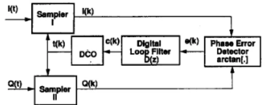
The N-phase DTL [5] that tracks the N-ary suppressed- canier PSK signal is diagrammed in Fig. 2. It is composed of two samplers, a phase error detector, a loop filter, and a digitally controlled oscillator (DCO). The samplers, controlled by the DCO, nonuniformly sample the in-phase and quadrature components I ( t ) and Q ( t ) of the input signal. The phase error detector of the N-phase DTL is composed of a tan-' [.] function, an N-times multiplier, and a modulo-27r device. The tan-' [.] operation can be performed by using a precalculated tan-'[.] table. As a result of using the tan-'[.] function, the characteristic of the phase error detector is linear in the
WE1 AND CHEN: DIGITAL TANLOCK LQOP FOR TRACKING ?r/+DQPSK SIGNALS 415
Fig. 2. Block diagram of the N-phase DTL ( F [ z ] =
-*
+
[(z+
*)modulo 2x1).modulo-2~/N sense. The N-times multiplier and the modulo- 2~ device are used to eliminate modulation from the N-ary
PSK signal.
The behavior of the loop depends largely upon the transfer function of the digital loop filter
D ( z ) .
For a second-order loop filter, the transfer function is given by D ( z ) = GI+
where G1 and G2 are positive constants. The output of the digital loop filter provides a control signal c ( k ) to the DCO for the next sampling operation. In the system considered here, the DCO provides the same sampling time to the two samplers. The time interval between the k-th and
( k
+
1)-th sampling instants is controlled by the phase detector output of the k-th sampling time passing through the digital loop filter.The in-phase and quadrature components of the mixed-down and bandpass-filtered N-ary signal at the input of the DTL,
I ( t ) and
Q ( t ) ,
can be written asI ( t ) =
a ( t )
cos[wet
+
@(t)
+
8 i ( t )+
6&(t)]+
w(t) (1)Q ( t )
=a ( t )
sin [wot+
@ ( t )
+
& ( t )
+
& h ( t ) ]+
G ( t ) (2)where
w(t) = f i [ N , ( t ) cos(w0t
+
& ( t ) )
-
N,(t) sin(w0t+
O ; ( t ) ) ](3)
and
a ( t )
and e&(t) denote, respectively, the amplitude and the phase random processes due to the fading channel. Also,&( t )(=
190+
A w. t ) ,
denotes an arbitrary constant phase I90 plus a phase deviation due to the frequency offset A w fromw g . N,(t) and N,(t) represent the quadrature components of
the bandlimited white Gaussian noise zu
( t )
with one-sided power spectral density No. The function G(t) denotes the noise process obtained by 90-degree phase-shifting the bandlimited noise w ( t ) . Also,@ ( t )
denotes a modulating data phase for nonretum-to-zero coding, that is,-03
@ ( t )
= @ k.
[ U ( t - kTs) - U ( t- (k
- 1)Ts)] (4) k = - mwhere u ( t ) is a unit-step function and Ts is the symbol period. For r/4-DQPSK modulation, @k is the information-bearing
phase having a value of 2 n ~ / N ( n = O , f l , f 2 , f 3 , f 4 ) during the k-th symbol interval and N is equal to 8 [8], [9].
The sampling interval ~ ( k ) of the DCO is controlled by the output c(
k
- 1) of the digital loop filter at the sampling instanlt ( k
-
l ) , and is given by~ ( k ) E t ( k )
-
t ( k-
1) = T-
~ ( k - 1) ( 5 )where T
e
= is the nominal sampling period of the DCO and m is a design parameter to give options in choosing the sampling period.Assuming that t ( 0 ) = 0, we have k - 1
t ( k ) =
kT
-
c ( j ) . ( 6 ) j = ONow, considering the case of m/N being an integer, the values of I ( t ) and Q ( t ) sampled at the k-th sampling instant t ( k ) may be written, respectively, as
I(k)
= a(k)cos[($(k)
+
@ k ]+
w ( k ) Q ( k ) = a ( k ) sin[($(k)
+
@ k ]+
G ( k )(7) (8)
where the phase error
($(k)
of the N-phaseDTL
is defined ask-1
4(k)
= @ i ( k )+
@ c h ( k ) - w0 c ( j ) - (9)j = O Then, the phase detector output e ( k ) is given by
e ( k ) = F [ 8 .
z(k)]
(10)where
F [ . ]
represents the function of modulo-2~ operation, i.e.,(11)
F ( x )
=
-T+
[(x
+
T) modulo 2x1 andB . Digital N-Phase I-Q Loop
The block diagram of the digital N-phase I-& loop is shown in Fig. 3 [l]. In fact, the digital N-phase I-& loop is a modified version of the conventional DPLL for tracking N - ary PSK signals. One may note that the structure of the digital N-phase I-Q loop is similar to that of the N-phase DTL, except the phase error detector. The phase error detector of the digital N-phase I-Q loop contains a 2-(%-') .Im[I(k)
+
j Q ( k ) I N operation. This operation involves a complex number multiplication of order N that is used to eliminate modulation from the ~ - a r y PSK signal. AS a result of using the 2-(+-').
Im[I(k)
+
j Q ( k ) l N function, the characteristic of the phase error detector is nonlinear in the modulo-2r/N sense, and thus, makes it difficult to analyze the loop exactly. Besides, the use of a complex number multiplier of order N also makes the hardware implementation complex and difficult compared to the N-phase DTL. Also, the data phase can not be extracted directly from the loop, as the case of the N-phase DTL, but must perform the tan-'(.] operation first on the in-phase416 IEEE TRANSACTIONS ON VEHICULAR TECHNOLOGY, VOL. 43, NO. 3, AUGUST 1994
1
I I
Fig. 3. Block diagram of the N-phase I-& loop.
Modulator Fading channel
Fig. 4. Block diagram of digital cellular radio system.
and quadrature components of the samplers outputs. Thus, the demodulation is more complex than the N-phase DTL.
The in-phase and quadrature components of the input signal at the IC-th sampling interval are also given by (7) and (8). The phase detector output for 7rI4-DQPSK signal can be expressed by
where the phase error + ( I C ) is also defined as (9).
HI. SIMULATION OF N-PHASE DIGITAL TANLOCK LOOP IN DIGITAL CELLULAR RADIO WITH 7rI4-DQPSK MODULATION
The block diagram of the system simulated is depicted in Fig. 4. In the simulation, the signal and noise specifications are given as:
1) Bit rate is 48 kb/s, therefore the symbol rate is 24
2) Nominal frequency of the carrier is 4 times the symbol 3) Bandwidth B of AWGN is 1.2/T and one-sided spectral 4) Doppler frequency shift is 30 Hz.
ksymbols/s. rate, i.e., 96 kHz.
density NO = [w/Hz].
A . Fading Channels
of additive white Gaussian noise can be represented as The signal passing through the fading channel in the absence
(14)
R(t) = a ( t ) sin [ w l t
+
&h(t)+
& ( t )
+
@ ( t ) ]
withe&)
= tan-' [A?::(
t )
]
where w1 is the carrier frequency, and XI and XQ are referred to as the in-phase and quadrature components, which are
Fig. 5. Model of .rr/4-DQPSK modulator.
assumed to be zero-mean, independent, stationary Gaussian random processes. Note that wg
=
w1 - W L O , where WLO isthe local oscillator output frequency.
When A is nonzero, the channel is a Rician fading channel. The average power of the received signal R(t) corresponding to the specular component is
A 2
[watts] and the power in each of the XI and XQ component is denoted by v;. The fading parameter is defined as the ratio of the average specular power to the fading powerA2
D-M E
-.
2 4
When A = 0, the channel is denoted as a Rayleigh fading channel. In practice, when
D X
is very small (less than 0.01), the channel can be treated as a Rayleigh channel. When D-Mis large (say 0.1-loo), the channel can be treated as a Rician channel. When D-M
>
100, the channel is essentially a nonfading channel.B . Modulation
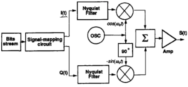
The block diagram of the modulator for the 7r/4-DQPSK signal is shown in Fig. 5. Let f ( t ) and Q(t) denote the un- filtered rectangular pulse of in-phase and- quadrature channels, respectively. The signal levels-Ik and Qk, which denote the pulse amplitude of I(t) and Q(t) for ICT
5 t
<
(IC+
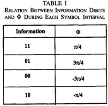
1)T, are determined by the previous signal levels and the current information symbol denoted by the phase shift @ k.
The phase shift @ k is determined by the transmitted dibit as shown in Table I. The relation between @ k and the transmitted dibit can be expressed as [9]-
-I k = 4 - 1 cos@k - Qk-1 S h @ k Qk = I k - 1 Sin @ k+
Qk-1 COS @k. (164 ( 16b) The transmitted phase falls into one of two sets of QPSK in tum. Between two successive symbol periods, the possible phase shifts can only be f z / 4 and f37r/4.C . Demodulation
Since the data phase @ k is extracted from the phase detector output of the N-phase DTL directly, demodulation can be accomplished easily. After the obtained data phase @ k having been detected as one of the possible values & y ( n =
WE1 AND CHEN: DIGITAL TANLOCK LOOP FOR TRACKING ?r/&DQPSK SIGNALS
word length (bW
411
variance of ek stardand deviation of ek 0.13031 0.01698
TABLE I
RELATION BEIWEEN INFORMATION D m m AND DURING EACH SYMBOL INTERVAL
Information 0.13212 0.1 3395 16 12 0.36348 0.36476
0 , 1 , 2 , 3 , 4 ) , the transmitted information phase can be deter- mined by the difference of the current value and previous one, i.e., @k - Under the noiseless condition, it can only be f r / 4 or f37r/4. Thus, the transmitted dibits are
decided according to the same mapping rule as Table I and the demodulation process is completed.
10 8 6 4
Iv. SIMULATION mSULTS AND DISCUSSION
In this section, we give the simulation results and discuss several aspects regarding the N-phase DTL and make a performance comparison between the N-phase DTL and the digital N-phase I-& loop. The sampling operation of the N - phase DTL is controlled directly by the DCO. The nominal sampling frequency f n is defined as the inverse of the nominal
sampling period T
0.13351 0.36539
0.15066 0.38815
0.26633 0.51607
0.82360 0.90684
A. Finite Wordlength Effects of the N-Phase DTL Implementation
We can consider two kinds of wordlengths in implementing the N-phase DTL: the wordlength Nl of the A/D converter output after the sample-and-hold circuit, and the wordlength N2 of phase ~ ( k ) and e ( k ) .
The wordlength N1 of the A/D converter output directly affects the memory size of the table which is used for performing the tan-'[.] operation. If we use one bit of N1 as a sign bit, the memory size of the tan-l[.] operation required becomes about 2N1-1.N2 b, since the output Zk of the tan-'[.] operation is represented by N2 b.
In Table 11, we show the variance and standard deviation of e ( k ) obtained from computer simulation in the Rayleigh fading channel for various wordlengths. The ratio of average symbol energy to AWGN mean power, &/No used in this simulation have been chosen arbitrarily. In the simulation, we used the same wordlength for N1 and N2. The first row in the table shows the simulation result for the case of infinite precision. This simulation result suggests a guideline for hardware design of an N-phase DTL.
10
B . Hardware implementation Consideration
The functional block diagram of the N-phase DTL is shown in Fig. 6 [l], [12]. The phase error detector is composed of
4 4
TABLE II
VARIANCE AND STANDARD DEVIATION OF e k AS A F U " 0 N OF WORD LENGTH
c
Fig. 6. signal.
Functional block diagram of the N-phase DTL for T/~-DQPSK
a tan-'[.] function, an N-times multiplier, and a modulo-
27r device. The tan-l[.] operation can be implemented by an ROM using table lookup method. The N-multiplication function can be implemented by a 3-b shifter since N is 23
for 7r/4-DQPSK signal, while the digital N-phase
I-&
loop requires a complex number multiplier of order N. For largeN, the use of a complex number multiplier would be difficult due to the finite wordlength effect.
C . Pe$ormance of N-Phase DTL in Fading Channels Here we discuss the performance of the N-phase DTL in the Rayleigh fading and Rician fading channels, and compare it with the digital N-phase
I-&
loop, in terms of phase error variance and bit error probability.1) Phase Error variance: The phase error variances of the N-phase DTL and the digital N-phase
I-&
loop are calculated by0; = E { + 2 ( k ) }
-
P{4(~)1I2
(18) whereE{
.} denotes the expectation value of a random process, and$(k)
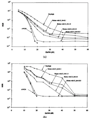
is the phase error of the loop defined in (9). Fig. 7 shows the simulated phase error variance as a function of &/No (indB)
in Rician fading channel for D-M of 10, 1, 0.1, and Rayleigh fading channel, respectively. It is found that the N-phase DTL has a better performance than the digital N-phaseI-&
loop for having the less phase error variance. It is also seen478 IEEE TRANSAmONS ON VEHICULAR TECHNOLOGY, VOL. 43, NO. 3, AUGUST 1994
10' loo .
/wwb I
Fig. 7. (a) Variance of e.+ for the N-phase DTL in the fading channel. (b) Variance of e k for the N-phase IQL in the fading channel.
Fig. 8. (a) BER for the N-phase DTL in the fading channel. (b) BER for
the N-phase IQL in the fading channel.
from Fig. 7 that, as the effect of the fading increases, the difference between the N-phase DTL and the digital N-phase I-& loop becomes more significant.
2) Bit Error Probability: The simulation results of the bit error probability of the N-phase DTL and the digital N - phase
I-&
loop are given in Fig. 8. They are plotted as a function of Eb/N, (in dB) in Rician fading channel with D-M equal to 10, 1, 0.1, and Rayleigh fading channel, respectively. It can be seen from the figures that the bit error rate of the N-phase DTL is much smaller than that of the digital N-phaseI-&
loop. When the effect of fading increases, the bit error rate of the N - phase DTL increases sharply. This results mainly from the fact that the digital N-phaseI-&
loop is affected by variation of signal power. The effect of fading on the amplitude of the incoming signal severely affects the loop tracking performance. For r/4-DQPSK signals, the phase detector of the digital N-phaseI-&
loop is a complex multiplier of order 8. This further worsens the loop performance when the fading effect is severe. While the N-phase DTL is less affected by the signal power, thus have much better BER performance.N-phase DTL is that the phase error has linear characteristics in the modulo-2~/N sense as a result of using a new type of phase detector.
The performances of the N-phase DTL and the digital N - phase
I-&
loop have been analyzed in detail. Also, the effect of finite wordlength on the performance of the N-phase DTL has been investigated by computer simulation. In addition, the performance of the N-phase DTL has been compared to that of the digital N-phaseI-&
loop. The N-phase DTL has several significant advantages over the digital N-phaseI-&
loop. First, for the first-order loop the N-phase DTL has wider locking range and less steady-state phase error. Second, the N-phase DTL is simpler to be implemented. Third, unlike the digital N-phaseI-&
loop, we have a simple demodulation scheme with the N-phase DTL. Fourth, we can easily analyze the N-phase DTL without approximating the sinusoidal nonlinearity, as usually done in the case of the digital N-phaseI-&
loop. Since the N-phase DTL is not affected by the variation of signal power, its locking conditions are independent of the incoming signal power. Thus, it achieves less phase error variance and smaller bit error probability. These results have been verified by computer simulations.V. CONCLUSION
In this paper, the applications of the N-phase DTL and the digital N-phase
I-&
loop in digital cellular radio with ~ / 4 - DQPSK modulation have been studied. The main feature of theACKNOWLEDGMENT
The authors would like to thank the reviewers for their valuable suggestions.
WE1 AND CHEN: DIGITAL TANLOCK LOOP FOR TRACKING n/&DQPSK SIGNALS
REFERENCES
[ l ] W. C. Lindsey and C. M. Chie, “A survey of digital phase-locked loops,”
Proc. ZEEE, v01. 69, pp. 410-431, Apr. 1981.
[2] G. S. Gill and S. C. Gupta, “First-order discrete phase-locked loop with applications to demodulation of angle-modulated carrier,” ZEEE Trans. Commun., vol. COM-20, pp. 454-462, June 1972.
[3] A. Weinberg and B. Liu, “Discrete time analysis of nonuniform sam-
pling first- and second-order digital phase-locked loops,” ZEEE Trans. Commun., vol. COM-22, pp. 123-137, Feb. 1974.
[4] J. C. Lee and C. K. Un, “Performance analysis of digital tanlock loop,” ZEEE Trans. Commun., vol. COM-30, pp. 2398-2411, Oct. 1982. [5] H. J. Kin, C. K. Un and J. C. Lee, “The N-phase digital tanlock loop for
tracking suppressedcanier N-ary PSK signals,” ZEEE Trans. Commun.,
[6] S. Varanasi and S. C. Gupta, “Statistical analysis of digital phase-locked loops in fading channels,” ZEEE Trans. Aerosp. Electron. Sysr., vol. [7] S. M. Elnoubi and S. C. Gupta, “Performance of first order digital phase- locked loops in mobile radio channels,” ZEEE Trans. Commun., vol. COM-33, pp. 450-456, May 1985.
181 F. Adachi and K. Ohno, “Postdetection selection diversity reception with correlated, unequal average power Rayleigh fading signals for 7r/4-shift QDPSK mobile radi0,”ZEEE Trans. Veeh. Technol., vol. 41, pp. 199-210,
May 1992.
[9] C.-L. Liu and K. Feher, “Non-coherent */4-QPSK in an AWGN-CCI combined interference environment,” in Proc. ZEEE 39th Veh. Technof. Conf., San Francisco, CA, May 1989, pp. 83-94.
[lo] H. C. Osbome, “Stability analysis of an Nth power digital phase-locked loop-Part I: First-order DPLL,” ZEEE Trans. Commun., vol. COM-28, pp. 1343-1354, Aug. 1980.
[ l l ] H. C. Osbome, “Stability analysis of an Nth power digital phase-locked
loop-Part II: Second- and third-order DPLL’s,” IEEE Trans. Commun.,
[12] S. Ono, T. Aoyama, M. Hagiwara and M. Nakagawa, “Implementation of a new type DSP PLL using high performance DSP DSSP-I,” in Proc.
ZEEE ZCASSP‘86, Tokyo, Japan, April 1986, pp. 2195-2198.
V O ~ . COM-33, pp. 904-909, Sept. 1985.
AES-20, pp. 682693, NOV. 1984.
V O ~ . COM-28, pp. 1355-1364, Aug. 1980.
419
Che-Ho Wei (S’73-M’7&M’7%SM’87) was bom in Taiwan in 1946. He received the B.S. and M.S. degrees in electronic engineering from National Chiao Tung University (NCTU), Hsinchu, Taiwan, R.O.C., in 1968 and 1970, respectively, and the Ph.D. degree in electrical engineering from the University of Washington, Seattle, in 1976.
From 1976 to 1979, he was an Associate Pro- fessor at NCTU, where he is now a Professor in the Department of Electronics Engineering and the Institute of Electronics. From 1979 to 1982, he was the Engineering Manager of Wang Industrial Company in Taipei, Taiwan. He was the Chairman of the Department of Electronics Engineering of NCTU from 1982 to 1986 and Director of the Institute of Electronics from 1984 to 1989. He was on leave at the Ministry of Education and served as the Director of Advisory Office from September 1990 to July 1992. His research interests include digital communications and signal processing, and related
VLSI circuits design.
Dr. Wei was the founding chairman of both the IEEE Circuits and Systems Society and E E E Communications Society chapters in Taipei. He is the
Chairman of IEEE Taipei section, 1993-1994. He received the Outstanding Research Award in 1987-1989 and the Distinguished Research Award in 1990 and 1992 from the National Science Council, Taiwan, R.O.C.
Wen-Jiang Chen was bom in Taiwan in 1967. He received the B.S. and M.S. degrees in electronic engineering from National Chiao Tung University, Hsinchu, Taiwan, R.O.C., in 1990 and 1992, respec- tively.
He is now with Computer and Communication Laboratory, Industrial Technology Research Insti- tute (ITRI) in Hsinchu, Taiwan. His research inter- ests are in the areas of wireless communications and digital signal processing.
![Fig. 2. Block diagram of the N-phase DTL ( F [ z ] = -*](https://thumb-ap.123doks.com/thumbv2/9libinfo/7580863.126435/2.922.123.466.98.246/fig-block-diagram-n-phase-dtl-f-z.webp)