818 IEEE TRANSACTIONS ON ELECTRON DEVICES, VOL. ED-28, NO. I , JULY 1981
Modeling and Optimization of Monolithic
Polycrystalline Silicon Resistors
Absfract-The processing parameters of monolithic polycrystalline silicon resistors are examined, and the effect of grain size on the sensi- tivity of polysilicon resistivity versus doping concentration is studied theoreticay and experimentally. Because existing models for poly- silicon do not accurately predict resistivity dependence on doping con- centration as grain size increases above 600 A, a modified trapping
model for polysilicon with different grain sizes and under various ap- plied biases is introduced. Good agreement between theory and experi- ments demonstrates that an increase in grain size from 230 t o 1220 A
drastically reduces the sensitivity of polysilicon resistivity t o doping levels by two orders of magnitude. Such an increase is achieved by modifications of the integrated-circuit processes. Design criteria for the optimization of monolithic polysilicon resistors have also been established based on resistivity control, thermal properties, and device geometry.
SYMBOLS Cross-section area of resistor (cm’). Impurity (acceptor) level (ev).
Activation energy of resistivity to l / k T (eV). Fermi energy level (ev).
Energy band gap (ev).
Intrinsic Fermi level referred to Eio(eV). Intrinsic Fermi level at center of the grain (ev). Grain-boundary trapping state energy referred to
Trapping state energy referred to Ei at grain boundary
Planck’s constant. Current (A).
Saturation current (A). Current density (A/cm2). Boltzmann’s constant. Grain size (cm).
half-width of crystallite neutral region (cm). Electron effective mass (kg).
Hole effective mass (kg). Doping concentration (cm-’).
Ionized impurity concentration (cm-’).
Eio (eV>*
( e V .
Manuscript received September 16, 1980; revised December 1, 1980. This research was sponsored by the Defense Advanced Research Proiects Agency and monitored by the Office of Naval Research under Coniract MDA 903-79-C-0680.
N.C.C. Lu, L. Gerzberg, and J. D. Meindl are with the Integrated Cir- C-Y. Lu is with the Institute of Electronics, National Chiao-Tung cuits Laboratory, Stanford University, Stanford, CA 94305. University, Hsin-Chu, Taiwan, Republic of China.
Doping concentration below which grains are com-
Number of grains between resistor contacts. Intrinsic carrier concentration (cm-’). Hole concentration (cm-’)>.
Hole concentration in neutral region or at center of the grain ( ~ m - ~ ) .
Average carrier (hole) concentration (cm-’). Elementary charge.
Grain-boundary trapping state density (cm-’). Effective (or ionized) trapping state demity (cm-’). Resistance
(a).
Absolute temperature (K).
Applied voltage between resistor contacts (V). Built-in potential barrier height (V).
Applied voltage across grain-boundary barriers (V). Applied voltage across crystallite neutral region (V). Applied voltage across each grain (V).
Width of depletion region (cm). Grain-boundary thickness (cm). Single-crystal silicon permittivity. Polysilicon resistivity
(a
* cm).Barrier resistivity
(a
cm).Crystallite bulk resistivity
(a
cm). Grain-boundary resistivity(a
* cm).Polysilicon effective mobility [cm2/(V s)]
.
Electron mobility of single-crystal silicon [cm’/(V s)]
.
Hole mobility of single-crystal silicon [cm’/(V * s)].
pletely depleted (cm-’).
I. INTRODUCTION
P
OLYCRYSTALLINE silicon (polysilicon) has been stud- ied for many years and has found an increasing number of recent applications [ l ] in solar cells, integrated-circuit elements such as silicon-gate MOS devices, interconnections, passivation or isolation layers, monolithic distributed RC fil-ters, and high-value resistors. Polysilicon resistors are impor- tant for integrated circuits for the following reasons:
They are compatible with such monolithic silicon technol- ogies as MOS or bipolar (BJT) processes [2].
Resistance can be adjusted through several decades by ion implantation where the lightly doped material has a sheet resistance as high as that of pure intrinsic single-crystal silicon especially required in low-power circuits.
Resistors top-deposited on the field oxide of MOS IC’s or on
LU e t al.: MODELING AND OPTIMIZATION OF RESISTORS 819
DOPING CONCENTRATION I~rn-~)
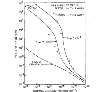
Fig. 1. Measured and theoretical resistivities versus doping concentra- tions a t room temperature for polysilicon with various grain sizes and for single-crystal silicon.
the isolation region of bipolar transistors require no extra area compared to the large space occupied by diffused or ion- implanted resistors.
Because they are isolated by a thick oxide, resistance is much less dependent on substrate bias, and parasitic capaci- tance i s smaller than that resulting from junction isolation in diffused or implanted resistors.
Their negative temperature coefficient can compensate for the temperature dependence of leakage or subthreshold cur- rent in active devices [3].
Their linearity is good for a common electric field where sheet resistance ranges as high as gigaohm per square; this is in contrast to the much lower linearity and less controllability of all other monolithic resistors [2].
The following problems are encountered when employing polysilicon for monolithic resistors.
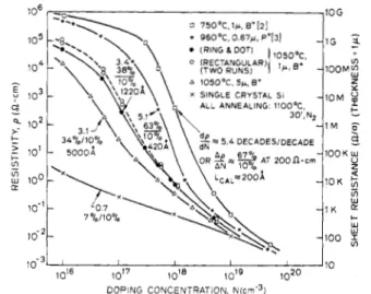
The sensitivity of polysilicon resistivity to doping concentra- tion is very large, especially in the high-resistivity range; for example, over the doping level of 5 X lo" t o 5 X 10l8 cmm3, a resistivity change of approximately five decades has been observed (Fig. 1) [4].
The structure of polysilicon and grain size are sensitive t o thermal processing steps; in addition, implanted arsenic dopants segregate to the grain boundaries in quantities that are depen- dent on annealing temperatures [5]. These cause poor resis- tivity control and instability in doped polysilicon [2], [6].
Polysilicon shows a very large temperature coefficient, espe- cially in lightly doped samples. For example, a sheet resistance of 1 GS2/n at 25°C drops three decades when the temperature is elevated t o 160°C [4].
To resolve these problems, this paper introduces a new modified trapping model for monolithic palysilicon resistors with small and large grain sizes and applies it to device analysis and optimization. Processing parameters are selected t o ensure good control and reproducibility of the material properties.
Experimental procedures are described. Theoretical and exper- imental results are compared, and the validity of this quantita- tive model is demonstrated. Based on this model, design criteria (such as resistivity control, thermal properties, and de- vice geometry) are established for monolithic polysilicon resistors.
A . Processing Parameters
By comparing the sharp change in resistivity versus doping concentration (pversusN) in polysilicon to the gradual change in single-crystal silicon, resistivity dependence on the doping level in polysilicon is expected to approach that of single- crystal silicon and thereby demonstrate lower sensitivity [2], [7] as grain size increases. High deposition temperature or the deposition of thick film can .result in a large grain size; how- ever, acceptable surface roughness, lithography resolution, and smaller device geometry limit the maximum size. Other device- processing constraints dictate the highest deposition tempera- ture. This paper investigates the effect of grain size on the p versus N curve based on published data [4], [8] for 1 .O- and
0.67-pm-thick polysilicon layers with grain sizes of 230 and 420.4 and deposition temperatures of 750" and 960"C, respectively, and on data obtained from this work for 1 .O- and 5.0-pm-thick fdms deposited at 1050°C and with grain sizes from 0.1 to 1.0 pm.
' The columnar structure of polysilicon increases the diffusivity of dopants to a much higher degree than does single-crystal silicon [9]. Because the diffusion process strongly depends on grain structure and deposition temperature, doping polysilicon with a diffusion source is difficult to control. Better control is achieved by dopant ion implantation [4] through an oxide layer on top of the polysilicon to avoid loss of dopants during subsequent thermal steps; high-temperature postimplantation annealing was used to activate and redistribute them uniformly throughout the film immediately after implantation. It was also observed that the sensitivity of grain size t o annealing temperature is reduced substantially at 1000°C or higher [ l o ] Grain growth is also related to deposition temperature; the initial size of polysilicon deposited at 600" t o 900°C is small, and significant changes in structure and dimensions occur during subsequent higher thermal steps [8]. On the other hand, a high deposition temperature produces relatively large grains that are unlikely t o change during subsequent thermal anneals and, therefore, achieves better stability and control
Dopant segregation at grain boundaries is undesirable for good resistivity control. Implanted arsenic segregates at an- nealing temperatures of 800" to 900°C [5]; in contrast, phosphorus- and boron-doped polysilicon deposited at 1225°C demonstrated no segregation [ 113. This behavior is explained as follows. At a low annealing temperature of 750°C for 40 min, the diffusion distance of dopants is small and segregation could be minimum [ 121. At an annealing temperature of 800"
to 900"C, this distance becomes larger and, because diffusion along grain boundaries is higher than in single-crystal silicon, segregation may occur. At higher temperatures, the difference in diffusivities along the boundaries and in single crystals is less pronounced [13] and, as a result, segregation is minimized.
8 2 0 IEEE TRANSACTIONS ON ELECTRON DEVICES, VOL. ED-28, NO. 7 , JULY 1 9 8 1
, 1pm ,
Fig. 2. Dark-field TEM of a 1-pm polysilicon film. Thegrain configura-
tion in certain crystal orientations is well defined.
At all annealing temperatures, however, segregation of the boron dopants is least significant compared to phosphorus and arsenic [5
1,
and grain growth is found much less enhanced in this work [14].Based on these observations, it is expected [2] that high- temperature deposition and ion implantation with boron through an oxide cap followed by a high-temperature anneal will result in more controllable and reproducible resistivity in polysilicon.
B. Existing Models
Polysilicon material is composed of crystallites joined to- gether by grain boundaries (Fig. 2). Inside each crystallite, atoms are arranged in such a way that it can be considered a small single crystal. The grain boundary consists of layers of disordered atoms that represent a transitional region between different orientations of neighboring crystallites.
Two models have been proposed to explain the effect of a grain boundary on the electrical properties of doped polysili- con.
-
The first is a dopant-segregation model wherein the grain boundary serves as a sink for the preferential' segregation of impurity atoms that become inactive at the boundary [15]. This model, however, cannot explain the mobility minimum at the critical doping level and the temperature dependence of resistivity. The second is a carrier-trapping model [4], [16],[17] wherein the grain boundary contains trapping states caused by defects resulting from disordered or incomplete atomic bonding; these states trap part of the carriers from the ionized and uniformly distributed dopants. This process not only reduces the number of carriers but also creates a potential barrier from the electrically charged traps and impedes the motion of carriers from one crystallite t o another. This model better explains the sharp change in resistivity versus doping level, mobility minimum, and temperature dependence. Even if the dopants do segregate, the trapping model can still be applied, based on an active-dopant concentration that can be obtained by subtracting the inactive-dopant concentration
from the implanted concentration [5]. In our work, the validity of carrier trapping is maintained by using boron as the dopant
DOPING CONCENTRATION ( c r n - 9
Fig. 3. Theoretical room-temperature resistivity versus doping concen- tration of a grain size of 1220 A based on [4] and [ 171.
and selecting optimal processing conditions to minimize dopant segregation.
Kamins [I61 applied carrier trapping qualitatively to explain the mobility behavior in polysilicon. Set0 [4] developed the first quantitative derivations to demonstrate the validity of the trapping model. These derivations, however, cannot be applied to a grain larger than 600
a
because they predict a discontinu- ity near the critical doping concentration (Fig. 3) as the result of an incomplete treatment of the effective trapping state density when the depletion region is only partially extended into the grain. Baccarani [17] modified Seto's work t o in- clude the possibility that traps may be only partly filled when grains are partially depleted; however, this modification should be further extended to agree with the experimental data in thep versus N (Fig. 3) and mobility versus doping concentration ( p versus N ) curves [4]. All of these works consider the barrier
in polysilicon as a metal-semiconductor Schottky barrier, which does not explain the hyperbolic-sine I-V characteristic
observed by Korsh [18] in lightly phosphorus-doped polysili- con and by Tarng [19] in oxygen-rich polysilicon films. Korsh and Tarng proposed a symmetrical semiconductor-to- semiconductor junction to explain this large-signal I-V be- havior. Seager et
d .
[12], [20] studied the properties of a neutron-transmutation doped bulk-polysilicon ingot with a grain size of 100 pm, and similar results were obtained in their only partially depleted samples.Because the p versus N and p versus N behavior of large-grain polysilicon cannot be explained by existing models, a new modified trapping model is introduced in this paper; its preliminary results have been published [7]. Its demonstrated agreement with experimental data stems from its inclusion of the crystallite bulk effect, impurity level in the neutral region of the crystallite, and effective trapping state density instead of metallurgical traps. Correlation between small-signal resis- tivity and the large-signal I-V characteristic is observed at all
doping levels, and the average carrier-concentration concept
LU e t al.: MODELING AND OPTIMIZATION O F RESISTORS
parameters for a large-grain material have been determined from experiments, and t.heir effect on the p versus N curve has
been studied.
11. EXPERIMENT
A . Sample Preparation and Measurements
To measure resistivity and mobility accurately, ring-and-dot resistors, rectangular resistors, four-point probe pads, and Van der Pauw structures [2], [21] were used. Undoped 1 .O- and
5.0-pm polysilicon films were deposited onto a 5000-A Si02
layer thermally grown on p-type 1042
-
cm (100)-oriented silicon wafers. The deposition was done in an atmospheric- pressure CVD epitaxial reactor by Hz ambient pyrolysis of silane at 1050°C with a deposition rate of 2700 A/min. A 2000-A layer of SiOz was thermally grown over the undoped polysilicon at 1050°C in a dry-wet-dry cycle. Boron doses ranging from 1 X 10" to 8 X 1 0 l 5 cm-2 were implanted with an energy of 135 keV through the oxide. Highly doped con- tacts spaced 5 to 550 pm apart were formed by implanting a 5 X 10¹⁴ cma2 boron dose at 25 keV through windows opened in the S O z layer. The wafers were then heated at llOO°C for 30 min in N2 t o anneal implantation damage and to ensure uniform dopant distribution. A 1 .5-pm aluminum layer was deposited in an electron-beam system and defined over contact areas by etching. The contacts were alloyed at 450°C for 30 min in Nz.
Six runs were performed. The first included wafers with ring- and-dot resistors, four-point probe pads, and Van der Pauw structures which were cut into pieces for isolation and with no need to etch the polysilicon. Wafers for the next three runs had various dimensions of isolated rectangular resistors in addi- tion to the above structures and required polysilicon etch for device isolation. The SiOz layer over polysilicon film was ap- plied as a mask for etching and then was stripped off, and a new layer of oxide was grown at 1050°C for isolation and smooth step coverage. The second and third runs were the same and were used to check process tolerances. The third and fourth runs differed in that polysilicon was implanted with dopants after the polysilicon etch in the third but before the etch in the fourth, and the wafers oxidized after implan- tation in the fourth run were more resistive because of loss of dopants. The fifth run included polysilicon resistors in a
bipolar process [22]; the resistor p+ contacts were formed by following the boron predeposition and drive-in schedules. The 1-pm polysilicon film was used in these first five runs. The sixth was the same as the first except that the films were 5 pm thick. Each run had six to ten different implant doses, with one to three wafers per dose. The results reported here repre- sent an average of measurements obtained from these samples, and more than 30 dies on each wafer were used. Data from the first run were compared to the theoretical calculations be- cause possible leaching of dopants was minimum.
The thickness of the pol.ysilicon film measured by the a-step profiler ranged from 0.96 to 1.10 pm for the first five runs and from 4.6 to 5.4 pm for the sixth run. The silicon consumed in the oxidation steps was estimated and checked during the pro- cess, and the final thickness of the sample was used in the cal-
. -821 I W OO
5k
DISTRIBUTION OF P O L Y S I L I C O N G R A I N A R E A S A M P L E : E 4 ( 2 ) MOST FREQ. A R E A : 3.1 prn2 M E A N A R E A , 6.4prn2 STD. DEV.: 4 . 8 p m 2 DOPING CONC.: 3 x 1 ~ 1 7 c m - 3Fig. 4. Statistical distribution of the grain area of a I-pm polysilicon film. 269 grains were used in this sample.
10, I f /
- l o l l I I d I 1 I 1 I I I I I -120 -100 -80 -60 -40 -20 0 20 40 60 80 100
V(V0ltS)
Fig. 5. Theoretical and experimental I-V characteristics of polysilicon resistors. The Z-V function for the 80-pm resistor can be obtained from that of a 120-wm device by proper scaling.
culations of doping concentration. In the 1-pm layers, this
concentration was determined from the implant dose by as- suming a uniform dopant distribution. In the 5-pm films, the thickness of the doped layer was measured by the spreading- resistance technique. The grain size was measured from trans- mission electron microscopy (TEM). The distributions of grain size for various doses were studied in detail via both the dark-field and bright-field methods [ 141. Dark-field micros- copy revealed a diffraction pattern only in certain crystal orientations from which the grain configuration can be well defined (Fig. 2). Grain area and size were determined, assum- ing cubic structures. Fig. 4 is an example of the results ob- tained. The average grains were approximately 2400 and 5000
A
in the 1- and 5-pm films, respectively; however, they were most frequently observed t o be smaller than this average and, in the 1-pm film, they were approximately 1700A.
Electrical measurements included the
I-
V characteristic,resistivity, and Hall voltage. The I-V data were obtained by means of a measurement system having a current sensitivity of better than 10 pA over a voltage range from
-
100 to 100 V. A hyperbolic-sine I-V characteristic (Fig. 5 ) was observed in all doping ranges for both ring-and-dot and rectangular resis-8 2 2 IEEE TRANSACTIONS ON ELECTRON DEVICES, VOL. ED-28, NO. I O G m z 1 0 3 - l O M
y
9 ALL ANNEALING. llOO°C, 30',N2
-1M - l O K
$
m W c W w - 1 K 10-2- -100 6 1 1o16 1017 lo1* l o z o 1 0 ' ~ I I I 1 10 DOPING CONCENTRATION, N ( ~ r n . ~ )Fig. 6 . Measured room-temperature resistivity versus doping concen- tration of polysilicon films with various grain sizes. The slope at 200 a . cm in each curve is expressed by both decades/decades and percentage change versus 10-percent variation in doping concentra- tion. The calculated grain size L,,1 is shown for comparison.
tors of various dimensions [23]. Resistivity was always mea- sured over the linear I-V range with small applied bias. Sheet
resistance, especially for the high-value resistor, is difficult t o obtain from our Hall setup and was calculated, therefore, from measured resistance and device geometry [21]. Contact resis- tance, lateral diffusion of contact dopants, and actual width were determined using resistors with different dimensions
[21]. All measurements were performed over a temperature range of 25" to 144°C.
Hall measurements of Van der Pauw structures were obtained at room temperature in a standard ASTM setup [24]. A permanent magnet with a magnetic field of 1 k 6 was used. For each measurement, the polarities of the injected current and magnetic field were reversed, and the value of the Hall voltage was averaged over four readings. I-I/ linearity was verified frequently. The highly doped edges ensured good ohmic contact between the probes and sample; however, in samples with a doping concentration of less than 5 X 10'
'
~ m - ~ , the resistance across them was too high and degraded measure- ment accuracy below acceptable levels in our Hall setup. In the basic equations [24], [25] required to calculate the mo- bility and carrier concentration from Hall measurements, the constant 3 n / 8 [16], [25] was used for the nondegenerate samples (low or medium doping concentrations at medium or high temperatures, such as <6.5 X IO1' cm-3 for boron at room temperature) and a unity was used in the degenerate samples (low temperature and very high doping concentrations, such as >6.5 X 10'' cm-3 for boron in single-crystal silicon)~251.
B, Results
Measured room-temperature p versusN curves and the data obtained for polysilicon deposited at lower temperatures [4],
[8] are presented in Fig. 6 . The p versus N curve correspond- ing to the smallest grain is on the right and shifts to the left as size slightly increases. For the smallest grain at a resistivity of 200 Q
.
cm, a resistivity change of approximately 67 percent is observed for a 10-percent variation in doping concentration which, on a logarithmic scale, corresponds to a change of 5.4l o l o / M E A S U R E D
1
o R E F 1 4 1 + THIS WORK o-
THEORY: - T H I S WORK/.'
7 , JULY 1981 20Fig. 7. Measured and theoretical average carrier concentration versus
doping concentration of polysilicon films with different grain sizes. decades in resistivity for only a 1-decade variation in doping concentration. A more moderate 38-percent change in resis- tivity for a 10-percent deviation in dose (3.4 decades/decade) is achieved with larger grain polysilicon films formed by a higher deposition temperature. Resistors fabricated in a bi- polar process (the sixth run) indicated that more than 85 per- cent of devices across a 2-in wafer had a sheet-resistance spread of +8 percent at a value of 2.6 MCi/n. Preliminary results showed less than k30-percent variations in absolute sheet resistance between wafers and demonstrated that greater re- producibility can be obtained under tighter process control.
Fig. 7 is a plot of average carrier concentration f i versus doping concentration N obtained from the data of this work
and by Set0 [4 J
.
In lightly doped samples f i <<N because most carriers are trapped. As N increases, the traps are filled and approaches the ionized doping concentration N + . Athigher doping, it is interesting to compare the ratio of
p
to N(Table I ) to that of single-crystal silicon [25]. The same ten- dency is observed that demonstrates the partial-ionization ef- fect of dopants as a result of the existence of an impurity level, which is more important than the trapping effects in highly doped material. For N > 5 X 10" ~ m - ~ , f i is roughly equal to
N and resistivity is almost independent of temperature, which support the predictions of degeneracy.
Hole mobility is plotted in Fig. 8. For large grains, the mo- bility minimum occurs at less than 5 X 10" cm-3 which is lower than that in small grains [4].
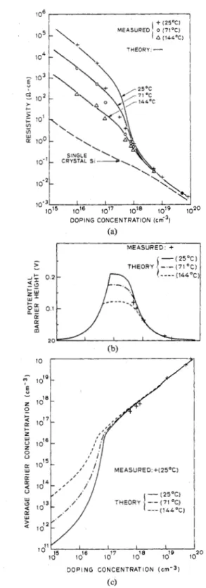
Fig. 9 is a plot of the linear least mean square approximation to the resistivity data normalized by the resistivity at 144°C versus l / k T . The slope of the approximation increases as the doping concentration is reduced [4]. Data for p versus N at 25", 71", and 144°C are plotted in Fig. 10. The slope of this curve becomes smaller at higher temperatures and moves to- ward the single-crystal curve.
111. THEORY
Polysilicon material is a three-dimensional substance with grains having a distribution of sizes and irregular shapes (Fig.
LU e t al.: MODELING A N D OPTIMIZATION OF RESISTORS 823 TABLE I
ROOM-TEMPERATURE CARRIER CONCENTRATIONS FOR SIX SAMPLES WITH DIFFERENT DOPING CONCENTRATIONS
(Unit: ern-')
Doping Con- Mcasurcd Calculatod Calculated
centration P N + P 5X1O1' 3.0X10'7 4 . 4 ~ 1 0 " 3.6 X loL7 8 X 10¹⁷ 5.1 X 10" 6.8X10" 6.1 X 10¹⁷ 1 x 10'8 7.1 X 10¹⁷ 8.4 X 10¹⁷ 7.8X10" 5 X lo'* 4.1 X 10'' 3.96X lo'* 3.9X 10" 1 x 10'0 9.9x10~8 1.0XlO'Q Q.99X 10" 5X10¹⁰ 6.0X 10" 5.0X10'0 5.0X10'0 M E A S U R E D : + (25'C) pB ( B A R R I E R ONLY) C R Y S T A L L I T E ) \ / - - - DOPING CONCENTRATION ( c m - 3 )
Fig. 8. Measured and theoretical hole mobility versus doping concen- tration of a polysilicon film with a grain size of 1220 A . The dashed
line indicates the calculation without including crystallite bulk mobility. T E M P E R A T U R E (O C ) 3 175150 125 100 75 MEASURED 0 L M S. FIT. - P ?
1
DOPING CONCENTRATION ( C m 3 ) (a)-
- ( 2 5 ' C ) 2 THEORY[-.-
( 7 1 ° C )-
U \t 1 ...:
Fig. 10. The model applied to different temperatures. (a) Measured andtheoretical resistivity versus doping concentration. (b) Corresponding potential barrier versus doping concentration. (c) Average carrier concentration versus doping concentration.
2). For simplicity, we assume that polysilicon is composed of identical cubic grains with a grain size L and that its transport properties are one-dimensional (Fig. 11). The applied voltage
Vu over all Ng grains between two resistor contacts is assumed
to be equally dropped across all grains (grain voltage is Vg = Fig. 9. Measured resistivity versus l / k T for samples with different
v~/N~).
The sinde-crystd silicon energy-band structure isdoping concentrations over a temperature range from 25" to 144°C.
The solid lines denote the linear least mean square approximations to applicable inside the CrYstaflites. For convenience, the intrin-
the data. sic Fermi level
4,
at the center of the grain is chosen t o be a1 / kT ( e V )
J,
0' 20
DOPING CONCENTRATION ( c m - 3 )
824 IEEE TRANSACTIONS ON ELECTRON DEVICES, VOL. ED-28, NO. 7 , JULY 1981
f
E:-qV(x) ELECTRONIC ENERGY ACCEPTOR LEVEL EA i i --I “2I-
“1-4
vz l- (C)Fig. 11. The modified polysilicon trapping model. (a) One-dimensional grain structure. (b) Energy-band diagram for p-type dopants. (c) Grain boundary and crystallite circuit. Only the partially depleted grain is shown. When completely depleted, there is no neutral region and the depleted region extends throughout the grain. When un- doped, there is no depleted region and the Fermi level is believed to lie near the middle of the band gap.
zero electronic energy; the energy is positive for upward and negative for downward direction. The grain boundary is of thickness 6 which is much smaller than
L
and containsQT
traps that are initially neutral and become charged at a certain monoenergetic level ET referred to Et, after trapping thecarriers.
A . Undoped (Nearly Intrinsic) Material
It is generally believed [12], [ 161, [ 191 that the chemical potential of polysilicon grain boundaries lies somewhere near the middle of the forbidden band gap. If no intentional dopant impurities are added into the deposited polysilicon film, the energy band is relatively uniform throughout the film; there- fore, other than grain-boundary effects, its behavior is similar to that of a uniform intrinsic single-crystal silicon. The resis- tivity of polysilicon p , therefore, is
where PGB is resistivity as a result of the grain boundary, and
p c is the single-crystal resistivity described by E261
where pa and p p are electron and hole mobilities, and the in-
trinsic carrier concentration ni is [26]
0.6
+d-UNDoPED MEASURED: THEORY:
-
++
0 I I I
1015 10’6 1ol8 1o19 lozo DOPING CONCENTRATION (cm-3)
Fig. 12. Experimental and theoretical activation energy versus doping concentration.
where the forbidden band gap of silicon Eg is [26]
7.02
x
10-~TZE, = 1.16
-
?“+I108 *
B. Doped Material
When polysilicon film is doped with one type of impurity, most dopants enter the crystallite lattice substitutionally and are assumed to be uniformly distributed throughout the film after subsequent thermal treatment. An impurity level is formed inside the crystallites, and impurity atoms are ionized to create majority mobile carriers [25]. The traps in the grain boundary charged by trapping mobile carriers deplete the re- gions in the crystallites, and potential barriers are thereby formed on both sides of the grain boundary (Fig. 1 l(b)). For simplicity, the depletion approximation, which assumes that mobile carriers are neglected and that impurity atoms are totally ionized in the depleted region, is used to calculate the energy-band diagram. Poisson’s equation becomes [4]
By integrating this equation twice and using the boundary con- ditions that V ( x ) is continuous and that dV/dx = 0 at x =
I,
the potential V ( x ) isq N ( x - 1)’
L
2E 2
V ( x ) = k
,
l < x < - .The potential barrier height V, is the difference between
V(L/2)
and V(0); that isqNW2 2E
v,
=+-where
+
denotes p-type dopants and - indicates the n-type,and W is the depletion-region width (L/2 - 1). The following
sections focus on p-type dopants; however, similar results can be derived for n-types.
1 ) Resistivity and Mobility: polysilicon resistivity is com-
posed of three serial components; one is the result of the po- tential barrier, and the second is the bulk resistivity of the
LU e t al.: MODELING AND OPTIMIZATION O F RESISTORS 825
crystallite. The third component represents the actual grain boundary and is negligible because of the very narrow bound- ary width [ 4 ] , [ 2 7 ] . Barrier conductivity is the consequence
of two components-thermionic emission and field emission across the barrier. Thermionic emission results from those carriers with an energy hi& enough to surmount the potential barrier; field emission stems from carriers with less energy than the barrier but capable of tunneling quantum mechanically through the barrier. For simplicity, only the barrier conduc- tivity from thermionic emission is derived. The study of field emission is described in [28]. The bulk resistivity of the
crystallite neutral region, resulting from lattice and impurity scatterings, is equal to the resistivity of single-crystal silicon
Thermionic-emission theory for metal-semiconductor Schot-
1291, ~301.
tky barriers demonstrates [26] that
* [exp T ) V / k ( 4 - 11 ( 8 )
where p ( 0 ) is the hole concentration in the equilibrium neutral
region [ 171 expressed [26] as p ( 0 ) = izi exp ( - E F / k T ) ( 9 )
where EF is the Fermi level with respect to Ei,. In polysilicon,
however, semiconductor material exists on both sides of the barrier. Rather than the metal-semiconductor junction used in some earlier models [ 4 ] , [ 1 7 ] , therefore, grain-boundary barriers are considered in these derivations as a symmetrical semiconductor-to-semiconductor junction [ 1 8 ] , [19]. The
grain voltage is dropped on both the barriers and crystallite bulk. The voltage across the barrier vba is assumed to be equally divided on each side of the junction, and the transport equation, therefore, becomes [ 181, [19]
k T ’I2
J =
2qp(O) (7exp )( - q V B / k T ) sinh2 nmh
where p ( 0 ) is the hole concentration at the center of the grain, as defined in (9). If vba
<<
2kT/q, thenOver this linear J- V range, barrier resistivity p~ (defined as the electric field divided by current density) is
Similarly, crystallite bulk resistivity is
vc
PC = J ( L - 2 W )
where V, is the voltage across the crystallite neutral region.
Total resistivity p , which includes pB and P C , is
p = % = p B p ) t p C ( l - T ) . 2 w
Substituting (12) into this equation results in a general expres-
sion for polysilicon resistivity.
Interpretation of carrier mobility in the nonhomogeneous polysilicon material is based on the assumption that an effec- tive mobility p e f f exists such that
1
p = - .
4PPeff
The average carrier concentration is defined as
and p ( x ) is the carrier concentration at point x determined by Maxwell-Boltzmann statistics [26] to be
The validity of p,ff was demonstrated by Set0 [4] for small grains and, in this work, for either small or large grain sizes. By combining (14) and ( 1 S), p e f f (including both barrier and bulk mobilities) can be obtained.
2) Calculations of W, VB, EF, p(O), and j7: This section de-
rives the quantities
w,
VB, EF, p(O), and j7 required for the cal-culation of p and p e f f . For small bias, EF is assumed to be
constant throughout the grain. The effective trapping state
density Q: (the ionized trap density in the grain boundary) is related to the number of metallurgical traps QT through the Fermi-Dirac statistics at temperature T as follows [ 4 ] , [3 1 ] :
QT
”
= 1+
2 exp (EF-
E T ) / k T ‘The degeneracy factor is 2 because the traps are assumed to be
identical and without interaction, and each can trap one hole of either spin. It is also assumed that ET is located at a con-
stant energy eT with respect to E j at the grain boundary, which is bent down by - qVB with respect to Ei, ; therefore,
Using the above two equations and the charge-neutrality con- dition, which equates the number of ionized dopants in the depletion region to the number of charged traps, results in
2NW = QT
1 t 2 exp [(EF - eT
+ qVB)/kT]’
Because Q$ and L are finite, a certain doping concentration N* exists for which the grains are totally depleted if N
<
N*(2 W = L ) ; otherwise, the grains are only partially depleted
826 IEEE TRANSACTIONS ON ELECTRON DEVICES, VOL. ED-28, NO. 7, JULY 1981
from that in the neutral region and is
EF = - k T l n
g).
Based on (7), (20), (21), and 2W = L , N * is iteratively deter- mined' as
N" =
-
2ni exp (- eT/kT) exp (q2N*L2/8ekT). (22)Completely Depleted Region, N
<
N*: When 2W
= L , and Lfrom (7) 4NL
Vi3
= 8 e .
From (20)) EF is determined t o be
and, based on (6)) (1 6), and (17)) the average carrier concen- tration is
which, when compared to Seto's derivation [4]
,
demonstrates that Set0 overestimated jT by a factor of exp (4 V'B/kT).Partially Depleted Region, N > N * : In midrange of the doping concentrations at medium and high temperatures for which silicon is nondegenerated [25]
,
the crystallite has both depletion and neutral regions. In the neutral region, the ionized impurity concentration NC at temperature T [26],
[31] iswhere EA is the acceptor impurity level within the forbidden band gap and, for boron, is [25]
E A =
-Eg
+
0.08 - 4.3 X 1 0 - 8 ~ 1 / 3 .2 (27)
Combining (9), (26), and the condition p(0) = N + yields N
1
+
2 exp [(EA - EF)/kT]ni exp (-EF/kT) =
and determines EF. By using (7), (9), (20), and p ( 0 ) =N+, W can be calculated by numerical iteration as follows:
W = QT
2 N [ 1 t 2(nj/N+) exp (-eT/kT) exp (q2NW2/2ekT)] (29) which is significantly different from the corresponding expres-
N * generally occurs in a medium-doped range where the difference can
'The partial ionization of dopants is not taken into account because be neglected so as to yield an analytical solution.
sion obtained by Seto [4] who implicitly stated that W = QT/2N. This difference is a result of the discrepancy between QT used by Set0 and Q; in this work. In a medium-doping concentration and for a large grain size (>400
A),
Q; becomes much smaller than Q T . If QT is used rather than Q;, N * is much larger than that calculated in (22)) and a discontinuity occurs near N" in the p versus N curve (Fig. 3). AfterW
is de- termined, the average carrier concentration becomesIn a very heavy doping concentration (such as >6.5 X IO1' ~ m - ~ ) of boron in silicon, the conduction and impurity bands overlap and the sample degenerates [25]
,
[26].
Because most impurity atoms are ionized and the depletion region becomes very narrow, the approximation j5 = p ( O ) m N is sufficient. The Fermi energy level can be calculated using the Fermi in- tegral instead of the Maxwell-Boltzmann approximation [26],
[321.
IV. COMPARISON BETWEEN THEORY AND EXPERIMENTS
To compare theory to experimental results, it is necessary to determine m l , e, ni, Eg, E A , L , QT, and e T . The values of
single-crystal silicon are assumed in the first five parameters [33]. Equations (3) and (4) were used t o calculate the tem- perature effect of n1 and Eg, respectively, and (27) derived the doping dependence of EA for boron; L was determined by TEM measurements and from I-V characteristics, and QT and
eT were obtained from the p versus l / k T curves.
A . Undoped Samples
Because the behavior of the p versus l / k T curves in Fig. 9 is nearly Arrhenius [34] from 25" to 144°C for undoped and all- doped samples, an activation energy of p versus l / k T can be defined as
Experimental Ea versus N is shown in Fig. 12. For undoped samples, it is assumed that y,, and yR are proportional to T-3/2 [30]. By neglecting the ~ G term in (l), B Ea X Eg/2.
In silicon, Eg 1.12 eV. For an undoped sample, therefore,
E, is predicted to be 0.56 eV which is in good agreement with
the experimental value of 0.55 eV. In addition, at T = 300"C,
ni = 1.45 X 10" ~ m - ~ , p,, = 1400 cm2/(V * s), and y, = 525
cm2/(V. s) [33], pc is calculated as 2.3 X lo5 S2 cm. The experimental resistivity of undoped polysilicon, which depends on deposition conditions and grain size, is approximately 2 to 8 X
io5
~ 2 .
cm.B. Doped Samples
The distribution of grain size by dark-field TEM was studied in Section 11-A [14], and L was derived in (10) as follows. Both the small- and large-signal I-V characteristics were deter-
LU e t al.: MODELING AND OPTIMIZATION O F RESISTORS 827
mined for rectangular resistors with doping concentrations of TABLE I1
1 X 10l8 cm-3 and lengths of 80 and 120 pm (Fig. 5). Be-
cause measured resistivity is much higher than that of single- crystal silicon, grain voltage is assumed to drop across the bar- riers (Vba
*
Vg = V,/Ng). Equation (10) can now be rewrittenas
TRAPPING STATE ENERGY AND DENSITY OF SAMPLES WITH
DIFFERENT DOPING CONCENTRATIONS
N E o er Q r
(cmVa)
(ev)
( WI = JA = 2 I, sinh
(
-
2:g: T )
where A is the cross-section area of the resistor, and I, is the
pre-sinh factor in (10) multiplied by A . If Va/Ng
<<
2 k T / q ,resistance R = V/I at small bias becomes R *Ngk T/q I , . By
eliminating I, from the above
I =
(
7
sinh(-1
)
2NgkT
As a result, Ng can be determined by measuring R at T and us- ing (33) to fit the large-signal I-Vdata, and so L is obtained from the length between the two resistor contacts divided by Ng. The number of grains is in good proportion to resistor length, which supports our assumption that the transport in polysili- con is nearly one dimensional through cubic grains. The hyper- bolic-sine I-Vcharacteristic observed in ring-and-dot structures, however, indicates that the number of grains is not directly proportional to the length between the two contact rings be- cause the conduction in these devices under large bias may be two-dimensional in contrast to one-dimensional in rectangular resistors. It was found that L
=
1220A
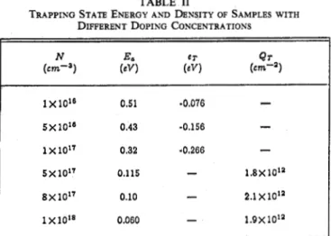
which is smaller than the average grain size but close to most values observed by TEM (Fig. 4); a small deviation occurs in different doping concentrations.The parameters QT and eT are determined as follows. For N G N " , inserting (3), (9), (24), and 2 W = L into (12) results
in 1 x 10'8 0.51 -0.076
-
5 X 10:' 0.43 -0.156-
1 x 10¹⁷ 0.32 -0.266-
5 X l o l l 0.115-
1.8X10¹² 8 X l O " 0.10-
2.1 x 10'1 (33) 1 x 10'8 0.060-
1.9x 10'2 and, from (3 1 ) E a m E g + e T + k T 2and 1 X 10l8 cm-3 produces V, from (35) and then W from
(7). Based on QT
=
Q$
= 2NW, Q T can be determined at eachdoping level, respectively (Table II), and an average value of
1.9 X lo1' cm-? was selected. The first-order estimation of
eT was obtained from the Ea of samples where N = 1 X
5 X and 1 X 1017 cm-3 from (34) (Table 11), and an av- erage value of - 0.17 eV was chosen. (Calculated N" at room
temperature is approximately 7.3 X 10l6 ~ m - ~ . AlthoughN=
1 X lo1' > N * , its Ea is not far from the completely depleted
conditions and still is applied for estimating eT.) Because L
and QT have been determined, the value of
eT
was adjusted toproduce the best fit of the p versus N, p versus N, and p versus
l / k T curves; this is equivalent to Seto's method where jj was
used in the completely depleted samples to obtain that value. After the parameters are determined, data for p versus N
and p versus N can be more accurately modeled by introducing
f into (12) as follows:
For N
>
N * , the following conditions are considered:1 ) If N is near N * ,
QG
<<
QT,
V, becomes a complicatedfunction of temperature as does p , and E, cannot be expressed
in a useful analytical form.
2 ) When N increases,
Q$
=
QT and p ( 0 ) becomes a weakfunction of temperature. From ( 1 2 )
p a T'12 exp (qV,/kT) (3 5 a)
and, from (3 1 )
E, m qVB - 3kT. (35b)
3) If the sample is more heavily doped, the resistivity con- tains barrier and bulk components and, therefore, its tempera- ture behavior is affected by both components.
The experimental data demonstrate that condition 2 ) ranges
from 5 X 10l7 to 1 X l o n 8 cms3 and is suitable for determin- ing QT. The activation energy for N = 5 X lo", 8 X lo",
Fig. 13 is a flow chart of the computer program for this model- ing, and the parameter values chosen to fit the data are listed in Table 111. An artificial factor n used by Set0 [4] and in [ 7 ]
is not required in (36) to model the p versus N curve above
room temperature because, based on thermionic theory [ 1 7 ] , [ 2 6 ] , p ( 0 ) is used instead of
p .
By comparing (9) to ( 2 5 ) or(30), it can be seen that, in the near N " region, p ( 0 ) is par-
ticularly larger than
p
which causes p to be much smaller than that calculated by use of jT which is equivalent to the function of the n factor. Calculation ofp ,
however, is still helpful in interpreting effective mobility and in observing how traps reduce the number of mobile carriers. The reduction of car- riers in lightly and medium-doped ranges is mostly the result of traps but, in the highly doped regions, the partial ionization of dopants caused by the existence of an impurity level be- comes more important. For example, at a doping level of1 X 10l8 ~ m - ~ , approximately 16 percent of the dopants
are unionized, but less than 10 percent of the carriers are trapped at room temperature. This effect becomes signifi- cant at lower temperatures and, in addition to the segregation effect [ 171, it contributes to the smaller carrier concentration
828 IEEE TRANSACTIONS ON ELECTRON DEVICES, VOL. ED-28, NO. 7 , JULY 1981
ril
INPUT Nrn
N Q Ne?-N > MAXIMUM N 7
1
Fig. 13. Flow chart of the computer program for the model. Numbers within the parentheses refer to the equations in text.
TABLE I11
PARAMETER VALUES TO FIT DATA OF POLYSILICON FILMS WITH DIFFERENT GRAIN SIZES
L
Data Source Q T L
I
From ( 4 (cm-l) ( 4
Ref'. 4 -0.18 3.34X10" 230 0.12 This work -0.17 1 . 9 ~ 1 0 ~ ~ 1220 0.060
than doping concentration in highly doped samples. The .theoretical p versus N curve in Fig. 8 demonstrates the
importance of the crystallite bulk mobility. In the range of
N < N " in Fig. 12, the calculated almost constant E, is not
in accord with the experimental E, which increases up to
0.55 eV as the doping concentration reduces to the intrinsic conditions.' This is because the trapping states are assumed to have a 6-shaped distribution; however, in the real substance, these states must have some type of distribution over an energy range. In addition, the simplified assumptions that all grains are of the same size and become completely depleted at the same N * and that the abrupt depletion approximation is used
to derive the energy band cause the calculated values to de- viate from the data, especially around N " .
The effect of grain size on the electrical properties of poly- silicon is shown in Table 111. The trapping state energy remains approximately at the same level as the grain size varies, and
2Because of the mistake in Seto's derivation [4], his theoretical curve in Fig. 9 shows an erroneous prediction in the range of N < N * . The
sharp change of E, versus N near N * in [ 171 is eliminated by exact
computer calculations.
L n 2 3 0 A ( R E F E R E N C E
10-2-
Fig. 14. Influence of e T , L , and QT on the slope of room-temperature resistivity versus doping concentration. The curve for Seto's data [4] is used as a reference, and its parameter values are listed in Table 111.
Curve (1) shows the jeTl change from 0.18 to 0.17 eV; curve (2) re- sults from increasing L from 230 to 1220 A , and curve (3) is obtained by reducing QT from 3.34 X 1OI2 to 1.9 X l 0 l 2 cm-2. In these plots, f = 0.12 and single-crystal resistivity is included. Curve (4) is based on the parameter values for our data in Table 111, a n d f = 0.06.
QT reduces with increasing grain size. This can be expected as a result of a drop in the degree of disorder in the material as it changes from polycrystalline toward single crystal. The sensitivity of the p versus N curve in Fig. 1 also decreases as
grain size increases; it is instructive to use this model to deter- mine the influence of the material parameters on the slope. In Fig. 14, the solid line plots the theoretical results for Seto's data [4] for reference. It can be seen that the slope of curve (1) becomes worse as leT[ changes from 0.18 to 0.17 eV. As
L increases from 220 to 1220
A
in curve (2), p decreases inthe completely depleted region and the slope falls; in curve (3), p drops mainly in the partially depleted region as QT is reduced from 3.34 X 10l2 to 1.9 X 10l2 crn-'. If
QT
and L change at the same time as does curve (4) and the crystallite bulk effect is added, the slope of p versus N falls sharply.The artificial factor f, which increases p by (I/f) times with respect to the calculated values, requires further inves- tigation; one of the first steps is to study its temperature behavior. Assuming that
QT,
e T , and L are temperature in-dependent and based on the temperature effect of yli and ER in (3) and (4) and the slight variations in pc [29], [30], the theoretical results of the p versus N curves in Fig. 10 demon- strate the validity of the model over a wide temperature range. It is also found that f is almost temperature independent. Because the calculated and measured and V, are in good
agreement, the increases in p as a result of f cannot be attrib- uted to segregation or modeling inaccuracy. In addition, the doping concentration is too low to cause localization or clustering of dopants. Two explanations are possible. One is that the effective Richardson constant (effective hole mass) is much smaller than in the single crystal, which may occur in such disordered structures as polysilicon. The second is that some transmission probability exists when carriers pass
LU et al.: MODELING AND OPTIMIZATION O F RESISTORS
RESISTIVITY ( i l - c m ]
Fig. 15. Measured activation energy versus resistivity of polysilicon
films with different grain sizes at 25" and 144°C.
through the complicated grain boundary by either scattering or recombination.
V. DESIGN CRITERIA
Based on the experimental success of the modified trapping model, the following criteria to optimize resistivity control, linearity, and temperature sensitivity in the design of poly- silicon resistors [ 2 ] , [ 2 3 ] are discussed in this section.
For good resistivity control, grain size must be increased. For high linearity, Vg must be small. Polysilicon resistors are
nonlinear as V,
=
2kT/q. Although the nonlinearity of an80-pm resistor becomes appreciable above 30 V (Fig. 5 ) , the
same nonlinearity appears even at 2 V in a 5-pm resistor by
proper scaling [ 2 3 ] . Because
&
= V,/N,, a lower applied biasacross the resistor, a longer resistor, or a smaller grain size can reduce
Vg
to enhance linearity, The voltage coefficient ratio of resistance (VCR) is defined and used for quantitative char- acterization of linearity; that is(37)
For less temperature dependence, resistivity must be lowered. From the nearly Arrhenius behavior of p versus l / k T , the
curve of E, versus p should be a straight line when p~
>>
pcand the slope is WkT. Fig. 15 plots the experimental results
obtained from six runs and data from Set0 [4] at 25' and
144OC. This demonstrates that, independent of the poly- silicon-resistor fabrication process, a specific p has a specific
E a ; for higher p , E, is larger. The matching of polysilicon
resistors with respect to the operating temperature is com- parable to diffused resistors over the above temperature range. In applications where resistivity ratio matching [ 3 5 ]
or the absolute value [ 3 ] is critical, E, can be suitably selected based on the specified resistivity variations over the operating temperature range and Figs. 9 and 15 to reduce circuit-temper- ature sensitivity and, therefore, to optimally determine p .
For low-temperature sensitivity,
Vg
must be large. If the resistors are operated over a nonlinear range, V, becomes afactor in addition to E,. The dc temperature-coefficient ratio TCRd, is defined as TCRd, = ( l / R ) ( d R / d T ) which shows that TCR depends on E, and V,. In a partially depleted region
where p ( 0 ) is independent of T and V,, V,
TCRd, = --
[-
T kT 2 2NgkT
(
2 i g t T ) ]@-B + - - - qVa coth ~
Because of a minus sign before the
V ,
term, TCR can be re- duced by increasingVg
(raising V, or reducing Ng) [2].
If the resistor is operated at higher temperatures, the sensi- tivity of p versus N will be improved (Fig. lo) and TCR can also be reduced in (37).
For good isolation, reduced parasitic effects, and less sub- strate bias dependence, the oxide underneath the resistor must be thick.
There are some tradeoffs, however, among these criteria. Large grain size can result in better resistivity control and a lower TCR but less linearity; high resistivity can save die area but produces larger temperature sensitivity. These criteria derived quantitatively from the model become important, therefore, in the optimization of resistor design.
VI. CONCLUSIONS
A modified trapping model for polysilicon with either small or large grain sizes under different applied voltages has been developed and has been successfully applied to p-type poly- silicon. It is equally applicable to 0.67-pm thick n-type polysilicon films [7] where an electron trapping level exists
at ~ 0 . 2 eV above
Ei
at the grain boundary. In addition, be- cause the postannealing electrical properties of low-pressure CVD (LPCVD) and atmospheric-pressure CVD polysilicon fdms are similar [ 8 ] and the modeling parameters are deter- mined from experiments, the applicability of the model to thin LPCVD polysilicon films is feasible. It has also been demonstrated theoretically and experimentally that the long- existing problem of resistivity control can be solved by in- creasing the grain size and stabilizing the dopant distribution. In addition, criteria concerning temperature sensitivity and linearity have been established to optimize device design.In this work, a high deposition temperature or thick poly- silicon film was used to increase grain size. For LPCVD films or in some processes that cannot withstand high temperatures, laser annealing [ 2 1 ] , [ 3 6 ] , [ 3 7 ] , the neutron-transmutation method for doping polysilicon to reduce QT and to lower the anneal temperature so as to avoid segregation [ 121, and
hydrogen-plasma annealing to change QT [ 3 8 ] become attrac- tive. For more critical control of resistivity, nitride instead of oxide can be used as the passivation layer to avoid boron leaching.
The model has the advantage of being analytical. It is some- what inadequate, however, for the following reasons.
Although the &-function approximation of trapping-state density obtains better results than does continuous distribu- tion [ 1 2 ] , [ 1 7 ] , the assumption of a 6-shaped approximation limits the theoretical prediction that E, versus N is constant
when N
<
N " , which is not in agreement with the experimentalresults. It is likely that the trapping states are distributed over a specific energy range. In our estimation, a Gaussian distri- bution with a small standard deviation is the most probable
829
![Fig. 3. Theoretical room-temperature resistivity versus doping concen- tration of a grain size of 1220 A based on [4] and [ 171](https://thumb-ap.123doks.com/thumbv2/9libinfo/7678157.142001/3.899.70.443.58.321/theoretical-temperature-resistivity-versus-doping-concen-tration-grain.webp)