國
立
交
通
大
學
電子工程學系 電子研究所碩士班
碩 士 論 文
在
PlayStation 3 上的即時多媒體處理
Real-time Multimedia Processing on PlayStation 3
研究生: 陳慶至
指導教授: 劉志尉 博士
在
PlayStation 3 上的即時多媒體處理
Real-time Multimedia Processing on PlayStation 3
研 究 生:陳慶至
Student: Ching-Chih Chen指導教授:劉志尉 博士
Advisor: Dr. Chih-Wei Liu國 立 交 通 大 學
電子工程學系 電子研究所碩士班
碩士論文
A Thesis
Submitted to Department of Electronics Engineering & Institute of Electronics College of Electrical and Computer Engineering
National Chiao Tung University in Partial Fulfillment of the Requirements
for the Degree of Master in
Electronics Engineering
October 2007
Hsinchu, Taiwan, Republic of China
在 PlayStation 3 上的即時多媒體處理
研究生:陳慶至
指導教授:劉志尉 博士
國立交通大學
電子工程學系 電子研究所
摘要
現 今 的 多 媒 體 發 展 非 常 迅 速 , 為 了 提 升 資 料 速 率(data rate) 和 壓 縮 比 率 (compression ratio),使得演算法的複雜度不斷增加。所以通常會使用可程式化處理器 而非特定功能積體電路(ASIC),以因應各種新穎的多媒體標準。在處理器為主的平台 上,只需要作軟體的更新,就可以讓新的多媒體應用能夠順利運行,延長產品在市場 的壽命。在多媒體應用中,除了傳統處理器所利用到的指令層級的平行度(ILP)和資料 層級的平行度(DLP)之外,多執行緒(multi-thread)或多核心(multi-core)架構進一步利用 執行緒(thread)層級的平行度(TLP)。多核心處理器能提供很高的運算能力去處理複雜 的應用,但是多核心處理器的程式撰寫非常困難。多核心程式撰寫有兩個最主要的問 題是,由工作分派所產生的同步花費和工作之間資料傳遞所產生的溝通花費。本論文 中採用以幅為基礎(frame-based)的資料切割方式,去消除工作之間的資料依靠關係 (data dependency),減少同步的花費。溝通的問題則是利用資料流動最佳化來解決。在 一個著名的多核心架構—PlayStation 3 上,可以使用這些技巧對一個 1080p 多媒體影 片解碼器作最佳化。由實驗結果可知,這些最佳化的技巧能使解碼器加速20 倍,最後 超過即時(real-time)的限制以 60Hz 的頻率解碼出 1080p 的影片。Real-time Multimedia Processing on PlayStation 3
Student: Ching-Chih Chen Advisor: Dr. Chih-Wei LiuDepartment of Electronics Engineering Institute of Electronics
National Chiao Tung University
ABSTRACT
Today’s multimedia applications evolve very fast. In order to improve the data rate and compression ratio, the complexity of algorithm is enhanced. Instead of ASIC, programmable processors are usually used to deal with the variety of new multimedia standards. Processor-based architectures can use software patches to keep up with new multimedia applications, thus extend products’ time-in-market. However, conventional processor architectures are unable to provide sufficient computing power for real-time constraints. Beyond instruction-level-parallelism (ILP) and data-level-parallelism (DLP) used in conventional processors, multithreaded/multi-core architecture further acquire thread-level-parallelism (TLP) to exploit parallelism in multimedia applications. Multi-core processor can provide high computing power to support complex applications, but multi-core programming is much more difficult. There are two main issues in multi-core programming, synchronization overhead introduced by task parathion and communication overhead arising from data communications between tasks. In this thesis, we adopt frame-based data partition to eliminate the data dependency between tasks, thus minimize synchronization overhead. Communication problem is solved using dataflow optimization. Using these techniques, a multimedia video decoder processing 1080p frames is then optimized on a famous multi-core architecture – PlayStation3. The experimental results show that the optimization techniques make the decoder run 20-time faster, which finally exceed real-time constraint to decode 1080p frame at 60 Hz.
誌 謝
研究生涯轉眼即逝,兩年來受到許多人幫助及鼓勵,才能如此順利完成碩士學業,在 此致上最深的感激。 感謝劉志尉老師。老師的豐富學養及學者風範,使我在專業知識及研究態度上,更臻 成熟,感謝老師兩年來的指導。同時,感謝口試委員:張錫嘉教授及闕河鳴教授。謝 謝你們在百忙之中,撥冗參與論文口試,並對我的研究給予寶貴的意見,讓此篇論文 更加完備充實。 感謝林泰吉學長。泰吉學長不厭其煩地對我的研究工作步步導引,有他的指導協助, 才能有今日的成果。學長亦師亦友,研究所其間與學長相處的點點滴滴,都是求學階 段最美好的回憶。 感謝實驗室學長學弟們。感謝陳信凱學長、歐士豪學長、林禮圳學長及郭羽庭學長, 感謝學長們在研究生生涯中的各項協助及鼓勵。感謝洪正堉、顏于凱、呂進德、林彥 呈、張巍瀚及李岳泰,謝謝學弟們在研究工作上的一切幫忙。 感謝一起打拼的好伙伴:王炳勛、卓毅、鄧翔升、劉士賢及卓志宏。這兩年,我們一 同經歷了挑燈夜戰的努力,也共同分享研究成果的喜悅。 最後,感謝我最親愛的家人。爸、媽、哥,感謝你們一路上的支持及鼓勵,沒有你們 就沒有今日的我,我愛你們。 謹將此篇論文獻給所有曾支持我、協助我的人,衷心的感謝並祝福你們。 慶至 謹誌於 新竹 2007 秋Contents
ABSTRACT (CHINESE)... i
ABSTRACT (ENGLISH) ...iii
ACKNOWLEDGEMENT ... v CONTENTS ... vii LIST OF TABLES ... ix LIST OF FIGURES... xi 1 Introduction...1 1.1 Multimedia Processing ...1 1.2 Multi-core Processors...2 1.3 Thesis Organization...4 2 Background ...7
2.1 Cell Broadband Engine...7
2.2 Programming on PPE and SPEs ...19
3 Frame-based Data Partitioning on CBE ...24
3.1 Port the Multimedia Applications to CBE...25
3.2 Functional Partitioning and Data Partitioning for Multi-Core Processor...28
3.3 Comparison between Data and Functional Partitioning...28
3.4 The Partitioning and Management of Multimedia Decoding on CBE ...30
3.5 Dataflow Planning for Multimedia Decoding on CBE ...36
3.6 DMA and Buffer Allocation on CBE ...38
4 Experimental Results...45
4.1 The Transfer Size per DMA Command...50
4.2 The Size of I/O Buffer ...52
4.3 The Double Buffering...55
4.4 The Utilization of Different Number of SPEs ...58
5 Summary and Future Work ...62
List of Tables
Table 2-1 Differences between PPE and SPE...9
Table 2-2 Three primary mechanisms of interprocessor communication ...17
Table 2-3 The reason why we have SPE initiate DMA commands...18
Table 2-4 The mailbox channels and their associated MMIO registers ...19
Table 3-1 Data partitioning vs. functional partitioning ...30
List of Figures
Figure 1-1 Multi-chip module vs. multi-core processor...3
Figure 2-1 The block diagram of CBE processor...8
Figure 2-2 Brief block diagrams of PPE and SPE...9
Figure 2-3 The PowerPC Processor Element (PPE)...10
Figure 2-4 The synergistic processor elements (SPE)...12
Figure 2-5 The functional units in SPU...13
Figure 2-6 The element interconnect bus (EIB) ...15
Figure 2-7 Maximum bandwidth of Cell processor ...16
Figure 2-8 The API of DMA ...20
Figure 2-9 The API of mailbox...20
Figure 2-10 The cooperation of PPE and SPEs...21
Figure 3-1 Port the Multimedia Applications to CBE ...25
Figure 3-2 Functional partitioning and data partitioning ...27
Figure 3-3 The situation of LS in the multimedia decoding...31
Figure 3-4(a) Data dependency in JPEG ...33
Figure 3-4(b) Spatial data dependency in H.264...33
Figure 3-5 Data communication between LS and shared memory ...35
Figure 3-6 Dataflow planning for multimedia decoding on Cell ...37
Figure 3-7 The input buffer is a ring structure ...39
Figure 3-8 The single output buffer...40
Figure 3-9(a) Single buffering...41
Figure 3-9(b) Double buffering ...41
Figure 3-10(a) The computation time of SPU is much less than the DMA time of MFC ...42
Figure 3-10(b) The computation time of SPU is much more than the DMA time of MFC ...42
Figure 3-11 The I/O double buffer ...43
Figure 4-1 The code structure of experimental program...47
Figure 4-2 The double frame buffer ...48
Figure 4-3 The performance with combinations of optimization techniques...49
Figure 4-4 The transfer size per DMA command...50
Figure 4-5 The size of output buffer...53
Figure 4-6 The double buffering for different transfer size per DMA command...56
Figure 4-7 The double buffering for different output buffer size ...57
Figure 4-9 The utilization of different number of SPEs (original version) ...59 Figure 4-10 The utilization of different number of SPEs (optimized version)...60
1 Introduction
The software-only solutions for media-rich consumer-electronics devices get more and more popular. This kind of solution decrease the development and manufacturing cost as long as the performance meets the real-time requirements of multimedia processing. The problem is how to reach the required level of performance on an advanced processor-based platform provided by the processor designers.
1.1 Multimedia Processing
The data rate and compression ratio of multimedia processing are improved as the complexity of algorithm grows. In multimedia decoding applications, the high-definition (HD) resolution is a basic requirement in many markets, such as DTV, multimedia games, and multimedia playing on monitors. The even higher performance pursued by consumers make
engineers design more powerful devices while keeping the price low.
There are 3 major parallelisms in multimedia applications: instruction-level parallelism (ILP), task-level parallelism (TLP), and data-level parallelism (DLP). These parallelisms could be exploited by 3 techniques respectively: the multi-issue, the single instruction multiple data (SIMD), and the multi-thread or multi-core architecture.
The high-end consumer electronics need to run versatile multimedia applications. For examples, audio standards are AAC, MP3, Dolby Digital (AC3), etc. And multimedia standards are M-JPEG, MPEG-1, 2, and 4, H.263, H.264, etc. Thus the implementation of multimedia coding by software is a cost-effective solution. Processor-based architectures can use software patches to keep up with new multimedia applications. However, conventional single-core processor architectures are unable to provide sufficient computing power for advanced real-time multimedia processing. Thus the parallelisms in multimedia applications should be exploited by processor-based system with high performance to meet the real-time specifications.
1.2 Multi-core Processors
In the recent years, the processor industry has reached a new market of consumer electronics and personal computers. In order to further improve the already high performance of processor, the concept of multi-core on a chip comes out. With the improvement of semiconductor processes, it’s possible to put many processing cores onto a single processor chip [1]. This kind of processor is called as multi-core processor or chip multiprocessor. It may be simply named as multiprocessor.
There are some reasons for this trend. First, the processor needs more effective performance per Hz, i.e., the power would become the bottleneck of processor. The utilization
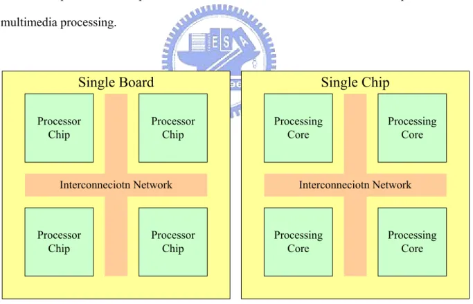
of more processors on a system was a common solution in the past. The multi-chip module (MCM) belongs to this category. But with the help of semiconductor technology, the integration of many circuits into a single chip is feasible. Figure 1-1 depicts this trend. The processor designers could now improve the processor performance just by making a single processor chip more compact, i.e., put more processing cores together on a chip. Furthermore, many standards for audio and multimedia have the same functionality but are almost not used simultaneously. These are the reasons why the general-purpose processors but not the application-specific integrated circuits (ASIC) are the solutions of multimedia processing for personal devices. Because the generic processors are broadly applicable, the cost of development and production could be decreased. This is the motivation to design the multi-core processor for performance in order to meet the real-time requirements of multimedia processing.
Processor Chip Processor Chip Processor Chip Processor Chip Interconneciotn Network
Single Board
Processing Core Processing Core Processing Core Processing Core Interconneciotn NetworkSingle Chip
Figure 1-1 Multi-chip module vs. multi-core processor
Cell, also known as the Cell Broadband Engine Architecture (CBEA), is a famous multi-core processor created by Sony, Toshiba, and IBM (called STI). It’s a design project to
provide power-efficient and cost-effective high-performance processing for a wide range of applications. It has been used in servers known as Cell blade, game consoles known as PlayStation 3. Cell is the multi-core system where this thesis holds experiment.
With the advent of multi-core processors, the programmers and consumers may simply think that the performance would increase linearly with the number of cores on a single chip. However, it’s usually not the case as we expected. The potential problems are the level of parallelism and the communication between each core. It’s a hard job to find a balanced workload for each core. The communication in a multi-core system may become the bottleneck when the communication time is too much or frequency is too high. Thus the key point to improve the performance of a multi-core system to an acceptable and reasonable level is task partitioning and communication between each core.
1.3 Thesis Organization
This work proposes a data partitioning scenario for media processing on Cell. The goal is to improve the performance with the number of cores utilized on Cell as linearly as possible. Namely, the number of frames per second of the decoding process is the performance index while the number of cores utilized is increased. The rest of this thesis is organized as follows.
Chapter 2 reviews the experimental platform: Cell Broadband Engine (CBE). A brief description of the architecture of Cell processor is the beginning. Two processing units called as the Power Processor Element (PPE) and the Synergistic Processor Element (SPE), the direct memory access (DMA), and the element interconnect bus (EIB) would be in the description. Then the communication mechanisms and associate application programming interface (API) are presented. A flow of porting the multimedia processing onto CBE is shown after the introduction is made.
Chapter 3 proposes a frame-based data partitioning technique for multimedia processing. A simple discussion of functional partitioning and data partitioning is presented. This chapter provides the data management and dataflow planning for multimedia stream decoding on CBE. The proposed technique tries to reduce the number of communication between each core, i.e., it tries to avoid the data dependencies between each partition of data. The optimization of data transfer via DMA is a key point to mitigate the communication burden on EIB of CBE. This is considered in Chapter 3 and discussed in Chapter 4.
Chapter 4 experiments the size of DMA and the allocation of buffer in local store. After the data management and dataflow planning implement as in Chapter 3, the details of data transfer between the local store and shared memory need to be considered. The suitable transfer size per DMA command and the I/O buffer allocation are found here. By the co-working of dataflow planning and the optimization of DMA, the performance boots to an expected level.
Chapter 5 summarizes this thesis and provides the future work.
2 Background
This chapter provides background information on topics related to this thesis. Chapter 2.1 gives an overview of the hardware platform, Cell Broadband Engine (CBE) [7][13][15]. Chapter 2.2 gives a flow of porting the multimedia decoding application onto CBE.
2.1 Cell Broadband Engine
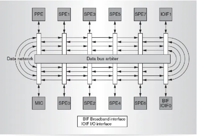
The Cell Broadband Engine is the first incarnation of a new family of microprocessors conforming to the Cell Broadband Engine Architecture (CBEA, or, informally, "Cell"). The CBEA is a new architecture that extends the 64-bit PowerPC Architecture. The CBEA and the Cell Broadband Engine are the result of collaboration between Sony, Toshiba, and IBM, known as STI, formally started in early 2001 [2][3].
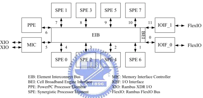
Figure 2-1 shows the block diagram of CBE processor hardware. The CBE processor is a multi-core processor with 9 processor elements and a shared coherent memory on-a-chip. The functionality of 9 processors can be specialized into 2 categories: the Power Processor Element (PPE) and the Synergistic Processor Element (SPE). There are 1 PPE and 8 SPEs in the CBE processor. In order to improve the productivity of PlayStation 3, only 6 SPEs are available for the programmers.
SPE 1 SPE 3 SPE 5 SPE 7
SPE 0 SPE 2 SPE 4 SPE 6
PPE MIC IOIF_1 IOIF_0 EIB BEI 0 11 10 9 8 7 6 5 4 3 2 1 FlexIO FlexIO XIO XIO
EIB: Element Interconnect Bus BEI: Cell Broadband Engine Interface PPE: PowerPC Processor Element SPE: Synergistic Processor Element
MIC: Memory Interface Controller IOIF: I/O Interface
XIO: Rambus XDR I/O FlexIO: Rambus FlexIO Bus
Figure 2-1 The block dia ram of CBE processor
The PPE complies with the 64-bit PowerPC Architecture. PPE could run 32-bit and 64-b
g
it operating systems and applications. On the other hand, the SPE is optimized for running compute-intensive applications. The PPE and the SPEs could work in a collaborative scenario. The PPE runs the operating system and the top-level thread control for applications. The SPEs provide the computing power to boot the performance of applications. Brief block diagrams of PPE and SPE are shown in Figure 2-2 [4].
Figure 2-2 Brief block diagrams of PPE and SPE
The Cell processor could be viewed as a 9-way multiprocessor for the application programmer. The PPE is suitable for control-intensive tasks and task switching. The SPEs are suitable for compute-intensive tasks but not task switching. The more significant difference between the SPE and PPE lies in how they access memory. The PPE can access main storage at all 264 memory addresses, also called effective addresses (EA), with the help of caches. The SPEs, in contrast, access main storage with the help of direct memory access (DMA) commands directed explicitly by programmers. Each SPE has its own local store (LS) which contains 256 KB. The LS is a scratchpad memory of each SPE and could be access by PPE or other SPE via DMA. Table 2-1 summarizes some differences between PPE and SPE.
Table 2-1 Differences between PPE and SPE
Feature PPE SPE
Addressability 2
64bytes
256-KB LS
Load Latency
variable (cache) 6
cycles
[20]
128-bit SIMD Registers
32
128
Doubleword SIMD
no
yes
PowerPC Processing Elements
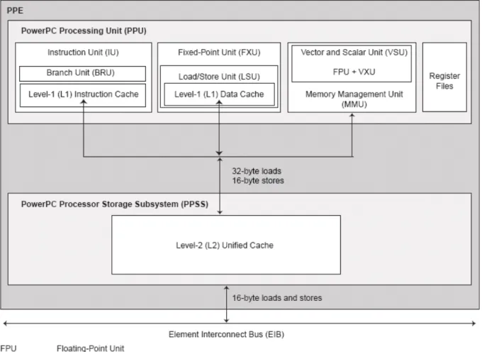
The PowerPC Processor Element (PPE) is a general-purpose, dual-threaded, 64-bit RISC processor with the vector/SIMD multimedia extensions. The PPE is responsible for overall control of a CBE system and the operating systems. The PPE consists of two main units as shown in Figure 2-3 [4]. The PowerPC processor unit (PPU) is the computation unit, and the PowerPC processor storage subsystem (PPSS) is for the purpose of storage.
Figure 2-3 The PowerPC Processor Element (PPE).
The PPU could further divided into the following units. • Instruction Unit (IU)
KB. The cache-line size is 128 bytes. The IU performs the instruction-fetch, decode, dispatch, issue, and completion portions of execution.
• Branch Unit (BRU)
The BRU performs the branch functionality. • Fixed-Point Unit (FXU)
The FXU performs fixed-point operations, including add, multiply, divide, compare, shift, rotate, and logical instructions.
• Load and Store Unit (LSU)
The LSU contains a 4-way set-associative and write-through L1 data cache with 32 KB. The cache-line size is 128 bytes. The LSU performs all data accesses, including load and store instructions.
• Vector/Scalar Unit (VSU)
The VSU contains a floating-point unit (FPU) and a 128-bit vector/SIMD multimedia extension unit (VXU), which together execute floating-point and vector/SIMD multimedia extension instructions.
• Memory Management Unit (MMU)
The MMU contains a 64-entry segment look-aside buffer (SLB) and 1024-entry, unified, parity protected translation look-aside buffer (TLB). The MMU manages address translation for all memory accesses.
The PPSS contains a unified, 512-KB, 8-way set-associative, write-back L2 cache with error-correction code (ECC). The cache-line size for the L2 is 128 bytes as the same as L1 cache-line size. The PPSS handles all memory accesses by the PPU and memory-coherence (snooping) operations from the element interconnect bus (EIB). The PPSS performs data-prefetch for the PPU and bus arbitration and pacing onto the EIB. There are MMU, L1 instruction cache, and L1 data cache of PPU getting data from PPSS by a shared 32-byte load port. There are MMU and L1 data cache of PPU putting data to PPSS by a shared 16-byte
store port. The interface between the PPSS and EIB supports 16-byte load and 16-byte store buses.
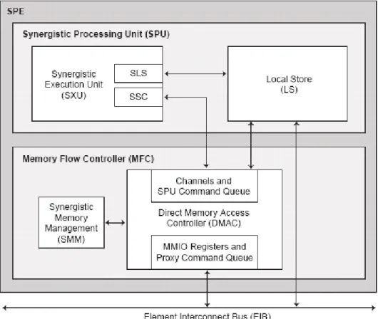
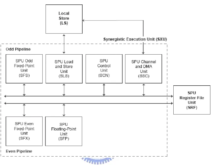
Synergistic Processor Elements
Figure 2-4 The synergistic processor elements (SPE)
Each SPE is a 128-bit RISC processor for data-rich, compute-intensive applications. It consists of two main units, the synergistic processor unit (SPU) and the memory flow controller (MFC), as shown in Figure 2-4 [4]. The data interface consists of a 128-bit read bus and a 128-bit write bus. The MFC can send up to 16 outstanding MFC commands. It supports atomic requests and snoop requests (read and write) of the SPU’s LS memory and the MFC’s
MMIO registers.
Figure 2-5 The functional units in SPU
Figure 2-5 shows the functional units in SPU. The SPU issues two instructions to its two execution pipelines respectively. The pipelines are referred to as even (pipeline 0) and odd (pipeline 1). The units in SPU could be pointed out as follows.
• SPU Odd Fixed-Point Unit (SFS)
The SFS executes byte shift, rotate mask, and shuffle operations on quadwords. • SPU Load and Store Unit (SLS)
The SLS executes load and store instructions and hint for branch instructions. It also handles DMA requests to the LS.
The SCN fetches and issues instructions to the two pipelines. It performs control functions such as branch instructions, arbitration of access to the LS and register file, etc. • SPU Channel and DMA Unit (SSC)
The SSC manages communication, data transfer, and control into and out of the SPU. • SPU Even Fixed-Point Unit (SFX)
The SFX executes arithmetic instructions, logical instructions, word SIMD shifts and rotations, floating-point comparisons, and floating-point reciprocal and reciprocal square-root estimations.
•SPU Floating-Point Unit (SFP)
The SFP executes single-precision and double-precision floating point instructions, 16-bit integer multiplies and conversions, and byte operations. The 32-bit multiplies are implemented in software using 16-bit multiplies.
Element Interconnect Bus
Figure 2-6 [5] shows the element interconnect bus (EIB), the heart of the Cell processor’s communication architecture, which enables communication among the PPE, the SPEs, main system memory, and external I/O. The EIB has separate communication paths for commands and data. The EIB data network consists of four 16-byte data rings: two running clockwise and the other two counterclockwise. Each ring allows up to three concurrent data transfers, as long as their paths don’t overlap.
Bus elements request data bus to initiate a data transfer. The data bus arbiter gives the first priority to requests coming from the memory controller to minimize the stalls of reading. It treats all others equally in round-robin fashion. The arbiter receives these requests and decides which ring should handle each request. It selects one of the two rings that travel in the same direction of the shortest transfer to ensure that the data won’t need to travel more than
halfway around the ring to its destination. The arbiter also schedules the transfer to avoid the interferences with other in-flight transactions. The EIB operates at the speed of half the processor-clock. Each bus element could simultaneously send and receive 16 bytes of data every bus cycle.
Figure 2-6 The element interconnect bus (EIB)
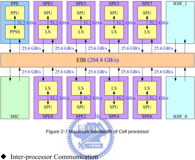
The EIB’s maximum data bandwidth is limited by the rate at which addresses are snooped across all units in the system. The rate is one address per bus cycle. Each snooped address request can potentially transfer up to 128bytes, so in a 3.2GHz Cell processor, the theoretical peak data bandwidth on the EIB is 128 bytes * 1.6 GHz = 204.8 Gbytes/sec. The maximum bandwidth of Cell processor is summarized in Figure 2-7. However, the actual data bandwidth depends on several factors: the relative locations of destination and source, the new transfer’s interferences with in-flight transfers, and the efficiency of data arbiter, etc.
LS SPU SPE1 LS SPU SPE3 LS SPU SPE5 LS SPU SPE7 SPU LS SPE0 SPU LS SPE2 SPU LS SPE4 SPU LS SPE6 PPU PPSS PPE MIC IOIF_0 IOIF_1
EIB
(204.8 GB/s)
25.6 GB/s 25.6 GB/s 25.6 GB/s 25.6 GB/s 25.6 GB/s 25.6 GB/s 25.6 GB/s 25.6 GB/s 25.6 GB/s 25.6 GB/s 51.2 GB/s 51.2 GB/s 51.2 GB/s 51.2 GB/s 51.2 GB/s 51.2 GB/s 51.2 GB/s 51.2 GB/s 51.2 GB/sFigure 2-7 Maximum bandwidth of Cell processor
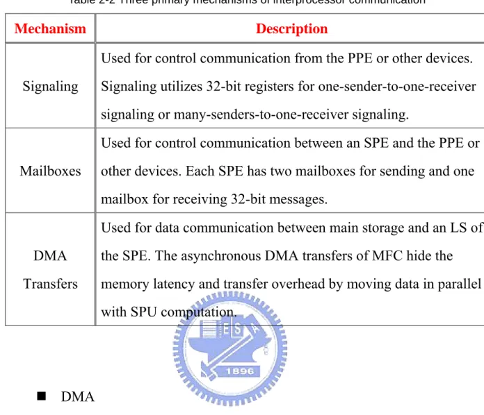
Inter-processor Communication
There are many attributes of the shared-memory system. The PowerPC processor element (PPE) and all synergistic processor elements (SPEs) have coherent access to the main storage. All communication mechanisms are implemented and controlled by the SPE’s memory flow controller (MFC). The SPEs must explicitly use the following three communication mechanisms: DMA transfers, mailbox messages, and signaling messages in order to communicate with other bus elements in the system. Table 2-2 summarizes the three mechanisms mentioned above.
Table 2-2 Three primary mechanisms of interprocessor communication
Mechanism Description
Signaling
Used for control communication from the PPE or other devices.
Signaling utilizes 32-bit registers for one-sender-to-one-receiver
signaling or many-senders-to-one-receiver signaling.
Mailboxes
Used for control communication between an SPE and the PPE or
other devices. Each SPE has two mailboxes for sending and one
mailbox for receiving 32-bit messages.
DMA
Transfers
Used for data communication between main storage and an LS of
the SPE. The asynchronous DMA transfers of MFC hide the
memory latency and transfer overhead by moving data in parallel
with SPU computation.
DMA
An MFC supports naturally aligned DMA transfer sizes of 1, 2, 4, 8, and 16 bytes and multiples of 16 bytes. For naturally aligned 1, 2, 4, and 8-byte transfers, the source and destination addresses must have the same 4 least significant bits (LSB). A single DMA command could transfer up to 16 KB between an LS and shared memory storage.
The throughput of a DMA transfer when the source and destination addresses are 128-byte aligned is double as compared to that of a mis-aligned transfer within a cache line. It’s because that the mis-aligned transfer is a partial cache-line transfer, and actually there may be two bus requests for this transfer. Peak performance is achieved when the size of the transfer is a multiple of 128 bytes and both the effective address (EA) and the local store address (LSA) of the DMA transfer are 128-byte aligned. The following performance guidelines for DMA commands in CBE could be made.
• Minimize small transfers
• Align source and destination addresses to a 128-byte cache-line boundary.
• Minimize the use of synchronizing and data-ordering commands.
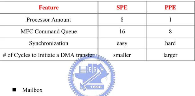
• Have SPEs (not PPE) initiate DMA transfers. The reasons state in Table 2-3.
Table 2-3 The reason why we have SPE initiate DMA commands
Feature SPE
PPE
Processor Amount
8
1
MFC Command Queue
16
8
Synchronization easy
hard
# of Cycles to Initiate a DMA transfer
smaller
larger
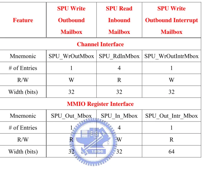
Mailbox
Mailboxes take charge of the 32-bit messages between an SPE and other devices. There are three mailbox channels of each SPE: two one-entry mailbox channels and one four-entry mailbox channel. The SPU Write Outbound Mailbox and the SPU Write Outbound Interrupt Mailbox which belong to one-entry mailbox channels are used for sending mails from the SPE to the PPE or other bus elements. The SPU Read Inbound Mailbox which belongs to four-entry mailbox channel is used for sending messages from the PPE or other bus elements to the SPE. Table 2-4 gives details about the mailbox channels and their associated MMIO registers.
Table 2-4 The mailbox channels and their associated MMIO registers
Feature
SPU Write
Outbound
Mailbox
SPU Read
Inbound
Mailbox
SPU Write
Outbound Interrupt
Mailbox
Channel Interface
Mnemonic SPU_WrOutMbox SPU_RdInMbox SPU_WrOutIntrMbox
# of Entries
1
4
1
R/W W R
W
Width (bits)
32
32
32
MMIO Register Interface
Mnemonic SPU_Out_Mbox
SPU_In_Mbox SPU_Out_Intr_Mbox
# of Entries
1
4
1
R/W R W R
Width (bits)
32
32
64
2.2 Programming on PPE and SPEs
Figure 2-8 shows the application programming interface (API) of DMA utilized in this thesis and the associated direction. The SPE could use the API “mfc_write_tag_mask” and “mfc_read_tag_status_all” to wait for the completion of DMA commands. It’s noted that the waiting time of DMA commands could be reduced by programmer, because the operation of DMA and the computation of SPU are asynchronous.
Figure 2-8 The API of DMA
Figure 2-9 shows the API of mailbox utilized in this thesis and the associated direction. The PPE could use the API “spe_out_mbox_status” to gather the information of SPU Write Outbound Mailbox for each SPE. Usually this API is bundled with “spe_out_mbox_read”. PPE use “spe_out_mbox_status” to wait the update of SPU Write Outbound Mailbox and receive the message via “spe_out_mbox_read”.
PPE spe_in_mbox_write spe_out_mbox_read SPE 1 spu_read_in_mbox spu_write_out_mbox spe_in_mbox_write spe_out_mbox_read SPE 6 spu_read_in_mbox spu_write_out_mbox spe_out_ mbox_status Mailbox Mailbox …… …… spe_out_ mbox_status
Figure 2-10 shows a common form of program which utilizes the PPE and SPEs on CBE. The communication between PPE and SPEs is a significant factor of the system performance, namely, the mailbox and DMA commands. It’s noted that the algorithm of application is almost unchanged. The major works are the function offload of SPE’s code and the building of communication scenario.
/*Initialization of SPE program*/
for each SPE, Initialize SPE;
create_spe_context;
/*Activate the computation on SPE*/
for each SPE, send input parameters;
spe_in_mbox_write(SPEid, control); spe_in_mbox_write(SPEid, I/O_address); /*Commit the completion on SPE*/
for each SPE, check output and commit;
spe_out_mbox_read(SPEid);
initialization;
/*Get input parameters*/
control = spu_read_in_mbox();
I/O_address = spu_read_in_mbox(); /*Get input data*/
mfc_get(input_LS_addr, I_address);
computation(control, LS_addr);
/*Give output data*/
mfc_put(output_LS_addr, O_address); /*Inform PPE about the completion*/ spu_write_out_mbox(COMPLETE);
Figure 2-10 The cooperation of PPE and SPEs
It’s noted that the APIs used here are mentioned above. As shown in the pseudo code the PPE maintains the thread-control and I/O behavior, and SPEs take charge of the computing tasks. The starting and ending of computation on SPEs are activated by the mails between the PPE and the SPEs.
The PPE is the manager of threads, and it creates the context for SPE. The program for SPEs would be loaded and executed in this simplified step. Then the SPEs run to the waiting for mails from the PPE. SPEs get what they want via mailboxes or DMA transfers from PPE.
The completing message would be send to PPE when the computing on SPE is done. The PPE receives this completing message and knows that the SPE with SPEid is idle and ready for next task.
3 Frame-based Data
Partitioning on CBE
This chapter focuses on the data management of multimedia stream on multi-core system. The platform is CBE, and the demonstration software is JPEG decoder. For a multi-core processor, the data communication efficiency is a key factor of the overall performance. Although the algorithm optimization and the special instruction of processor could improve the system computing power, they are too specific and irrelevant to the architecture and design concepts of multi-core. High performance can’t be achieved without the optimization of data partitioning and dataflow on a multi-core processor.
3.1 Port the Multimedia Applications to CBE
For Cell, such a multi-core processor, a common flow of porting multimedia application could be summarized as in Figure 3-1. At the beginning, a single-thread program is the most original program in the first implementation. In this original program on the PPE, the programmers could access all 264 memory address and the program runs sequentially. The
main purpose of the original program is to verify the functionality. It has a little chance to meet the performance requirements of multimedia applications nowadays without optimization.
sequential program
single-thread program on PPE multi-thread program on PPE vectorized multi-core program function offload multi-core program on PPE and SPEsoptimized program vectorization dataflow optimization parallelization
parallel program
Figure 3-1 Port the Multimedia Applications to CBE
The program could be divided into threads and then becomes a multi-thread program. This parallelization step should be done in a very careful way. In order not to reduce performance, the threads should be load-balanced. In other words, the computing time of each thread should be kept as close as possible. The processor core could then manipulate the threads equally and easily. For advanced single-core processors, the multiple functional units
(FUs) in the processors could take charge of different threads simultaneously which is called simultaneous multi-thread (SMT) processors. This approach exploits the thread-level parallelism (TLP) to boots the performance by parallel processing among FUs.
For CBE, the threads could be allocated to the SPEs [6][21]. It’s noted again that the SPEs are the computing engines in CBE. In this stage, the load-balanced threads which found previously get significance. The SPEs are all homogeneous with same computing power. Thus the threads should have equal computing time to achieve the balanced loading. There are 6 available SPEs in PlayStation 3 which in turn means that the number of load-balances threads could be 6. This technique is called “function offload” and the key point is load balancing. After function offloading, the multi-thread program becomes the multi-core program and each thread on different processors runs in parallel [22][23].
There are commonly used optimizations, namely, single instruction multiple data (SIMD) [17][18][19] and loop unrolling. This process vectorizes the code to exploit the data-level parallelism (DLP) and instruction-level parallelism (ILP). The vectorized program executes on multiple data in a single instruction (SIMD) or consumes multiple instructions with multiple functional units (FUs). The vectorization is a technique to reduce the computing time of a single processor. In a load-balanced multi-core environment, the amount of performance improvement in single processor by vectorization equals that in entire multi-core system. For example, the 200% improvement gained from SIMD in single processor core within a multi-core system, the overall maximum improvement of the entire system would never exceed 200%. Even worse, the improvement of computation in a multi-core system would be bounded by the communication between each processor core. The communication scenario is a very important performance factor in multi-core system with limited communication resource such as CBE.
The last step is to make a good dataflow plan to reduce the communication overhead within the CBE. This stage could boot the performance a lot while the bandwidth of
communication resource is low. For example, if all components connect to a low bandwidth bus, all traffic would appear in this single bus. The components wait for the data transfers to continue their own computing tasks. In the worst case, component A could wait for all other transfers until the last for itself. Then component B needs the computation result and would wait even longer. The communication overhead would accumulate if there is a traffic jam in the system. This thesis would utilize the frame-based data partition method and optimize the dataflow to reduce such burden. After the effort from programmers, the resulting optimized program is a vectorized program utilizing multi-core processor and running in parallel.
Processor 2
Processor 3
Processor 4 Processor 1
Task1 Task2 Task4
Task6 Task3 Task5 Data 1 Data 3 Data 2 Data 4 Data 4 Data 3 Data 2 Data 1
Data Partitioning
Functional Partitioning
Processor 1 Processor 3 Processor 2 Processor 43.2 Functional Partitioning and Data Partitioning for
Multi-Core Processor
Intuitively, there are two ways to partition applications over a multi-core environment, i.e., data partitioning [8][9] and functional partitioning [10][11][12] as illustrated in Figure 3-2. The left hand side of Figure 3-2 is function partitioning. A function is decomposed into tasks, and tasks are grouped and allocated to single core of the processor. The right hand side of Figure 3-2 is data partitioning. For example, we can divide a picture into partitions and process each partition on a single processor. For a streaming application running on multi-core processor, the bottleneck of system performance is generally determined by the communication between each core.
The locality of data plays an important role in such an environment. At first, data should be loaded to a local memory. Then all operations are performed at local processor. Finally, the result is transferred back to the shared memory at higher level. The input and output data packets flowing into the local processor and the intermediate results should be no larger than the comparatively small size of local memory. When the small local memory is occupied by data and instruction together, and the application deals with large data sets and performs complex algorithm, the data partitioning and management becomes a big challenge.
3.3 Comparison between Data and Functional
Partitioning
partitioning. Some comparisons could be made between data and functional partitioning [8].
•Depending on the application, different approaches result in different communication behavior. For data partitioning, communication overhead would occur because of the data dependencies between the partitions; for functional partitioning, communication overhead would occur between individual tasks on different processor cores.
• In the case of data partitioning, task-to-task communication remains locally on the core if sufficient local memory size is available. Thus, data partitioning inherently results in locality of data.
•It’s very common that the number of data partitions is larger than the number of processor cores. Given sufficient data partitions, load balancing between processor cores comes in a nature way; for functional partitioning, it’s not uncommon that a certain task becomes a system bottleneck due to imbalanced loads of the processor. It strongly depends on the granularity of the functional decomposition into tasks and takes a lot of work to find a clear balanced partitioning point.
• Data partitioning provides scalability of software. For instance, a Standard-
Definition (SD) multimedia sequence can be decoded using 2 CPUs, whereas for HD resolution 8 CPUs are needed. For functional partitioning, different throughput requirements would affect the overall partitioning of the application, which results in laborious rewriting of the software.
• In order to fully exploit the computational power of the specific processors chosen by programmer, the application software needs to be optimized for instruction-level parallelism. For functional partitioning, this purpose would take a great deal of effort in the way of partitioning and the restructuring the software; for data partitioning, the partitioning remains unchanged, since each processor cores executes the complete function. The comparison is summarized in Table 3-1.
Table 3-1 Data partitioning vs. functional partitioning
Feature Data
Partitioning
Functional Partitioning
Communication
between Partitions
data dependency
task dependency
Load Balancing
nature balance need
extra
effort
Scalability good
bad
Optimization
partitions remain
unchanged
re-partitioning
The main issue that needs to be resolved for data partitioning, is the minimization of the communication overhead for data dependencies between partitions. Furthermore, the scheduling of the data partitions has to be considered, since inter-dependencies impose restrictions on the order in which the partitions can be processed. The best way is making the data partitions fully independent, although there should be a cost of occupying a room on shared memory. This is the concept we proposed on a desk-top level system like PlayStation3. It is obviously that the advantages of data partitioning would become larger when the application is very complex and the amount of processing data is huge. It’s just the case while the multimedia coding standard becomes more aggressive with time goes by.
3.4 The Partitioning and Management of Multimedia
Decoding on CBE
First of all, the decision about what should be left in SPE and what should be left in PPE must be made. The usual and recommended way is to move all computing part of an
application to SPE and leave the memory management part and system control task in PPE. The most computing-intensive part is the decoding algorithm, so it is reasonable to put all decoding function into SPE. For the input process, such as file reading, data packet management and the formation of one frame should be put into PPE. The display process, usually the last step in real time multimedia decoding, utilizes the frame buffer of shared memory in PS3. This is absolutely a PPE task which manages memory and the peripheral.
The way of data management between encoded multimedia stream and decoded multimedia frame is an important issue, especially when the local store (LS) is comparatively too small for the stream or frame. The smoothness of dataflow is a basic requirement for high performance and must be treated carefully. It’s depicted in Figure 3-3. Thus the design of dataflow and allocation of buffers become the major concern in this chapter [16].
Figure 3-3 The situation of LS in the multimedia decoding
For SPE, the program and data both reside in a single 256 Kbytes LS, so the usage of program memory earns the first glance. Thus the starting work is to minimize the code size of which part would be placed into the SPE. This means that the loop unrolling and some other techniques which trade the code size for the performance should not be used before the porting on SPE.
After some surveys of open source code, we insure that the algorithm part in the program of simple multimedia decoder usually would not excess the limited size of the LS. Typically the resulting execution file with no compiler’s optimization on SPE is about 130 Kbytes. It’s worthy to note that the CBE SDK provides a mechanism called “SPU Overlay” to support the access of SPU overlay code sections located in the main memory. It can decompose the large code into small segments and load with programmer’s will. However, this mechanism degrades the performance due to the overhead of the loading of the code sections. Next, the consideration moves from program to static data on SPE.
There is an amount of static data in the program of multimedia stream codec. Take JPEG for example, the quantization table and the Huffman tree table are necessary. For the quantization table, the luminance table and chrominance table are needed. For the Huffman tree table, the luminance DC and AC table, the chrominance DC and AC table are needed. Furthermore, the code lookup table and the code size table should be built from the above Huffman tree table and the header information. The total size of tables used in JPEG is summarized below:
Table 3-2 Total size of table used in JPEG
unit: bytes
Luminance Chrominance
Total
Table DC AC DC AC
Quantization 64*1
64*1 128
Huffman Tree 16+12 16+162 16+12 16+162
412
Huffman Code 512*2
512*2 512*2
512*2 4096
Huffman Size 512*1
512*1 512*1
512*1
2048
Total 792 792
6684
There are still some heap data in the program. The heap size should also be minimized by the programmer. However, heap data is highly application-dependent and not the significant part of the local store. Thus the important thing of the programming in CBE is to keep the size of program and heap small. In the roadmap of CBE, the size of LS may be enlarged with the improvement of semiconductor technology. It’s good news for the methodology of data partitioning. The programmers are more comfortable for the larger LS because that the more processing data units could be pulled in and out from the shared memory each time.
SB #1
SB #2
DC coefficient
of DCT
AC coefficients
of DCT
SB #3
SB #4
SB #1
SB #2
SB #3
SB #4
MB #1
MB #2
Figure 3-4(a) Data dependency in JPEG
current
MB
Intra
MV
Deblock
Intra
MV
Intra
MV
Deblock
Intra
MV
Dependency for the current MB:
Intra → intra-prediction
MV → motion vector prediction
Deblock → deblocking filter
Figure 3-4(b) Spatial data dependency in H.264
as described in section 2.2. The MB could be partitioned into sub-block. There are many dependencies between MBs and/or sub-blocks. Figure 3-4 shows two examples. In the simple case of JPEG, the DC value in DCT of this sub-block comes from the DC value of the previous sub-block and the difference value which is encoded in this sub-block. Furthermore, in H.264 the spatial data dependencies are the left, upper left, upper, and upper right MBs. A total of 4 reference MBs are involved in the decoding of this MB. This dependent data should keep in the LS until it’s useless to avoid the massive data reloading from the shared memory. This is a very critical step after the minimization of program and static data. The number of times of DMA in the multi-core system should be as small as possible. After the first compilation of application, the remaining room in LS should be smartly utilized with these basic data units.
In multimedia decoding the input is in the form of stream, and the variable length encoding scheme makes the parallel processing at input very difficult. For data partitioning technique, the parallel processing is at data level. To fully utilize the parallelism that data partitioning has, the data level parallelism should be shift to a level higher than MB. The appropriate level of data parallelism is frame-level, and only in this way the variable length decoding could be put into SPE. The entire decoding functions are now in SPEs, and the input and output data management left in PPE as expected.
Move from the single PPE program to the SPE program, the MB-based multimedia decoding algorithms are unchanged. The only difference is that SPEs cannot directly access the shared memory. The shared memory of all system could be accessed by SPEs only with the help of DMA. The scenario of data communication between each LS in SPE and the shared memory is shown in Figure 3-5. The partitions at shared memory are divided into 2 categories: the multimedia stream and the frames. The partitions at LS are divided also into 2 categories: the input buffer and the output buffer. It’s noted that there are still program and data storage in the LS which is not shown in the figure. The I/O buffer utilized the remaining
part of LS as described above. SPE reads the multimedia stream with input buffer and write to the frame through output buffer. The reading and writing process between the LS and shared memory carries out through DMA command (dashed lines in Figure 3-5). For decoding of one frame, the I/O process at SPE runs many times because the size of multimedia stream and frame is much bigger than the I/O buffer in size. Each SPE takes charge of the decoding of one frame. The stream of one frame is represented as many chunks. Each chunk has the size which equals the size of input buffer. Put it in another way, the input stream of one frame is cut into pieces by the input buffer. Input buffer gets one piece per DMA command. The relationship between output buffer and the frame in shared memory is similar. The details of dataflow and buffer allocation are discussed in following sections.
A basic multimedia decoding flow is placed in the SPE part of the figure. Variable length decoding is the 1st function of decoder. The implementation of variable decoding often involves lookup tables which must be stored in LS. The 2nd function is inverse quantization which is very common in many multimedia applications and involves quantization tables. The 3rd function is inverse transformation which is usually a type of inverse discrete cosine transformation (IDCT). The final function is color space transformation for the purpose of display. The transformation from YCbCr to RGB is the most common color space transformation being used. For advanced multimedia application, there would be more functions between inverse transformation and color space transformation. The complexity of a multimedia decoding algorithm largely depends on the processes in this interval. However, the complexity and optimization of multimedia decoding algorithm are not the concern and discussion in this article, i.e., the performance of decoding on a single core is not the issue here. The focus is the data partitioning and dataflow planning for multi-core system.
3.5 Dataflow Planning for Multimedia Decoding on CBE
of multimedia stream into encoded frame and dispatch to each The proposed dataflow planning for frame-based multimedia decoding on Cell is summarized in Figure 3-6 below. Start from the input multimedia stream and end at the display of frames. Partitioning
SPE is the first task of PPE.
The encoded frames in a multimedia stream are divided into groups. There are 6 frames in each group. The reason why the number “6” is chosen here is obvious: there are 6 available SPEs in PS3. The encoded frames are allocated to SPEs in a round-robin fashion, i.e., the frame 1, 7, and 13… are allocated to SPE 1, the frame 2, 8, and 14 are allocated to SPE 2, … etc. It should be noted that the actually data size flowing in and flowing out of a single SPE
depends on the I/O buffer in LS. An entire frame cannot be pulled in or out the LS once a time undoubtedly. Thus the I/O buffering is a significant issue in the design of multi-core
rogramming. This would be discussed in section 3.6. p
1 2 3 4 5 6 7 8 9 10 11 12 13
SPE 1 SPE 2 SPE 3 SPE 4 SPE 5 SPE 6
PPE
encoded frame#
1, 7, ... 2, 8, ... 3, 9, ... 4, 10, ... 5, 11, ... 6, 12, ...decoded frame#
PPE DMA DMAfile
Frame Buffer 14monitor
Figure 3-6 Dataflow planning for multimedia decoding on Cell
The decoding mechanism needs 6 frame repositories in shared memory. Each SPE utilizes its own frame repository thorough all decoding of frames. Each frame repository occupies one RGB frame in size. The content in frame repository could be updated right after the display of current frame. In some aggressive multimedia decoding standards such as H.264, the data communications would cross the frames, i.e., inter-prediction or motion
compensation. In such case this decoding mechanism needs 6 larger repositories in shared memory to accommodate the longer range of data dependency. It is feasible in desktop-level
PPE takes charge of the frames’ movement from the 6 frame repositories to the frame buffer.
3.6 DMA and Buffer Allocation on CBE
MA size is shown in the n
e half ring oundary, and the access of this ring structure could be simply in a smooth way.
computers such as PS3.
Finally the display process takes each frame from 6 repositories also in round-robin and shows the frame on the monitor through the frame buffer in PS3. The
For MFC of SPE, the transfer size of a single DMA command ranges from 1 byte to 16 K bytes. It would be a confusing problem for programmers to decide on how large the size should be with DMA commands. Therefore, the beginning of optimization is the transfer size per DMA command. We keep the size of input and output buffers constant and tune the transfer size of DMA commands. The detail of experiment on different D
ext chapter. Now, the buffer allocation and structure is considering.
The processing of each code is variable in length, thus a basic implementation is to read one byte from the input stream each time until the code is valid. This method is feasible on a single core system undoubtedly, but it’s dangerous for the multi-core system where massive data communication holds. For CBE the DMA is not efficient enough. To get one byte each time from the input stream at shared memory is a huge burden and would become one performance bottleneck. This would be shown in the next chapter. Thus input buffer is implemented as a ring structure as shown in Figure 3-7 and read from the file block-wise. Now the reading of one byte each time accesses the input buffer in LS, not the shared memory through DMA. The term “ring” means that the data in buffer is continuous across th
circular
input buffer
DMA
SPU
16K bytes
Figure 3-7 The input buffer is a ring structure
educed. It’s a common case because that the MB size is usually not more than tens of by
procedure could simply be viewed as a decompression of a tightly comp
It’s noted that the update of half ring is an input DMA command that could occur anywhere depending on where the boundary checking and update places. The simplest way of boundary checking and update is to check right after each reading of input buffer in LS. However the boundary checking and update could be move to a bigger block, namely, the MB. It could be placed where the processing of one MB is complete. In this way the size of half ring must be larger than the size of one MB in bytes, and the number of boundary checking could be r
tes.
For a decoding application, the output bandwidth is many times larger than input bandwidth. The decoding
ressed data stream.
Because multimedia decoding is a MB-based algorithm, the output basic unit is MB. The MB size commonly used is 16*16 = 256 points. Thus the output size is 256*3 = 768 bytes if the red, green and blue colors are stored as 1 byte each (256 levels). There are 16 rows and 16*3 = 48 columns in one output MB. For a single DMA command, the access address should be consecutive. To be more specific, the DMA command contains only the starting address
and the access size in bytes. The size of a single DMA command for output is set at 128 bytes. The packing of pixels for display is done on PPE. The typical form of output buffer for MB-based multimedia decoding algorithm is shown in Figure 3-8. The term “n macroblocks” in the figure means the width of the output buffer in terms of the number of MBs. There are 16 pixels in each row of one MB, i.e., 48 bytes in each row for RGB 3 colors. The discussion
f how to set “n macroblocks” is left in the next chapter. o
……
……
Figure 3-8 The single output buffer
double-buffering case, which MFC and SPU utilize buffer A and buffer B interchangeably.
An improvement at output buffer could be made in this decoding scenario. The double buffering is a technique to overlap the data transfer and the computation: the current result is written to one buffer by SPE, while the previous result residing in the other buffer is sent to the shared memory through DMA. The difference between the single buffering and double buffering is shown in Figure 3-9. “MFC” refers to the memory flow controller and “SPU” to the synergistic processing unit as mentioned in Chapter 2. SPU is busy at decoding while MFC is busy at output DMA commands. There are two buffers in the
SPU MFC decoding 1 (buffer A) DMA 1 (buffer A) decoding 2 (buffer A) DMA 2 (buffer A) time decoding 3 (buffer A) DMA 3 (buffer A) decoding 4 (buffer A) DMA 4 (buffer A)
Figure 3-9(a) Single buffering
Figure 3-9(b) Double buffering
However, there are 2 situations in which the effects of double buffering are not so attractive. Namely, the 2 asynchronous processes are very imbalanced in consuming-time. These situations are shown in Figure 3-10. In Figure 3-10(a), the computation time of SPU is much less than the DMA time of MFC. This is what this thesis focuses on. It is noted that the DMA time of the multi-core system increases in a multiple trend with the number of cores. There are 6 SPEs in CBE, and the DMA time should be 6-fold as compared to 1 SPE. The total system performance is bounded if the DMA time is much larger than the computation time, i.e., the utilization of 6 SPEs couldn’t have 6-fold speedup as compared to that of 1 SPE. This is the critical problem which must be solved in the multi-core system. The DMA and the associated buffer allocation would be discussed in the followings.
The other situation is shown in Figure 3-10(b), where the computation time of SPU is much more than the DMA time of MFC. This situation is solved by the optimization of decoding algorithm and the utilization of chosen processor. The commonly used techniques are single-instruction-multiple-data (SIMD), loop unrolling, and some special extended
instructions. It’s not the point discussed here.
Figure 3-10(a) The computation time of SPU is much less than the DMA time of MFC
SPU MFC decoding 1 (buffer A) decoding 2 (buffer B) time decoding 3 (buffer A) decoding 4 (buffer B) DMA 1 (buffer A) DMA 2 (buffer B) DMA 3 (buffer A) DMA 4 (buffer B)
Figure 3-10(b) The computation time of SPU is much more than the DMA time of MFC
11. here are 2 pairs of data movement depicted as the arrows. Pair A is the upper left and the bott
t wraps around and starts at the beginning of ring. The ring buffe
The implementation of double buffering for multimedia decoding is shown in Figure 3-T
om right arrows and Pair B is the upper right and the bottom left arrows. These 2 pairs take place in a ping-pong fashion, and the computation and DMA could utilize 2 buffers respectively at the same time.
The 2 halves of input ring buffer operates cooperative. When the address of this ring buffer excesses the total size, i
half which is non-accessed updates by reading half size of data from the input stream. The basic unit of the size of input ring buffer is 128 bytes. The reason and the associate discussion are provided in Chapter 4.
output buffer in LS # MBs SPU DMA
……
……
output buffer in LS……
……
A A B BFigure 3-11 The I/O double buffer
The double buffering ma ers are asynchronous to SPE omputation. It’s noted that this technique double increase the output buffer size. There may be a
tches the property that DMA transf c
situation that double buffering isn’t feasible in such limited LS in SPE. It’s a tradeoff issue of memory storage and the performance.
4 Experimental Results
This chapter provides the experimental results of different size of DMA transfers and the allocation of I/O buffer. The experimental environment is shown below.
Instrumentation PlayStation 3
Linux kernel: 2.6.16 (Fedora) [14] HD monitor
System input
1080p motion JPEG sequence System output
1080p decoded frames displayed on monitor
The code structure of experimental program is shown in Figure 4-1. The PPE controls the decoding task on each SPE, and the SPEs take charge of the decoding of frames. The PPE first create the spe_context for each SPE to start the running of SPE program. SPE freely runs to the location waiting for the I/O address from PPE. The PPE sends the I/O address to SPE
needed for the decoding of one frame. The SPE continues computing after the reception of mail from PPE. When the decoding task is done the SPE sends a mail to PPE informing about the completion. The PPE display the decoded frames after the reception of completion mail and send another I/O address to the idle SPE. The detail operation for PPE and SPE side is made below.
At first, the PPE side is considered. PPE accumulates 6 encoded frames from the input stream and allocates them to 6 different SPE threads. The PPE mail the memory pointers of 6 encoded frames and the 6 frame repositories to individual 6 SPEs. After this initial sending of response is the completion mail sent by SPE to PPE. When PPE knows the decoding of one frame is done, the display procedure follows.
The display procedure fills the RGB color pixels into the frame buffer of PS3 system. This
part of multimedia
frame, the returned SPE which completes its decoding gets another ntinues on the decoding job activating by this
ll frames need to be decoded, PPE waits for another comeback of one SPE ll frames are sent to SPEs, PPE goes to the final step. pletion mail from all SPEs and display the last frames. The overall mails PPE waits for the response of one SPE. The actual meaning of
procedure takes about 1/120 seconds per 1920*1080p frame. Thus the display procedure would only slightly degrade the performance and not be the critical
decoding.
After the display of
encoded frame pointer. The returned SPE co mail from PPE.
If there are sti
and repeats the flow described above. If a PPE waits the com
decoding ends.
As for the SPE side, SPEs could be viewed as servants of PPE. The practical implementation in SPE is an infinite loop starting from the reception of mail and return to the loop at the sending of completion mail. SPEs get the mail containing the input encoded frame pointer and the output decoded frame pointer from PPE. Then SPE knows where to get the
input and put the output in shared memory. SPE starts running the decoding function when the PPE sends this information to it. At the end of decoding of one frame SPE sends a mail to PPE to tell PPE the completion.
PPE side
/*Display initialization*/
for each SPE, initialize SPE;
n SPE*/ meters to SPE; spe_out_mbox_read(SPEid); /*display on monitor*/ me buffer(resolution); wait_for_vsync;
SPE side
initialization; while(1) {for each macroblock in one frame {
mfc_get(input_LS_addr, I_address);
decoding process(LS_addr); spu_write_out_mbox(COMPLETE); } fd = open_device; get_screen_info; get_fb_control; read file;
/*Initialization of SPE program*/
create spe_context;
/*Activate the frame decoding o for each frame, send input para
/*Get input parameters*/
I/O_address = spu_read_in_mbox();
/*Decoding process*/ /*Get input data*/
spe_in_mbox_write(SPEid, I/O_address);
/*Commit the decoding completion on SPE*/ for each frame, commit and display;
fill fra
/*Give output data*/
mfc_put(output_LS_addr, O_address);
}
/*Inform PPE about the completion*/
output the content in fb;
Figure 4-1 The code structure of experimental program
The frame buffer is a double buffer and it could be viewed in 3 layers. The first layer is application layer which is controlled by programmers at top level. The control registers could be modified by users manually to enhance the controllability of frame buffer. The performance is improved by this way without the usage of application programming interface (API). The second layer is kernel layer which is handled by operating systems (OS). The communication and operation mechanisms between Cell processor and graphic processing unit (GPU) are automatically controlled by kernel. The frame buffer is a virtual memory, and
it’s managed by kernel. The third layer is GPU layer which is the heart of graphic computing and display. There are double frame buffer in GPU, and the content is delivered by kernel via DMA. GPU provides the display on monitor. The schematic of these 3 layers is shown in
igure 4-2. F
Application
K
GPU
ernel
decoder
frame buffer 0
on XDR
frame buffer 1
on XDR
Monitor
frame buffer 0
on GPU
frame buffer 1
on GPU
A
A
A
B
B
B
Figure 4-2 The double frame buffer
The arrows A and B represent the double buffering operation mechanism. When application is busy writing results to frame buffer 0 on shared-memory (Rambus, XDR), the frame buffer 1 on XDR moves its content to frame buffer 1 on GPU via DMA, and the pixels displayed on monitor comes from frame buffer 0 on GPU. Then the frame buffer flips to the other one and follows the mechanism described above. It’s noted that the computing time of
display isn’t included in the decoding statistics below.
There are 3 optimization techniques applied in this thesis. They are vectorization, parallelization, and dataflow optimization. The performance with combinations of these techniques is shown in Figure 4-3. The unit of y-axis is frames per second (fps), and the
-axis represents the optimization techniques. x
10
20
30
40
0
50
60
70
80
90
fps
Original Parallelization Parallelization Dataflow Opt.
100
110
52.3 5.1 4.7 46.8 Parallelization Vectorization Vectorization Parallelization Vectorization Dataflow Opt. 108.9 10.0Figure 4-3 The performance with combinations of optimization techniques
The experiment is divided into 4 categories as the followings. The transfer size per DMA command
The size of I/O buffer The double buffering