This content has been downloaded from IOPscience. Please scroll down to see the full text.
Download details:
IP Address: 140.113.38.11
This content was downloaded on 28/04/2014 at 07:21
Please note that terms and conditions apply.
Temperature and Annealing Effects on Photoluminescence Spectra of (InAs)1/(GaP)2
Superlattices Grown by Solid-Source Molecular Beam Epitaxy
View the table of contents for this issue, or go to the journal homepage for more 2000 Jpn. J. Appl. Phys. 39 L968
(http://iopscience.iop.org/1347-4065/39/10A/L968)
Part 2, No. 10A, 1 October 2000 c
°2000 The Japan Society of Applied Physics
Temperature and Annealing Effects on Photoluminescence Spectra of (InAs)
1/(GaP)
2Superlattices Grown by Solid-Source Molecular Beam Epitaxy
Yi-Cheng CHENG∗, Sien CHI, Shu-Tsun CHOU1and Kai-Feng HUANG2
Institute of Electro-Optical Engineering, National Chiao-Tung University, Hsinchu, Taiwan 300, Republic of China
1Compound Semiconductor Technologies Inc., Huko, Taiwan 303, Republic of China
2Electro Physics Department, National Chiao-Tung University, Hsinchu, Taiwan 300, Republic of China
(Received June 28, 2000; accepted for publication August 4, 2000)
Anomalous variation of photoluminescence (PL) wavelengths with temperature was observed in (InAs)1/(GaP)2 short-period-superlattice (SPS) quantum wells grown by solid-source molecular beam epitaxy with different phosphorus and arsenic cracker temperatures. We believed that the anomalous PL behavior could be attributed to the multi-axial strain effect existed at the abrupt InAs and GaP interfaces in the SPS structure. After rapid thermal anneal (RTA) treatment, the anomalous PL spectra in the low temperature region disappeared but the high temperature PL characteristics remained, which revealed the thermal stability of the (InAs)1/(GaP)2quantum well structures and its potential in replacing InGaAsP quaternary.
KEYWORDS: multi-axial strain, SSMBE, photoluminescence, RTA, InAs/GaP
∗E-mail address: u8324541@cc.nctu.edu.tw
L968
1. Introduction
InGaAsP/InGaP material system lattice matched to GaAs offers some potential advantages over the well-established GaAs/AlGaAs system and this Al-free material system is es-pecially attractive for the production of laser diodes.1–3) Pre-viously, the optimization of InGaAsP/InGaP interface used growth interruptions that allow time for the residual group V material to be removed from the growth chamber before the epitaxy of succeeding layers begins. A long interruption time is usually needed to remove the residual species con-siderably from the growth chamber. Although an increased pause time will lead to more uniform growth fronts, the in-corporation of background impurities at the interface must be considered during each interruption. In this report, we grew (InAs)/(GaP) short-period-superlattice (SPS) quantum wells using solid-source molecular beam epitaxy (SSMBE).4–6)We expected SSMBE to provide a precise control of both Group V fluxes in the valved crackers and an exact determination of (InAs)/(GaP) compositions in the SPS structure. Our re-sults showed that the crystal quality and interface smoothness of (InAs)/(GaP) SPS layers were indeed in a good control. In addition, factors such as group V flux ratio, species and the thermal anneal effect that could affect the crystal quality were also discussed in order to get a better understanding of the growth mechanism.
2. Experimental Details
All of the (InAs)/(GaP) short-period-superlattice multiple-quantum-well (SPS MQW) layers were grown in a RIBER 32P system equipped with phosphorus and arsenic valved crackers. Based on the lattice constant of GaAs (5.6533 Å), GaP (5.4512 Å), and InAs (6.0584 Å), the thickness of indi-vidual InAs and GaP layers in the SPS structure was set at a ratio of 1:2, in order to match the lattice constant of the GaAs substrate. In the full structure, the lower confining layer is a 0.2-µm In0.5Ga0.5P. The well regions contain five quantum wells and four barriers. The barrier and the upper confining layers are In0.5Ga0.5P of 100 Å and 200 Å, respec-tively. Each quantum well contains 8 pairs of (InAs)1/(GaP)2 SPS layers which is about 80 Å thick. The growth
temper-ature for the SPS quantum well regions and cladding lay-ers is about 500◦C. All samples were characterized by vari-able temperature photoluminescence (PL) spectroscope using a helium-cooled cryostat with temperature control. The exci-tation source was the 476.5-nm line of an Ar+laser.
3. Results and Discussion
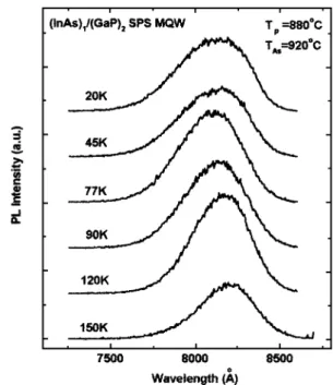
Figure 1 shows the temperature dependent evolution of PL peaks from an (InAs)1/(GaP)2SPS MQW sample, which was grown with the phosphorus and arsenic cracker temperatures set at 880◦C and 920◦C, respectively. At low measuring tem-perature from 20 to 77 K, the peak wavelength decreases grad-ually with increasing temperature. In the range between 77 and 150 K, however, the PL peak wavelength appears to in-crease continuously with increasing temperature. The shift of the PL peak wavelength from 20 to 150 K is only about 60 Å. To further understand the anomalous PL behavior shown in Fig. 1, a series of (InAs)1/(GaP)2 SPS MQW samples were
Fig. 1. Temperature-dependent PL peak wavelength of the (InAs)1/(GaP)2
SPS MQW samples with phosphorus and arsenic cracker temperatures of 880 and 920◦C, respectively.
Jpn. J. Appl. Phys. Vol. 39 (2000) Pt. 2, No. 10A Y.-C. CHENGet al. L969
the InAs layers and/or the As residue in the ensuing GaP lay-ers. Either way or both mentioned above can decrease the effective band gap energy or increase the peak emission wave-length. On the other hand, in samples A and B, higher phos-phorus cracker temperature resulted in a longer peak wave-length though the effect is not as emphatic as in the higher As temperature case. Since a higher phosphorus cracker tem-perature means a higher P2/P4 ratio, if more P2 is involved in the crystallization due to its higher chemical reactiveness, the effective band gap energy should increase instead of what was observed in the real situation. Therefore, in this case, we believe that more In incorporation should be the main cause of the longer emission wavelength observed in sample A.
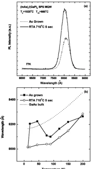
In contrast, in the low temperature region, all three samples showed almost sporadic peak wavelength variations. Since low temperature luminescence is more of a reflection of lo-calized radiative recombination, the exact compositions of adjacent regions and the interfaces in the (InAs)/(GaP) SPS structures should affect more on the luminescence property than the overall equivalent composition. Therefore, another set of samples was treated with rapid thermal anneal (RTA) method. There are two purposes for this test, the first is to check the thermal effect on the luminescence property and the second is to confirm the thermal stability of the (InAs)/(GaP) SPS quantum well structures. Figure 3 shows the comparison of PL peak intensity and temperature dependent peak wave-length measured from samples with and without the post-growth RTA treatment. These two samples were taken from the same (InAs)1/(GaP)2 SPS MQW wafer grown with the phosphorus and arsenic cracker temperatures set at 1020 and 660◦C, respectively. The ex situ RTA was performed at 710◦C for 5 s. The 77 K PL intensity and the wavelength spectra of the test sample before and after RTA were shown in Fig. 3(a). The peak intensity increased significantly after the RTA treat-ment. The wavelength experienced a slight blue shift of about 80 Å from 8095 to 8016 Å. The greatly increased PL peak in-tensity is apparently an indication of crystal quality improve-ment from the RTA treatimprove-ment. On the other hand, the slight peak wavelength shift of samples undergone RTA treatment demonstrated the thermal robustness of the (InAs)1/(GaP)2 SPS layers. Since (InAs)1/(GaP)2SPS structure has an aver-age lattice constant matched to the GaAs substrate, the strain enhanced diffusion was apparently not being an issue in our samples, and that shall be one of the key issues for the success of replacing InGaAsP quaternary with the SPS layers.
Figure 3(b) shows the temperature dependent PL peak wavelength measured from the same two samples. Also shown is the temperature dependent band gap variation of bulk GaAs resulted from the simulation.7) In the as-grown condition, i.e., without any RTA treatment, the abnormal wavelength variation in the range from 13 to 200 K is un-stable, similar to the other samples shown in Fig. 2. Af-ter RTA, the peak wavelength becomes stable. Despite their drastic difference in wavelength dependence on temperature from 13 K to 200 K, similar peak wavelengths were observed both at 13 K and 200 K. Furthermore, it is interesting to see that the RTA treated (InAs)1/(GaP)2 SPS MQW sam-ple showed a temperature dependency of the PL peak wave-length similar to bulk GaAs. The PL peak wavewave-length shift of this (InAs)1/(GaP)2SPS sample is about 270 Å from 13 K to 200 K, and that of the simulated GaAs bulk is about 290 Å
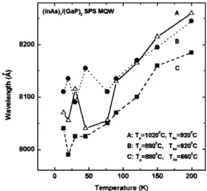
Fig. 2. Temperature dependence of the PL peak wavelength of (InAs)1/
(GaP)2 SPS MQW samples grown with different phosphorus cracker
temperature (Tp) and arsenic cracker temperature (TAs). Sample A:
Tp = 1020◦C, TAs = 920◦C. Sample B: Tp = 880◦C, TAs = 920◦C.
Sample C: Tp= 880◦C, TAs= 660◦C.
grown at different phosphorus and arsenic cracker tempera-tures, or P/As ratios.
In Fig. 2, (InAs)1/(GaP)2samples grown with phosphorus and arsenic cracker temperatures set at 1020◦C and 920◦C respectively were denoted as sample A. Those grown with phosphorus and arsenic cracker temperatures set respectively at 880◦C and 920◦C were denoted as sample B, and those grown with phosphorus and arsenic cracker temperatures set respectively at 880◦C and 660◦C were denoted as sample C. Below 90 K, all samples revealed a blue shit or decrease of PL peak wavelength with increasing temperature. When the temperature is higher than 90 K, all of the peak wavelengths increase as the temperature increases. Note that changing the P/As ratio did not prevent the appearance of the anomalous behavior, but it could affect the intensity and peak wavelength of the anomalous behavior. Since the only difference between samples A and B is the temperature of the valved phosphorus cracker, the difference observed in the PL spectra between these two samples should originate from either the variation of phosphorus flux magnitude or the P2/P4 ratio in the flux. In addition, because the difference between samples B and C is only the As temperature, the variation of the PL peak wavelength between them should originate from the As flux magnitude or the chemical reactiveness of the arsenic species involved in epitaxy.
According to our study, a higher P cracker temperature can yield a higher P2/P4 ratio in the flux and a higher As cracker temperature can also produce a higher As2/As4 ra-tio in the flux. It is well known that As2 is more chemically reactive than As4 and we expect a similar trend between P2 and P4. Meanwhile, at higher temperature, the luminescence peak usually is an indication of the overall composition in the SPS layers due to the stronger kinetic behavior of carriers that could result in more prominent thermal emission and/or tunneling effect. Therefore, the peak wavelength revealed by sample B at 200 K indicated that sample B has either a higher In content or more As incorporation than sample C. Both situations could exist if As2 is indeed chemically more re-active than As4and that can increase the In incorporation in
within the same range. The anomalous photoluminescence behavior in the low temperature range had been observed in many (In, Ga)/(As, P) structures with different growth condi-tions and systems.8–11) The cause of the anomaly had been attributed to a high degree of ordering,8)multi-axial strain dis-tribution11)or negative thermal expansion.12)However, since the RTA treated sample did not show the same behavior but a similar one to the GaAs bulk, this anomalous behavior is less possible resulting from the intrinsic negative thermal ex-pansion property. In addition, since similar peak wavelengths were observed both at 13 K and 200 K from samples with and without the RTA treatment, the ordering effect is not likely to be the cause either. Due to the anomalous behavior was observed only when the temperature was below 90 K and dis-appeared after the sample was annealed, this behavior should be more likely related to multi-axial strain effect at low tem-perature.
Considering the behavior of (InAs)/(GaP) SPS MQW structure at high temperature, its thermal expansion was bulk crystal like or manipulated by the thermal expansion of the GaAs substrate. In other words, if there is any other strain effect in the SPS structure, it will nevertheless be smeared out by the dominating substrate effect. However, at low tempera-ture, the thermal expansion of GaAs substrate is relatively not
so dominant and that gives a chance for the PL spectra to show the multi-axial strain effect occurring in the SPS layers. We believe that the multi-axial strain should be resulting from the
1) D. Z. Garbuzov, N. Y. Antonishkis, A. D. Bondarev, A. B. Gulakov, S. N. Zhigulin, N. I. Katsavets, A. V. Kochergin and E. V. Rafailov: IEEE J. Quantum Electron. 27 (1991) 1531.
2) H. J. Yi, J. Diaz, L. J. Wang, I. Eliashevich, S. Kim, R. Williams, M. Erdtmann, X. He, E. Kolev and M. Razeghi: Appl. Phys. Lett. 66 (1995) 3251.
3) W. E. Plano, J. S. Major, Jr. and D. F. Welch: IEEE Photon. Technol. Lett. 6 (1994) 465.
4) J. N. Baillargeon, A. Y. Cho and R. J. Fischer: J. Vac. Sci. & Technol. B13 (1995) 64.
5) M. Pessa, M. Toivonen, M. Jalonen, P. Savolainen and A. Salokatve: Thin Solid Films 306 (1997) 237.
6) C. C. Wamsley, M. W. Koch and G. W. Wicks: J. Vac. Sci. & Technol. B14 (1996) 2322.
7) Y. P. Varshni: Physica 34 (1967) 149.
abrupt InAs and GaP interface in the SPS structure. Due to the difference of lattice constants and thermal expansion co-efficients, a thermal stress should be generated at the interface of these two regions, although it was prominent only at low temperature but disturbed at high temperature by the substrate expansion. The anomalous PL behavior was apparently a re-flection of the existence of this thermal stress. However, this thermal stress existed only when the abrupt interface existed and would disappear when the sample was annealed which would smear out the interface. It has also been shown pre-viously that peculiar PL phenomena were possible to be ob-served in both (InAs)/(GaAs) and (InP)/(GaP) SPS layers due to the multi-axial strain effect.13) More advanced measure-ment works are need to fully understand this phenomenon.
4. Conclusions
In summary, since a high PL peak intensity was con-sistently obtained in our study and a high thermal stabil-ity was proven by the RTA treatment, we believed that the (InAs)/(GaP) SPS layers have great potential in replacing the InGaAsP quaternary. In addition, we also observed anoma-lous temperature dependent PL behaviors in the (InAs)/(GaP) SPS samples. Altering the group V species ratio did not elimi-nate this anomalous phenomenon but only vary its magnitude. However, this PL anomaly can be eliminated by thermal an-neal, since the (InAs)/(GaP) SPS sample with RTA treatment showed a temperature dependent PL spectrum similar to bulk GaAs. We believed that the anomalous PL behavior actu-ally is an evidence of the abrupt interface in the (InAs)/(GaP) SPS structure. This abrupt interface could be smeared out by the RTA treatment, but the integrity of the (InAs)/(GaP) SPS quantum well structure could withstand an annealing temper-ature as high as 710◦C. Therefore, optimized (InAs)/(GaP) SPS structures have high potential in practical devices appli-cation. More work is planned to develop a better control of the temperature dependent PL characteristics and emission wave-lengths on the (InAs)/(GaP) SPS structure.
Acknowledgements
The authors would like to thank Dr. Wen-Jen Lin and Dr. Wen-How Lan of the Chung-Shan Institute of Science and Technology for experimental assistance. This work was sup-ported by NSC (89-2112-M-009-018) of Taiwan, Republic of China.
Fig. 3. (a) 77 K PL spectra of the (InAs)1/(GaP)2SPS MQW sample with
and without RTA method. (b) Temperature-dependent PL peak wavelength of the sample shown in (a). The dash line shows the variable peak wave-length of simulated GaAs bulk.
Gonda: Jpn. J. Appl. Phys. 35 (1996) 4225.
11) D. E. Wohlert, S. T. Chou, A. C. Chen, K. Y. Cheng and K. C. Hsieh: Appl. Phys. Lett. 68 (1996) 2386.
12) H.-M. Kagaya and T. Soma: Solid State Commun. 58 (1986) 479. 13) S. T. Chou: J. Appl. Phys. 87 (2000) 285.
8) M. Kondow, S. Minagawa, Y. Inoue, T. Nishino and Y. Hamakawa: Appl. Phys. Lett. 54 (1989) 1760.
9) B. T. McDermott, K. G. Reid, N. A. El-Masry, S. M. Bedair, W. M. Duncan, X. Yin and F. H. Pollak: Appl. Phys. Lett. 56 (1990) 1172. 10) S.-J. Kim, H. Asahi, M. Takemoto, K. Asami, M. Takeuchi and S.-I.