行政院國家科學委員會專題研究計畫 成果報告
子計畫八:HBT 中頻積體電路及後製程研究(3/3)
計畫類別: 整合型計畫 計畫編號: NSC92-2219-E-002-008- 執行期間: 92 年 08 月 01 日至 93 年 07 月 31 日 執行單位: 國立臺灣大學電機工程學系暨研究所 計畫主持人: 呂學士 計畫參與人員: 林宥佐、陳春豪、楊育哲、廖芳仁、涂欣元 、 戴嘉良、 沈 致賢、江銘洲 、陳昱璋 報告類型: 完整報告 處理方式: 本計畫可公開查詢中 華 民 國 93 年 11 月 2 日
1
第一年度成果報告
一、中文摘要 本計劃中,已實現以磷化銦鎵/砷化鎵 異質接面雙極電晶體製作之匹配良好的寬 頻放大器,多迴授路徑技術亦被用來同時 達成阻抗匹配及頻寬增加。此外,從電路 的電壓增益公式中之極點位置,我們發展 出一種方法,可用來決定輸入及輸出返回 損失(或 S11/S22)的頻率響應。實驗結果發 現,此電路具有 16dB 的小訊號增益及 11.6GHz 的 3dB 頻寬,且在這頻寬之內, 輸入和輸出返回損失皆小於-10dB,這些結 果和我們用公式推導出的電壓增益,轉導 增益,頻寬及輸出入阻抗都很吻合,並且 也符合此計畫所要求的規格。此外,針對 此電路的過阻尼現象,我們也在射極加上 電容來克服。 關鍵詞:寬頻放大器,多路徑迴授,磷化 銦鎵/砷化鎵 AbstractIn this project, the realization of matched impedance wideband amplifiers fabricated by InGaP/GaAs hetero-junction bipolar transistor (HBTs) process is reported. The technique of multiple feedback loops was used to achieve terminal impedance matching and wide bandwidth at the same time. A general method for the determination of frequency responses of input/output return losses (or S11/S22) from the poles of voltage gain was also proposed. The experimental results showed that a small signal gain of 16dB and a 3-dB bandwidth of 11.6GHz with in-band input/output return loss less than –10dB were obtained. These values agreed well with those predicted from the analytic expressions that we derived for voltage gain, transimpedance gain, bandwidth, input and output impedances. Also these results are suited for the specification of this project. The intrinsic over-damped characteristic of this amplifier was proved and emitter capacitive peaking was used to remedy this problem. The tradeoff between the input impedance matching and bandwidth was also found.
Keywords: wideband amplifier, multiple feedback, InGaP/GaAs
2. Introduction
Wideband amplifiers are used in a large variety of applications, such as wireless system, instrumentation, and optical communications. Among the variety of wideband amplifiers, the Kukeilka configuration is one of the popular circuits. However, no detailed account of the performance of the InGaP/GaAs HBT wideband amplifiers with Kukeilka configuration was reported. Furthermore, the design equations based directly on the Kukeilka configuration were not given before either. In this project, we present the first demonstration of Kukeilka wideband amplifiers using InGaP/GaAs HBT process. A method to calculate the frequency responses of input/output return losses based on the poles of voltage gain is also presented.
3. Principles of Circuit Design
The schematic of the Kukeilka wideband amplifier using InGaP/GaAs HBT process is shown in Fig. 1. The input stage consists of a single transistor Q1 driving the
output stage consisting of a transistor Q2 with
local shunt (Rf2) and series (Re2) feedback.
There is also an overall shunt-series feedback loop composed of resistors Re2 and Rf1. Local
shunt feedback around Q2 gives a low
impedance at the collector node of Q2 for the
output terminal impedance matching. Then global shunt feedback is applied around this voltage amplifier via Rf1 to achieve input
matching condition. The expressions for voltage gain, current gain, input/output impedances, close-loop poles and frequency responses of S parameters are described as follows.
2 Q2a Rf2=330Ω Vout Q1 Q2b Rcc1=400Ω Rcc2=150Ω R1=50Ω R2=450Ω Re2=10Ω Ce2=1.5pF Re1=10Ω Ce1=1pF Rf1=150Ω RS=50Ω RL=50Ω VS Vcc=5V
Fig. 1. The schematic of the dual feedback wideband amplifier.
3.1 Voltage and Current Gain
The open loop circuits of the dual feedback circuit for the calculations of open loop voltage and current gain are shown in Fig. 2 and 3, respectively. From Fig. 2, the voltage gain Vout/Vin without global feedback is
given by ) 1 ( ) // // ( 2 1 2 1 2 2 1 1 f K f m L cc f m K m in out V R R R G R R R G R G V V A = ≈ ≈ − (1) where Gm1=gm1/(1+gm1Re1) and
Gm2=gm2/(1+gm2Re2). gm1 and gm2 are the
transconductances of Q1 and Q2, respectively. Here the total voltage gain is
V S in in in out S in VSF A R R R V V V V A + = = (2) where Rin is the input resistance of this
circuit with global feedback, and it will be derived later.
Fig. 2. Small signal circuit for open loop voltage gain From Fig. 3, the formula of current gain without global feedback can be obtained.
2 2 2 1 2 1 ) // ( 1 // ) ( m L cc m L cc f m e f I G R R G R R R G R R A × + + × × + = (3) Therefore the total current gain is given by
2 1 e f S S I S in in out S out IS R R R R A I I I I I I A + + = = = (4) Finally, the loop gain T can be determined by
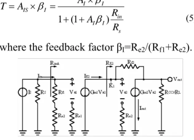
s in I I I I I IS R R A A A T ) 1 ( 1 β β β + + × = × = (5) where the feedback factor βI=Re2/(Rf1+Re2).
Fig. 3. Small-signal circuit for open loop current gain 3.2 Input and Output Impedance
By inspection of Fig. 3, the input resistance with feedback is 2 2 2 2 1 2 1 2 1 ) // ( 1 // 1 1 e m L cc m L cc f m e f I I e f in R G R R G R R R G R R A R R R + + + + = + + = β (6)
On the other hand, the output resistance can be derived directly from its definition and is given by cc K m K f cc out out R R G R R R R R // 1 // ' 2 2 2 2 + + = = (7) where Rk2 is defined as 2 2 1 1 2 1 2 e m m s f s K O K R G G R R R I V R = = + (8) and Rout’=(Rf2+Rk2)/(1+Gm2Rk2). 3.3 Close-loop Poles
Careful analysis of wideband amplifier without global feedback yields the approximation pole positions as
(
)
[
( )]
1 1 1 1 1 1 2 1 1 1 1 e f e b s e m m m P R R R r R R g g C g + + + × × + × ≈ π ω (9) ⎥ ⎦ ⎤ ⎢ ⎣ ⎡ + + × + + × × + × ≈ 2 2 2 2 2 2 2 2 2 2 ) // ( 1 ) // ( 1 b e L cc m L cc f e m m m P R r R R G R R R R g C g g π ω (10)where Cπ1 and Cπ2 are base-emitter junction
capacitances of Q1 and Q2 and rb1 and rb2 are
the spreading base resistances of Q1 and Q2.
In close-loop circuit, the two open-loop poles will be brought closer by loop gain and eventually become complex conjugate if loop
3 gain is large enough. The positions of the close-loop poles are given by
(
) (
)
( )
1 2 2 2 1 2 1 2 1 41 2 1 2 1 ,P p p p p T p p P =− ω +ω ± ω +ω − + ωω (11) 3.4 Frequency ResponsesOnce two poles and DC voltage gain be known, we can determine the frequency response of S21 easily. That is
⎟⎟ ⎠ ⎞ ⎜⎜ ⎝ ⎛ + ⎟⎟ ⎠ ⎞ ⎜⎜ ⎝ ⎛ + = 2 1 21 1 1 2 P s P s A S VFS (12)
It is known that S11 and S22 have the same
pole as S21 and the zeros of S11 (ωZ1 and ωZ2)
and the zeros of S22 (ωZ3 and ωZ4) can be
obtained by replacing Rs with –Rs in and RL
with –RL in the expression of poles,
respectively. The results can be put in the following forms. ⎟⎟ ⎠ ⎞ ⎜⎜ ⎝ ⎛ + ⎟⎟ ⎠ ⎞ ⎜⎜ ⎝ ⎛ + ⎟⎟ ⎠ ⎞ ⎜⎜ ⎝ ⎛ + ⎟⎟ ⎠ ⎞ ⎜⎜ ⎝ ⎛ + ⋅ + − = + − = 2 1 2 1 11 1 1 1 1 P s P s s s R R R R R Z R Z S Z Z S in S in S in S in ω ω (13) ⎟⎟ ⎠ ⎞ ⎜⎜ ⎝ ⎛ + ⎟⎟ ⎠ ⎞ ⎜⎜ ⎝ ⎛ + ⎟⎟ ⎠ ⎞ ⎜⎜ ⎝ ⎛ + ⎟⎟ ⎠ ⎞ ⎜⎜ ⎝ ⎛ + ⋅ + − = + − = 2 1 4 3 22 1 1 1 1 P s P s s s R R R R R Z R Z S Z Z L out L out L out L out ω ω (14) 3.5 Transimpedance Gain
The open-loaded transimpedance gain can be calculated by ) 1 )( 1 ( 1 ) // ( 1 2 1 2 21 P s P s R R A A Z f CC I I I ′ + ′ + × ⋅ + = β (15)
where P1’ and P2’ are the two poles given by
(11) but with Rs= ∞ and RL= ∞. In the
50Ω-loaded system, the transimpedance gain can be shown to be 50 1 11 21 ⋅ − = S S ZT (16)
4. Experimental Results and Discussions The schematic of the InGaP/GaAs HBT wideband amplifier is shown in Fig. 1. Note that the second stage is a compound transistor, which has a resistive Darlington configuration consisting of Q2a and Q2b.
The primary motive for use of the compound transistor is to achieve the high gain-bandwidth product. The effective transconductance of the compound transistor can be expressed as
(
)
(
)
m b b a m b b m a m a m meff g r R g r R g g g g 2 2 2 2 2 2 2 // 1 // ≈ + + = π π (17)Clearly, the effective transconductance is dominated by the second transistor (Q2b) of
the Darlington configuration.
The device sizes of Q1, Q2a and Q2b are
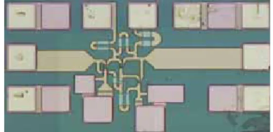
1.4µm×9µm, 1.4µm×6µm, and 1.4µm×9µm while the bias currents for the transistors are 4.8mA, 2.9mA, and 11.5mA, respectively. Thus, the total power consumption is less than 100mW. The die photograph of the finished circuit is shown in Fig. 4.
Fig. 4. Die photograph of HBT wideband amplifier HP8510 network analyzer in conjunction with the cascade probe station was used to measure the characteristics of the wideband amplifier. The simulated, measured, and predicted results are shown in Fig. 5(a), Fig. 5(b), Fig. 5(c), Fig. 5(d) and Fig. 5(e) for S21,
S11, S22, Z21(open load transimpedance) and
ZT(50Ω load transimpedance), respectively.
The measured S21 exhibited a flat response
with a 3-dB bandwidth of 11.6GHz and in-band return loss |S11| and |S22| were
smaller than –10dB. Note that at higher frequencies (>10GHz), the simulated |S21|
with TLM agreed better with the measured |S21| as compared with the simulated |S21|
without TLM. The predicted |S21| at low
frequency by the method we proposed is 17.7dB, in good agreement with the simulated |S21| 17dB and the measured |S21|
16dB. Also shown are the calculated values of frequency responses from our pole and zero theory for |S21|, |S11|, |S22|, |Z21|, and |ZT|.
Reasonably good agreement with the experimental results is found. The predicted
4 bandwidth is 11.4GHz, which is comparable to the simulated result with TLM of 11.4GHz and the measured result of 11.6GHz. Also shown in Fig. 5(d) and 5 (e) are the transimpedances calculated with an assumed photo detector capacitive load (100fF) and wire-bond interconnect inductance (1nH). Clearly, this degrades the effective transimpedance and hence its influence must be considered carefully in the circuit design. The group delay response with all these feedback loops is shown in Fig. 6 and is compared to that without peaking capacitors. As can be seen the peaking technique has a detrimental effect on group delay.
5. Conclusion
The methodology for the analysis and design of a matched-impedance wideband amplifier with multiple feedback loops was proposed. Expressions for voltage gain, current gain, loop gain, transimpedance gain, bandwidth, input/output resistance were derived. A general method for the determination of the frequency responses of input/output return losses from the poles of voltage gain was also presented. The first InGaP/GaAs HBT wideband amplifier with the Kukeilka configuration was designed by the proposed methodology. The experimental results showed that small signal gain of 16dB and a 3-dB bandwidth of 11.6GHz with in-band input/output return losses less than 10dB were obtained. The calculated values of small signal gain, bandwidth, input/output resistance and frequency responses agreed well with those from experimental results.
Fig. 5. (a)S21 (b)S11 (c)S22 (d) Z21 (e)ZT of wideband
amplifier
Fig. 6. Group delay 6. References
1. S. S. Lu etc., “A novel interpretation of transistors S-parameters by poles and zeros for RF IC circuit design,” IEEE Trans. on Microwave Theory and Techniques, Vol. 49, pp. 406-409, Feb. 2001
5 7. 主持人自評:
本計畫成果以已投稿至 IEEE Journal of Solid State Circuits,並已被接受,預計於 2002 年六 月刊登,且被Editor 評為 a good contribution to the Journal,故可謂研究成果極佳。
第二年度成果報告
中文摘要 本計畫首度以磷化銦鎵/砷化鎵異質接面 製程成功地實現 5.7GHz 單晶片內插式壓控振 盪器。不同於傳統上改變共振腔電容,本研 究以改變開路增益的方式控制頻率變化,實 驗證實在中心頻率 5.7GHz 時,頻率可調範圍 達到 400 MHz,可成功地應用於 ISM 頻段。 關鍵詞:磷化銦鎵,砷化鎵,內插式,壓控 振盪器。Abstract — A 5.7 GHz monolithic interpolative
voltage controlled oscillator using InGaP/GaAs HBT technology is demonstrated for the first time. Frequency tuning is achieved by changing the open loop gain instead of the tank capacitor. The experimental result showed that a 400-MHz tuning range at 5.7 GHz was realized, which can meet the requirement of 5.7GHz ISM band.
1. INTODUCTION
Voltage-controlled oscillators (VCO’s) are widely used in communication systems. Among the many versions of the VCO’s, such as relaxation oscillators [1], ring oscillators [2], and LC sinusoidal oscillators [3], it is generally accepted that LC sinusoidal oscillators have the best high frequency-performance in terms of phase noise characteristics and frequency stability [4]. Most LC oscillators use varactors to vary their oscillating frequencies. Nguyen and Meyer, however, proposed and realized an interpolative VCO [4] in which the oscillating frequency is interpolated from two resonant frequencies of two LC resonators and hence wide tuning range can be obtained quite easily. In their work a tuning range of 200-MHz at 1.8 GHz was obtained by using an oxide-isolated BiCMOS IC process with typical fT (n-p-n) = 10 GHz.
Recently FCC in the United States has proposed to allocate 300MHz of spectrum in 5-6GHZ band for ISM use, and the wireless LAN is one potential application which could exploit this new spectral allocation [5]. Consequently, an oscillator with a tuning range of 300-MHz at 5.7 GHz is necessary. In order to meet the requirements of high operating frequency and wide tuning range, we were motivated to use InGaP/GaAs HBT rather than BiCMOS IC process to realize the monolithic interpolative oscillators. The experimental results showed that a 400-MHz tuning range centered at 5.7 GHz , phase
noise of –96 dBc/Hz measured at 100 kHz offset from the carrier (5.7 GHz ) and output power of –13 dBm were obtained.
2. PRINCIPLES OF CIRCUITDESIGN
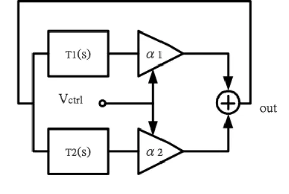
The detailed analysis of the interpolative oscillator has been done in Ref. [4]. However, a different view- point in obtaining the open loop gain the VCO is presented in this paper. The fundamental idea of the interpolative VCO according to Ref. [6] is summarized as follows. This feedback oscillatory system as shown in Fig.1 incorporates two transfer functions, T1(s) and T2(s), whose
outputs are scaled by variable factors α1 and α2,
respectively, and summed. The overall open-loop transfer function is therefore equal to L(s) = α1‧T1(s)+ α2‧T2(s),
which must be equal to +1 for the system to oscillate. In the extreme case where α1=0 or α2=0, the oscillation
frequency ωC is
Fig. 1. The block diagram of the interpolative VCO
determined by only T2(s) or T1(s) and for intermediate
values of α1 and α2, ωC can be interpolated between its
lower and upper bounds. .
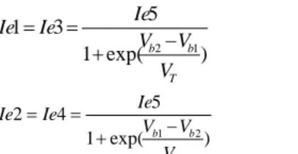
The core circuit of the interpolative VCO is depicted in Fig. 2 where all the transistors in this figure are identical. The control voltage VC is applied across the base nodes of
Q1 and Q2 (also Q2 and Q3) to modify the transconductances (gm1 and gm2) of Q1 and Q2,
respectively. Note that the collector bias current IC1 of Q1
equals that IC4 of Q4 and so does IC2 of Q2 to IC3 of Q3,
and IC5 of Q5 to IC6 of Q6. Furthermore,
IC1+IC3≅IC5≅I/2≅IC6≅IC2+IC4, where I is the constant
curren source in Fig. 2. In fact IC1, IC2, IC3, and IC4 can be
given by
T1(s) α1
T2(s) α2
Vctrl
) exp( 1 5 3 1 1 2 T b b V V V Ie Ie Ie − + = = (1) ) exp( 1 5 4 2 2 1 T b b V V V Ie Ie Ie − + = = (2) Because transconductances are proportional to the collector currents of BJT's, (1) and (2) can be rewritten as:
) exp( 1 5 3 1 1 2 T b b V V V gm gm gm − + = = (3) ) exp( 1 5 4 2 2 1 T b b V V V gm gm gm − + = = (4) where Gm = I/(2VT)=gm5=gm6.
Fig. 2. The core circuit of the VCO. This a simplified AC schematic, and the DC bias is not shown here.
The total open loop gain L(s) can be found as follows. Since the output of the VCO will be taken differentially between the base nodes of Q5 and Q6, we break the loop there and then apply a test voltage Vx. Because of the symmetry of the circuit, it can be thought of as Vx/2 is applied to the base of Q6 and –Vx/2 to the base of Q5.
Superposition can be used for the ease of analysis. That is, first the returned voltage appeared at base node of Q6 is calculated by applying Vx/2 to base of Q6 and zero voltage to the base of Q5. Then the returned voltage appeared at the base node of Q5 is calculated by applying –Vx/2 to the base node and zero voltage to the base node of Q6. The total returned voltage will be the difference of the two returned voltages in previous two cases. In the former case, the signal traverses along the path numbered from #1 to #4 (the left loop) with a returned voltage of L1(s) Vx/2 while the latter along the
path from #a to #d with returned voltage of L2(s) (-Vx/2).
L1(s) and L2(s) represent the loop gains of the left loop and the right loop, respectively. The total returned voltage is then (L1(s) + L2(s)) Vx and hence the total loop gain L(s) is L1(s) + L2(s). L1(s) and L2(s) can be shown to be
) 2 ( ) 1 ( ) exp( 1 5 ) ( 6 6 3 3 1 1 1 2 1 1 2 1 C C C C R L s Cx L s sL V V V gm s L T b b + + ⋅ + + ⋅ − + − = π (5) ) 2 ( ) 1 ( ) exp( 1 5 ) ( 5 5 4 4 2 2 2 2 2 2 1 2 C C C C R L s Cy L s sL V V V gm s L T b b + + ⋅ + + ⋅ − + − = π (6) where 6 6 3 6 6 2 1 2 ) 2 ( C C C C C C C Cx + + + ⋅ + = π π (7) 5 5 4 5 5 4 2 2 ) 2 ( C C C C C C C Cy + + + ⋅ + = π π (8)
Therefore L(s) can be written as follow
L s L s L s T s T s ( ) ( ) ( ) ( ) ( ) = + ⋅ + ⋅ 1 2 1 2 2 =α1 α (9) where ) 2 ( ) 1 ( 5 ) ( 6 6 3 3 1 1 1 2 1 1 C C C C R L s Cx L s sL gm s T + + ⋅ + + ⋅ − = π (10) Q1 Q2 Q3 Q4 Q5 Q6 C1 R1 L1 L2 R2 C2 C3 C6 C4 C5 1 2 3 4 c d a b
Fig.3. The complete circuit schematic of the monolithic VCO. ) 2 ( ) 1 ( 5 ) ( 5 5 4 4 2 2 2 2 2 2 C C C C R L s Cy L s sL gm s T + + ⋅ + + ⋅ − = π (11) ) 1 2 exp( 1 1 1 T V Vb Vb − + = α ) 2 1 exp( 1 1 2 T V Vb Vb− + = α (12)
Finally, the open-loop gain L(s) is set to unity for the system to oscillate,.
3. CIRCUIT FABRICATION& MEASURED RESULTS
The complete circuit of the interpolative VCO based on the design principles presented in section II is shown in Fig.3. A single-to-differential converting circuit consisting of Q9 and Q10 is used to convert the single-ended control voltage Vctrl to the control voltage VC. The differential
output voltage across the base nodes of Q5 and Q6 of the core circuit is converted to a single-ended output voltage Vout by a differential amplifier composed of Q12 and Q13. The simulation result of oscillation frequency versus Vctrl by Star-HSPICE is shown in Fig. 4. InGaP/GaAs HBT IC process with fT = 40 GHz is used to fabricate the VCO and the die photograph of the finished VCO is
shown in Fig. 5. The measured characteristics of oscillation frequency versus Vctrl exhibit a tuning range of 400MHz extending from 5.45GHz to 5.85GHz as shown in Fig. 4. For a Vctrl of 2.5 V, the phase noise measured at 100 kHz offset from the carrier (fo=5.7 GHz) is -96dBc/Hz. An output power level of –13dBm is also obtained. All these results are better than the previous reported values of
oscillating frequency (1.8 GHz), tuning range (200 MHz), phase noise (-88 dBc/Hz) and output power (-23 dBm). The reason is obviously due to the better technology (InGaP/GaAs) we choose. Q1 Q2 Q3 Q4 Q5 Q6 C1 R1 L1 L2 R2 C2 C3 C6 C4 C5 Q9 Q10 Q7 Q11 Q8 I bias Q12 Q13 Q14 out+ out-out+ out-Output Vctrl
Fig.4. Measurement and simulation result.
Fig.5. The die photograph of the monolithic VCO.
4. CONCLUSION
The first interpolative VCO using InGaP/GaAs HBT technology is reported. A 400-MHz tuning range at 5.7 GHz is achieved, which can meet the requirements of the recent FCC release of 300MHz spectrum in 5-6GHZ band for ISM use. The performance of the InGaP/GaAs interpolative VCO is better than that of BiCMOS VCO in terms of oscillating frequency, tuning range, phase noise and output power.
自我評估:本研就究按計畫成功地製出 5.7GHz 振盪 器 。 本 計 畫 亦 衍 生 出 一 篇 IEEE Trans. Microwave Theory and Technique, 二篇 IEEE Trans. Electron Device, IEEE Electron Device Lett., 一篇 IEE Electronics Lett., 二篇 Microwave & Optical Technology Lett.,研究成果 相當不錯。
REFERENCES
[1] J. T. Wu, “A bipolar 1-GHz multi-decade monolithic variable-frequency oscillator,” in ISSCC Dig. Tech.
Papers, Feb. 1990, pp. 106-107.
[2] K. M. Ware, H. S. Lee, and C. G. Sodini, “A 200-MHz CMOS phase-locked loop with dual phase detectors,” IEEE J. Solid-State Circuits, vol. 24, no. 6, pp. 1560-1568, Dec. 1989.
[3] B. Parzen, Design of Crystal and Other Harmonic
Oscillators, New York: Wiley, 1983.
[4] N. M. Nguyen and R. G. Meyer, “A 1.8-GHz Monolithic LC Voltage-Controlled Oscillator,” IEEE
J. Solid-State Circuits, vol. 27, no. 3, pp. 444-450,
Mar. 1992. [5] FCC
[6] B.Razavi,“RF Microelectronics”, New Jersey:Prentice Hall,1998. Tuning Range 5.3 5.4 5.5 5.6 5.7 5.8 5.9 6 2 2.2 2.4 Vctrl 2.6 2.8 3 Freq(GHz) Measured Simulated
第三年度成果報告
中文摘要 本計畫以磷化銦鎵/砷化鎵異質接面製程 成功地實現 2.4GHz 單晶片接收機。接收機電 路由一寬頻放大器、微混波器、電壓控制振 盪器、雙端轉單端轉換器和一緩衝器組成。 實驗結果顯示當本地震盪器頻率為 2.8GHz 時 功率轉換增益為 43dB;P1dB為-58dBm;線性 度 IIP3 為 -56dBm ; 直 流 功 率 消 耗 為 59.4mW。 關鍵詞:磷化銦鎵/砷化鎵異質接面、寬頻放大器、 微混波器、電壓控制振盪器、雙端轉單端轉換器。Abstract
An integrated 2.4GHz IF Receiver using InGaP/GaAs HBT technology is demonstrated. The circuit is composed of a wideband amplifier, micromixer、voltage control oscillator、output balun and buffer. The experimental results showed that power conversion gain is 43dB with the fixed LO frequency, 2.8GHz. The input referred P1dB is –58 dBm. The IIP3 of the circuit
is –56dBm. The DC power consumption is 59.4mW.
Keywords: InGaP/GaAs HBT, wideband
amplifier, micromixer, VCO, output balun.
二、計畫緣由及目的
he design goal of this project is to design an 2.4GHz receiver. The receiver is used as the IF circuit in 38GHz wireless transceiver system. The IF frequency of the receiver is 400MHz; besides, the image problem can be neglected because there are filters in front of the 2.4GHz receiver. This circuit includes the wideband amplifier, VCO with its output buffer, mixer with output active balun.
As shown in figure 1, the receiver function block gives the overview signal flow in
the receiver. In the following, we will present the topology and measurement results of each component in the 2.4GHz receiver.
Figure 1. Function block of InGaP/GaAs HBT 2.4GHz receiver
三、研究方法
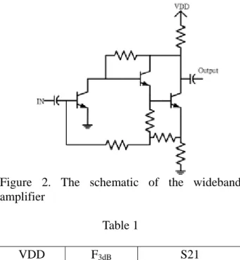
The schematic of the wideband amplifier used in the 2.4GHz receiver is shown in figure 2. It is basically a two stage dual feedback circuit. We use two feedback resistors to increase bandwidth and gain. The second stage uses Darlinton pair to increase bandwidth and gain. The simulation result of wideband amplifier is summarized in table 1.
Figure 2. The schematic of the wideband amplifier
Table 1
VDD F3dB S21
5 Volt 8GHz 30dB
S11 S22 Power consumption
<-10dB <-10dB 31.7mW
Figure 3 includes mixer, IF filter, active balun, and output buffer. The schematic of mixer is shown in figure 4. Barrie Gilbert proposed micromixer in 1977 [1]. It is suitable for wide band operation for its wide band input impedance matching characteristic. The input transconductance stage of typical Gilbert cell is modified into a single-to-differential class AB transconverter. The bipolar junction transistor (BJT) differential pair widely used as the RF input stage is replaced by a bisymmetric Class-AB topology based on translinear principles. Because the single ended RF port of the micromixer is wideband matched to 50 ohm, it can be directly connected to the wideband amplifier output port. The LO buffer drive the double balanced current switches differentially with large signals. Besides, current injection [2] technique is applied to enhance the conversion gain of the mixer. A diode-connected circuit is added as another current source.
After the micromixer, the modified push-pull balun is used to convert differential mixer output into single ended. Figure 4 is a push-pull type balun, which is composed of a common-emitter with degenerative resistor and the common-collector stage. The degenerative resistor R12 controls the gain of the common
emitter path for the same amount of gain for both inverting and non-inverting signals, resulting in maximum cancellation of LO leakage at the output of the balun. R11 is
included for output impedance matching. The common-collector path provides highly linear performance and the common-emitter is more linear than differential-pair for the same bias current and transconductance [3]. So the push-pull type balun provides good linearity. Because the differential output signal has better LO leakage suppression and single ended output is
feasible for measurement, the active balun is used in this design. The IF low-pass filter at mixer load is consists of capacitors paralleled with resistors. Finally, the output buffer is designed for matching the output impedance of spectrum analyzer.
Figure 3. Schematic of mixer and IF amplifier in the 2.4GHz receiver.
Figure 4. Push-pull type balun
Figure 5 is the schematic of the voltage control oscillator in the InGaP/GaAs HBT 2.4GHz receiver. It is a cross-coupled topology. Two capacitors are inserted between base and collector of two transistors. They can prevent transistors into saturation to increase output voltage amplitude. The LO buffer separates the
oscillator and mixer, providing proper amplitude level to the LO port of mixer. The LO buffer is consist of common emitter and small capacitor as DC block not to affect the oscillation frequency of VCO. The simulation result of the VCO and the buffer is summarized in table 2.
Figure 5 Voltage control oscillator in the InGaP/GaAs HBT 2.4GHz receiver Table 2 V D D Power consumpti on Frequency Output Voltage Amplitude Tune Voltage 5 v 9mW 2.7~3.2GHz 0.25Vpp 0~5V
四、結論與成果
Figure 6 is the die photo of the InGaP/GaAs HBT 2.4GHz receiver. The on-wafer measurement setup is shown in figure 7. Instruments for the measurement are signal generators and spectrum analyzer. From the leakage LO signal at mixer output, the VCO frequency can be known. In the measurement, we found that the LO frequency is shifted from designed 2.7~3.2GHz to 2.73~2.84GHz. Although the LO is shifted, the receiver can still work normally. Therefore we set input RF frequency equal to 2.4GHz and LO frequency is 2.8GHz in the measurement. Therefore the output IF frequency is 400MHz.
Figure 6 The die photo of the InGaP/GaAs HBT 2.4GHz receiver.
Figure 7 On-wafer measurement setup.
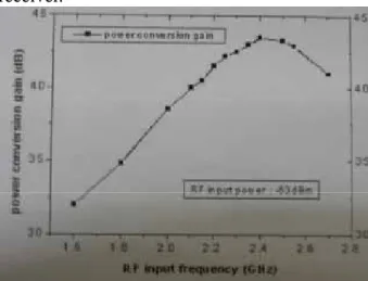
Figure 8 shows the power conversion gain as function of the RF input power in the InGaP/GaAs HBT 2.4GHz receiver. The power conversion gain is 43dB, almost the same with the simulation. The input referred P1dB is –
58dBm. And the IIP3 of the circuit is –56 dBm shown in figure 9. Figure 10 shows the output power conversion gain as the function of RF input frequency at fixed LO frequency, 2.8GHz.
Figure 8 The power conversion gain as function of the RF input power in the InGaP/GaAs HBT 2.4GHz receiver.
Figure 9 Third order Inter-modulation characteristics of the InGaP/GaAs HBT 2.4GHz receiver.
Figure 10 The output power conversion
gain as the function of RF input frequency at fixed LO frequency, 2.8GHz.
自我評估:本研究按計畫成功地製出 2.4GHz 接收 機。本計畫亦衍生出一篇 IEEE Microwave and wireless components letter (Oct.,2004),研究成果相當不錯。
五、參考文獻
[1] Barrie Gilbert, “the micromixer: a highly linear variant of the gilgert mixer using a bisymmetric class-AB input stage,” IEEE
Journal of Solid State Circuits, VOL.32
NO.9 SEPTEMBER 1997.
[2] Manku, T., “A charge-injection method for Gilbert cell biasing,” NacEachern, L.A; Electrical and Computer Engineering, IEEE
Canadian Conference, VOL.1, pp.365-368,
1998.
[3] Keng Leng Fong and Robert G.Meyer, “High-Frequency Nonlinearity Analysis of Common-Emitter and Differential-pair Transconductance Stages,” IEEE Journal of
Solid State Circuits, VOL.33, pp.548-555,