Hydrogen etch of GaN and its application to produce porous GaN
caves
Yen-Hsien Yeh*, Ying-Chia Hsu, Yin-Hao Wu, Kuei-Ming Chen and Wei-I Lee
Dept. of Electrophysics, National Chiao Tung Univ./ No.1001, Daxue Rd., East Dist., Hsinchu City
300, Taiwan (R.O.C.)
ABSTRACT
Although it is known that GaN tend to decompose in hydrogen environments, there has been few investigations in hydrogen etch of GaN. This study performs a systematic research on hydrogen etch of GaN under various pressures. It is observed that hydrogen atoms initially etch into GaN to form pinholes. Dislocations are usually the preferred places for initial hydrogen etch, but not all etched holes result from dislocations. When etched at low pressure and high temperature, deep vertical holes extending several microns can be formed by the hydrogen etch. However, when etch is performed at high pressure, apparent lateral etch are observed under the initial holes, leading to bollard-like GaN posts. From this systematic study, a model has been proposed to explain the vertical and the lateral etching mechanisms. With the established model, a sequential etch of GaN in hydrogen under varying pressure has been designed to successfully maintain a smooth GaN front surface, but to etch the underlying GaN to form a porous cave structure. Thick GaN films are then overgrown on such GaN layers with the hydride vapor phase epitaxy technology. It is demonstrated that the overgrown GaN thick films can self-separate from the underlying Al2O3 substrates.
Keywords: Hydrogen etch, Hydride vapor phase epitaxy, Gallium Nitride, Semiconducting III-V materials
1. INTRODUCTION
Recently, GaN becomes a major wide band gap semiconductor for fabricating green to ultraviolet optoelectronic devices. Various processes have been developed for studying the properties of GaN or making devices. Among these techniques, etching is one of the most important steps. For example, etching process is necessary for making patterned structure on the surface of GaN in order to reduce stress and dislocation density during manufacturing devices or large-area
free-standing GaN substrates.1-5 Unfortunately, conventional wet etching is difficult to etch GaN due to its high chemical
stability. The effective methods are dry etching techniques such as reactive ion etching (RIE)6,7 and inductively coupled plasma (ICP).8,9 The feature of these dry etching processes is anisotropic etching; GaN is etched in the vertical direction. However, the obtainable patterned structures are limited to the single direction etching. It is valuable to develop an etching technique which has both vertical and lateral etching direction. Additionally, an in situ maskless etching can also help to simplify the manufacturing processes of GaN substrate and device.
This work investigates the morphology of GaN etched in hydrogen (H2) at high temperature. Previous literatures have studied GaN decomposition in H2 for understanding the influence of H2 during GaN growth;10-12 therefore the surface morphology is not investigated in detail. In order to examine the morphology, GaN has been etched in this study, and then several profiles show the potential of H2 etch for pattern producing. A model has been developed to explain the mechanisms of H2 etch. Finally, a patterned structure with vertical and lateral etching profile has been made, and the following overgrowth experiment illustrates the applicability of H2 etch.
2. EXPERIMENT
Samples used in the following experiments were MOCVD-grown GaN templates. They were cleaned by ultrasonic cleaner for removing contamination before each experiment. After experiment, the surface morphologies were observed through high-resolution field emission scanning electron microscope (FE-SEM, Hitachi s-4700i).
2.1 Hydrogen etch under various pressures
The system used in the experiments was a home-made horizontal HVPE reactor. Samples were heated to 1050˚C under a constant pressure. In addition to nitrogen (N2), ammonia (NH3) was introduced into the reactor to avoid GaN
decomposition during heating. After the temperature reached 1050˚C, NH3 was shut off and H2 was introduced to begin etching, the flow rate of H2 was 1 slm. Seven samples labeled A, B, C, D, E, F and G were etched under pressures of 700, 600, 500, 400, 300, 200 and 100 Torr, respectively. Each sample was etched for 10min and examined by SEM.
2.2 Etch pit density (EPD) experiment
There are two EPD experiments in our study; one of them was performed to verify the etching mechanisms, and the other was performed to determine the dislocation density. In these experiments, samples were immersed in the solution of H3PO4 and H2SO4 at 220˚C for 20min. The resulting surfaces were examined by SEM and AFM.
Sequential etch was performed using a pressure variation. Following the same procedure as described in section 2.1 but with additional etching step, the sample first etched in H2 under a low pressure of 100 Torr for 20min, and then under a high pressure of 700 Torr for 10min. There were two samples performed sequential etch, and one of them was subjected to the following overgrowth process. In the overgrowth process, the sample which was performed sequential etch was grown at 1050˚C under a pressure of 700 Torr for 120min, and the V/III ratio was 40.
3. RESULTS AND DISCUSSION
3.1 Hydrogen etch under various pressures
Figure 1 shows the plan views, tilted views and cross-section views of the seven samples etched at different pressures. It can be noticed that the etching profiles markedly vary with pressures. These profiles can be classified into three types according to their shapes, as shown in Fig. 2. At high pressure (~700 Torr), the etching depth is 200~300nm, and the profile resembles Fig. 2(a). At intermediate pressure (~400 Torr), however, the surface becomes relatively flat and a few deep holes appeared, as shown in Fig. 2(b). At low pressure (< 200 Torr), the surface becomes more flat and a lot of deep holes appeared, as shown in Fig. 2(c).
3.2 The model of hydrogen etch mechanisms
Based on the experimental results, we have developed a model attempting to explain the evolution of the surface
morphology. It is proposed from the previous studies that H2 enhances GaN decomposition.10 H and N atoms combine to form NH3 at high temperature, and then liquid Ga is subsequently left on the surface.10,13,14 Ga droplet, which remains as long as the Ga desorption rate is not high, has been observed in our low temperature experiment. At high temperature, however, Ga desorption rate is high enough to avoid Ga droplet production.10,14 On account of the H mostly reacting with N, we presume that the facet formed with N atoms (N-polarity) will be unstable during H2 etch while the facet formed with more proportion of Ga atom will be more stable. The as-grown surface of a MOCVD-grown c-plane GaN film is Ga-polarity (Ga-face), and the reverse side is N-polarity (N-face). The inclined {10-11}, {11-22} facets are mainly N-polarity; however, nonpolar (a-plane & m-plane) facets contain equal numbers of Ga and N atoms. Therefore, we suppose that during H2 etch, the relative stabilities of facets follow the order: Ga-face > nonpolar face > inclined face > N-face. The formation of the profile in Fig. 2(a) can be explained by using the concept above, and as shown in Fig. 3. As H2 arriving at surface it is difficult for H2 to decompose most of GaN on the surface because of the high stability of Ga-face; therefore, etching in the vertical direction occurs at the weak areas such as dislocation sites, as shown in Fig.
3(b) (the dotted lines indicates the dislocations). Nitrogen is produced during etching and makes the nonpolar sidewall unstable;3,4 as a result, the lateral etching begins at the bottom of the holes, as shown in Fig. 3(c). When the sidewall is etched for some distance, N-face facet is exposed and then etched due to its instability; therefore the etching begins in the upward direction, as shown in Fig. 3(d). The resulting etching profile is shown in Fig. 3(e). A lot of holes with this etching profile expand and merge due to the high etching rate at high pressure, and then make the morphology resemble a surface decorated with bollards or mooring posts, as shown in Fig. 2(a). On the other hand, the etching rate is lower at intermediate pressure; therefore nitrogen is produced slightly and dissipates rapidly. Nonpolar facets become stable, and then some deep holes appear, as shown in Fig. 2(b). The etching rate is lowest at low pressure, so nitrogen is produced more slightly and dissipates more rapidly. Nonpolar facets become more stable, and a lot of deep holes appear, as shown in Fig. 2(c). It is suggested that the vertical etching direction is dominant at low pressure.
FIG. 1. SEM images of the samples etched at different pressures in plan views, tilted views and cross-section views: (a) 700, (b) 600, (c) 500, (d) 400, (e) 300, (f) 200, and (g) 100 Torr. All the scale bars are 1μm.
FIG. 2. Three types of profiles: (a) bollards or mooring posts, (b) a few deep holes, and (c) a lot of deep holes.
FIG. 3. The stages of H2 etch at high pressure: (a) unetched template, the top surface is Ga-face and the dotted line indicates the dislocation, (b) H2 etch at the dislocation site, (c) lateral etching at the bottom of the hole, and then N-face facet is exposed, (d) etching in the upward direction due to the instability of N-face, and (e) the resulting etching profile.
3.3 Etch pit density (EPD) experiment
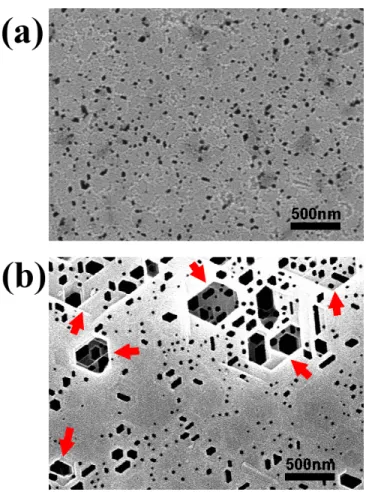
To determine the etching occurring at the weak areas such as dislocation sites, a piece of sample cut from sample G has been performed EPD experiment. Fig. 4(a) shows the surface of original sample without performing EPD experiment, and Fig. 4(b) shows the surface of sample performed EPD experiment. It can be found that some tops of the holes expand, even cross over the adjacent holes, as indicated by the arrows; however, there are also holes which do not change their size of the top. It can also be found that there are no hexagonal V-shape pits on the surface of sample performed EPD experiment. Normally, the V-shape pits form at dislocation sites on the surface after EPD experiment; hence we deduce that the absence of V-shape pits comes from all dislocations are etched to form holes. The density of the holes shown in Fig. 4(a) is estimated about 7×109cm-2, yet the dislocation density of the template used in this experiment is about 5×108cm-2. Therefore, we deduce that most holes are not resulted from the etched dislocations; they are probably the ones who do not change their size after EPD experiment in Fig. 4(b). We conclude that all dislocations are etched to form holes, but not all the holes are resulted from the etched dislocations. The formation of the holes which are not resulted from the etched dislocations is under study.
FIG. 4. SEM images of (a) the original sample without performing EPD experiment, and (b) the surface of sample performed EPD experiment. The arrows indicate some of the expanded tops of the holes.
3.4 Sequential etch and overgrowth experiment
According to the developed model, we expect that it would produce various morphologies with a pressure variation etching process. Fig.5 shows the sample etched by Sequential etch method. We deduce that the structure is formed as the following procedure: in the first step, many deep holes produce on the surface at low pressure; in the second step, H2 continues to etch the bottom of the holes at high pressure due to the weakness of these regions. A lot of nitrogen atoms are produced around the bottom of the holes, and then the sidewalls (nonpolar facets) become unstable due to the nitrogen atoms. Consequently, lateral etching accompanied with the upward direction begins, and then it expands the bottom of the holes. As a result, the final profile is shown in Fig. 5, and it has a flat surface but porous inside.
FIG. 5. SEM image of the sample etched by two-step process. The sample has porous GaN caves, and the top surface is smooth.
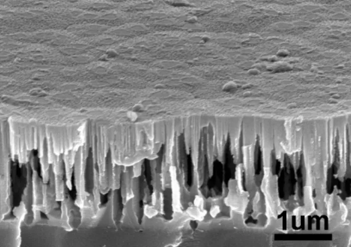
The overgrown sample has self-separated from the underlying sapphire substrate, as shown in Fig. 6. It is suggested that the porous caves make the interface of GaN and sapphire become weak, so the thick film separate from substrate due to the stress which rise during cooling. This experiment demonstrates one possible application of H2 etch, and we believe that H2 etch is also helpful for the reduction of threading dislocation density during the overgrowth process. But the dislocation density of the self-separated sample does not reduce hugely; Fig. 7 shows the AFM image of the surface of self-separated sample performed EDP experiment. The dislocation density is estimated about 2×107cm-2, and this value is just a little lower than that of the thick film which is grown without H2 etch. We consider that the growth condition needs to be optimized in order to reduce the dislocation density.
FIG. 6. GaN thick film self-separated from sapphire; the thickness is about 300μm
Fig. 7. AFM image of the surface of self-separated sample performed EDP experiment. The dislocation density is estimated about 2×107cm-2.
4. SUMMARY
In conclusion, different morphologies appear on the GaN surfaces etched in H2 under different pressures at 1050˚C. It is presumed that etching begins in certain weak areas such as dislocation sites. In addition to vertical direction, H2 etch also has lateral and upward direction at high pressure. By combining the high etching rate at high pressure, the holes expand and merge, and they make the surface profile resemble clustered bollards or mooring posts. On the other hand, H2 etch
merely has vertical direction at low pressure, and that makes the surface be decorated with holes. EPD experiment shows all dislocations have been etched to form holes at low pressure, but not all the holes are resulted from etched dislocations. Sequential etch which uses a pressure variation produces porous GaN caves with a flat top surface. The thick film
overgrown on the patterned surface has self-separated from the underlying substrate; hence it demonstrates the applications of H2 etch.
REFERENCES
[1] O.H. Nam, M.D. Bremser, T.S. Zheleva, and R.F. Davis, “Lateral epitaxy of low defect density GaN layers via organometallic vapor phase epitaxy,” Appl. Phys. Lett. 71, 2638 (1997).
[2] A.Sakai, H. Sunakawa, and A. Usui, “Defect structure in selectively grown GaN films with low threading dislocation density,”, Appl. Phys. Lett. 71, 2259 (1997).
[3] K. Hiramatsu, K. Nishiyama, A. Motogaito, H. Miyake, Y. Iyechika, and T. Maeda, “Recent Progress in Selective Area Growth and Epitaxial Lateral Overgrowth of III-Nitrides: Effects of Reactor Pressure in MOVPE Growth,” Phys. Stat. Sol. (a) 176, 535 (1999).
[4] K. Hiramatsu, K. Nishiyama, M. Onishi, H. Mizutani, M. Narukawa, A. Motogaito, H. Miyake, Y. Iyechika, and T. Maeda, “Fabrication and characterization of low defect density GaN using facet-controlled epitaxial lateral overgrowth (FACELO),” J. Cryst. Growth 221, 316 (2000).
[5] I. Kidoguchi, A. Ishibashi, G. Sugahara, and Y. Ban, “Air-bridged lateral epitaxial overgrowth of GaN thin films,” Appl. Phys. Lett. 76, 3768 (2000).
[6] Adesida I, Mahajan A, Andideh E, Khan MA, Olsen DT, and Kuznia JN, ”Reactive ion etching of gallium nitride in silicon tetrachloride plasmasa,” Appl. Phys. Lett. 63, 2777 (1993).
[7] M.E. Lin, Z.F. Fan, Z.Ma, L.H. Allen, and H. Morkoç, “Reactive ion etching of GaN using BCl3,” Appl. Phys. Lett. 64, 887 (1994).
[8] R.J. Shul, G.B. McClellan, S.A. Casalnuovo, D.J. Rieger, S.J. Pearton, C. Constantine, and C. Barratt, “Inductively coupled plasma etching of GaN,” Appl. Phys. Lett. 69, 1119 (1996).
[9] Smith SA, Wolden CA, Bremser MD, Hanser AD, Davis RF, and Lampert WV, “High rate and selective etching of GaN, AlGaN, and AlN using an inductively coupled plasma,” Appl. Phys. Lett. 71, 3631 (1997).
[10] D.D. Koleske, A.E. Wickenden, R.L. Henry, J.C. Culbertson, and M.E. Twigg, “GaN decomposition in H2 and N2 at MOVPE temperatures and pressures,” J. Cryst. Growth 223, 466 (2001).
[11] Z.J. Reitmeier, J.-S. Park, W.J. Mecouch, and R.F. Davis, “In situ cleaning of GaN(0001) surfaces in a metalorganic vapor phase epitaxy environment,” J. Vac. Sci. Technol. A 22, 1975 (2004).
[12] M.A. Mastro, O.M. Kryliouk, M.D. Reed, T.J. Anderson, and A.J. Shapiro, “Thermal Stability of MOCVD and HVPE GaN Layers in H2, HCl, NH3 and N2,” Phys. Stat. Sol. (a) 188 (1), 467 (2001).
[13] N. Kobayahi and Y. Kobayahi, “In-situ optical monitoring of surface morphology and stoichiometry during GaN metal organic vapor phase epitaxy,” Appl. Surf. Sci. 159/160, 398 (2000).
[14] T.H. Myers, B.L. VanMil, J.J. Holbert, C.Y. Peng, C.D. Stinespring, J. Alam, J.A. Freitas Jr., V.A. Dmitriev, A. Pechnikov, Y. Shapovalova, and V. Ivantsov, “Use of high temperature hydrogen annealing to remove sub-surface damage in bulk GaN,” J. Cryst. Growth 246, 244 (2002).