An Empirical Defect-Related Photo Leakage Current
Model for LTPS TFTs Based on the Unit Lux Current
Ya-Hsiang Tai, Member, IEEE, Yan-Fu Kuo, and Guo-Pei Sun
Abstract—In this paper, the photosensitive effect of n-type
low-temperature polycrystalline silicon (LTPS) thin-film transis-tors (TFTs) after dc stress is analyzed. It is found that the illu-mination behaviors for poly-Si TFTs are dependent on the defect types created by different stress conditions of hot-carrier and self-heating effects. For a given stress-induced device degradation, the anomalous illumination behaviors are observed, and these pho-to-induced leakage currents are not included in the present SPICE device model. Therefore, based on trap-assisted and Poole–Frenkel effect, an empirical defect-related photo leakage current model based on Unit Lux Current (ULC) is proposed to depict the photo-induced current after device degradation. Furthermore, the verified equation of ULC is analytically derived and has good agreement with the experimental data.
Index Terms—DC stress, leakage current, photosensitivity,
poly-Si thin-film transistor (TFT).
I. INTRODUCTION
L
OW-TEMPERATURE polycrystalline silicon (LTPS) thin-film transistors (TFTs) have attracted much attention for active matrix liquid crystal display (LCD) and active matrix organic light-emitting diode applications due to the high mo-bility and the capamo-bility of realizing integrated circuits on the same glass [1]. For its application, several ambient light sensors using poly-Si TFTs, which is one of the value-added functions for high-end flat-panel display, have been reported [2]–[7]. Photosensitivity is a significant design consideration for achiev-ing high-image-quality LCDs. However, it was reported that poly-Si TFTs suffer from several degradation mechanisms, such as hot carrier and self-heating effects [8]. The hot carrier effect has found that the degradation is related to the increase of strain bond tail states in the band gap of the poly-Si film and damaged region is near the drain. The self heating effect is reported in interface states near the source region, and the deep states in the poly-Si film near drain can be created [9]. Due to such degradation, the photo-induced leakage current is stronglyManuscript received October 15, 2009; revised February 5, 2010. Current version published April 21, 2010. This work was supported in part by the National Science Council, Republic of China, under Grant NSC97-2218-E-009-005 and in part by the MOE ATE program and MOEA Technology Development Academia under Project 96-EC-17-A-07-S1-046. The review of this paper was arranged by Editor H.-S. Tae.
Y.-H. Tai and G.-P. Sun are with the Department of Photonics and Display Institute, National Chiao Tung University, Hsinchu 30010, Taiwan (e-mail: yhtai@mail.nctu.edu.tw).
Y.-F. Kuo is with the Department of Photonics and the Institute of Electro-Optical Engineering, National Chiao Tung University, Hsinchu 30010, Taiwan. Color versions of one or more of the figures in this paper are available online at http://ieeexplore.ieee.org.
Digital Object Identifier 10.1109/TED.2010.2044292
influenced, which is difficultly designed for sensing circuits. In this paper, we deliberately apply both stress conditions to ma-nipulate the defect-related photo behaviors and modify the Unit Lux Current (ULC) [10] equations in TFTs. Comparatively, this paper focused on how additional nonuniform defects and the photo leakage mechanism influence both lateral and gate–drain overlap depletions.
II. EXPERIMENTS
The self-aligned structure of top-gate n-type LTPS TFTs with lightly doped drain (LDD) structure was used in the experiment. First, the buffer oxide and a-Si:H films were deposited on glass substrates with plasma-enhanced chemical vapor depo-sition (PECVD). The samples were then put in the oven for dehydrogenation. Then, the XeCl excimer laser scanned the a-Si:H film to recrystallize the a-Si:H film to poly-Si. After the poly-Si active area definition, 65 nm SiO2 was deposited
with PECVD as the gate insulator. Next, the metal gate was formed by sputter and then defined. The LDD and the n+
source/drain doping were formed by PH3 implantation with
dosages of 2× 1013 cm−2 and 2× 1015 cm−2, respectively. The LDD implantation was self-aligned, and the n+ regions
were defined with a separate mask. Then, the interlayer of SiNxwas deposited. Subsequently, rapid thermal annealing was
conducted to activate the dopants, whereas the poly-Si film was simultaneously hydrogenated for 30 min. Finally, contact hole formation and metallization were performed to complete the fabrication work. In this paper, n-channel LTPS TFTs having a channel width of 20 μm and a channel length of 5 μm with an LDD structure of length 2.5 μm are measured under different illumination conditions. The light was collimated and focused onto the device with top face white light illumination. The photo leakage current was induced by a halogen lamp irradiation stream with several neutral density filters (the light intensity ranging from dark to 31320 lx) through the objective of a microscope, and the light intensity was measured by a digital luminous flux meter.
Fig. 1 shows the photo leakage current, the power variation spectrum of the light source in the range of 350–750 nm, and the cross-sectional view of n-channel LTPS TFTs. In this paper, the TFTs are measured under different illumination conditions before and after bias stress. One of the stress conditions is that the drain voltage is equal to 20 V and the gate voltage is 3 V, which correspond to the hot carrier effect. The other condition of self heating stress is set to be 15 V for both the gate-to-source voltage Vgs and the drain-to-source voltage Vds.
1016 IEEE TRANSACTIONS ON ELECTRON DEVICES, VOL. 57, NO. 5, MAY 2010
Fig. 1. Cross-sectional views of n-channel LTPS TFTs with LDD structure and photo leakage current: power variation spectrum of the light source.
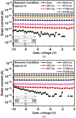
Fig. 2. Ids–Vgs transfer characteristics under different illumination condi-tions for (a) conventional LDD and (b) only one-side LDD device structures.
III. RESULTS ANDDISCUSSION
A. Photosensitivity Confirmation
The previous study [12] revealed that the photo-induced current only happens at the drain side. To further confirm that the photo sensing area is mainly at the drain electrode side and the photo-induced current is not mutually affected by the source electrodes, a conventional LDD structure and a one-side LDD structure of TFTs are designed for examination. Fig. 2(a) and (b) shows the Ids–Vgs characteristics with negative gate bias under different illumination conditions for the conventional LDD device structure and the one-side LDD device structure.
It can be seen that the off current of these two types of TFTs is lifted up to similar levels under different illumination intensities. It also reveals that the poly-Si TFT leakage current occurs at the depletion region of the drain junction and is not influenced by the source region. Therefore, the following discussion on the photosensitivity mechanism will only focus on the drain region.
B. Model Description and Analysis
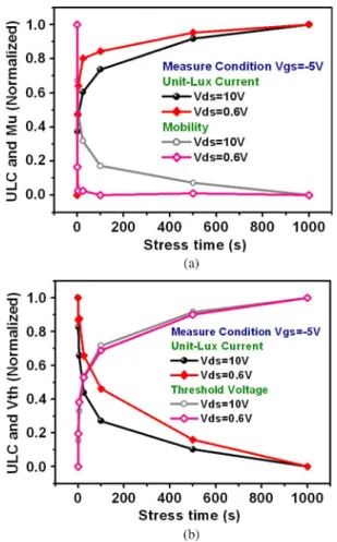
In this paper, we take into account the photo leakage current induced per unit photo flux (ULC) [10] to analyze the photo-sensitivity of the LTPS TFTs. The ULC can be expressed by a linear combination of two components: 1) the leakage current induced in the lateral depletion region and 2) the leakage current induced in the gate–drain overlap depletion region [11]. When the device is operating at the low drain voltage, the ULC is attributed to the lateral depletion region by the channel–drain junction in reverse bias. When the drain voltage is large enough, the ULC increase considered that the reverse lateral depletion at the drain region extends as the gate–drain overlap depletion junction. However, the photosensitivity of the LTPS TFTs is influenced by both the defect state distribution and the density in the drain depletion region. Thus, in the aspect of poly-Si TFTs under electrical stress, the additional defects created a close drain depletion region, and consequently the ULC is drastically varied after hot carrier and self-heating degradation. Fig. 3(a) and (b) shows the Ids–Vgs transfer characteris-tics with 1-V drain voltage before and after hot carrier and self-heating stress under different illumination conditions. The previous study [12] revealed that the photo-induced current tendency is oppositely changed by the different stress con-ditions in the lateral depletion region by the channel–drain junction in reverse bias. It increases in the case of hot carrier, whereas it decreases for self-heating. Meanwhile, it correlated photosensitivity with the device parameters, such as mobility or threshold voltage, on the LTPS TFTs. Fig. 4(a) shows a normal-ized ULC and mobility at Vds = 0.6 and 10 V, in accordance with the stress time for hot carrier stress. The variation trends have been normalized, and then we can pay attention on the tendencies of these unit parameters. As shown in the figure, it reveals that most of the trap states generated by hot carrier stress are crowded near the drain junction side. In contrast, the normalized ULC and the threshold voltage at Vds = 0.6 and 10 V, in accordance with the stress time for self-heating stress, are compared in Fig. 4(b). It demonstrates that the extra defect states created by self-heating stress are spread in the whole poly-Si thin film throughout the channel. From those previously mentioned, the nonuniform defect distributions after dc stress cause the previous ULC equations to not agree with the experiment data very well. Therefore, the following discussion will focus on accurately modifying the ULC equations for not only lateral depletion but also gate–drain overlap depletion.
C. Empirical Defect-Related ULC Model
Several mechanisms of leakage current were discussed in the previous report [13]–[16]. For the purpose of effective medium modeling characteristics, we consider the poly-Si to be a
Fig. 3. Ids–Vgs transfer characteristics with 1-V drain voltage before and after (a) hot carrier stress and (b) self-heating stress under different illumination conditions.
material with uniformly distributed trap density [10]. Due to the photocurrent behaviors of LTPS TFTs concerning the different types of additional nonuniform defects generated from various stress conditions, we suggest an empirical defect-related ULC model to describe the photosensitivity of the LTPS TFT after device degradation.
To explicitly analyze the trap-assisted leakage mechanism, an index Vdx is used to further divide the ULC into ULC1
and ULC2to individually describe the influence of lateral and
vertical field effects. At low drain bias, since the lateral electric field is relatively small, it considered that the photo-induced current is a thermally generated current dominantly. It advices us to adjust the drain-bias dependence of the ULC model to approximately exponential forms. At higher drain bias, it considered that the reverse lateral depletion at the drain region extends the vertical field effect and causes gate-induced drain leakage (GIDL) in the gate–drain overlap depletion junction. The value of the photo current should be associated with the carrier generation in the space charge region. By the junction reverse saturation current and the GIDL, the ULC2 owing to
the GIDL effect is also in an exponential relation base on the conductivity limited by the grain boundaries of the semiempiri-cal analytisemiempiri-cal model. Thus, the ULC can be modified by a linear combination of these two components as
ULC = ULC1+ ULC2 (2)
ULC1= A1· {exp [B1(Vd− Vdx)] − 1} + χ (3)
ULC2= A2· exp(−η · Vg) · {exp [B2(Vd− Vdx)] − 1} (4)
Fig. 4. (a) Normalized ULC and mobility at Vds = 0.6 and 10 V with hot carrier stress times. (b) Normalized ULC and threshold voltage at Vds = 0.6 and 10 V with self-heating stress times.
where Vdx is an indication boundary drain voltage that demar-cated the lateral depletion region and the gate–drain overlap depletion region. (We can subtract ULC1 from the total ULC
curve; the rest of the total ULC is the second component called ULC2. The drain bias that increases the ULC from zero to
positive point is an indication boundary.) χ corresponds to the photo leakage current induced by the per unit photo flux at Vdx (it is about 6.3–6.46 V before stress). A1, A2, B1, B2, and η
are all fitting parameters. A1and A2correspond to the
defect-related coefficients of ULC1 and ULC2, respectively. B1 and
B2 are the drain voltage dependences from dc stress per unit
of depletion area. η is the scaling factor of ULC2 about the
exponential dependence on the negative gate bias of ULC2.
D. Hot Carrier Effects on ULC
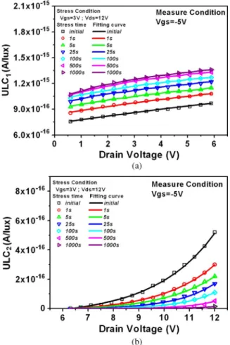
The stress conditions are that the drain voltage is equal to 12 V and the gate voltage is 3 V, which is measured at different stress times of 1, 5, 25, 100, 500, and 1000 s, to investigate the hot carrier effect on the ULC. The ULC at Vgs =−5 V with different stress times is shown in Fig. 5. Similarly, for analyzing the photosensitivity on the defects influenced by lateral and vertical field effects, we also divide the ULC measurement data into two components. It can be seen that the ULC in-crease and slightly distort at lower drain bias with stress times. However, when the device operates at higher drain bias, the
1018 IEEE TRANSACTIONS ON ELECTRON DEVICES, VOL. 57, NO. 5, MAY 2010
Fig. 5. Drain bias effect on ULC with different hot carrier stress times.
Fig. 6. (a) First component (ULC1) and (b) second component (ULC2) of
ULC versus drain bias with different hot carrier stress times.
photo-induced current is severely decreased. The calculated and experimental data of drain bias effect on the ULC with different hot carrier stress times are individually shown in Fig. 6(a) and (b). It is observed that the calculated results agree with our experiment data very well. Fig. 7(a) and (b) shows the fitting factors A1, A2 and B1, B2 of the modified ULC1 and ULC2
equations in (3) and (4) at Vgs =−5 V after hot carrier stress. It is noticed that the drain voltage dependences per unit depletion area B1and B2are raised with stress times. The tendencies of
the defect-related coefficients A1 and A2 of ULC1and ULC2
are reduced with stress times. It may be attributed to the photo
Fig. 7. Dependence of fitting factors A1, A2and B1, B2on hot carrier stress.
Fig. 8. Drain bias effect on ULC with different self-heating stress times. reexcited carrier increase, and the carriers slowly traveling by trap hopping.
E. Self Heating Effects on ULC
The stress condition is that the drain voltage is set to be 15 V for both Vgs and Vds, which is measured at different stress times of 1, 5, 25, 100, 500, and 1000 s, to investigate the self heating effect on the ULC. The ULC at Vgs =−5 V with different stress times is shown in Fig. 8. By dividing the ULC measurement data into two components, it is obvious that
Fig. 9. (a) First component (ULC1) and (b) second component (ULC2) of
ULC versus drain bias with different self-heating stress times.
the ULC decreases under lower drain voltage and is almost the same at higher drain bias with various stress times. In view of such conditions, Fig. 9(a) and (b) shows the calculated and experimental data of drain bias effect on the ULC with different self-heating stress times. Similarly, Fig. 10(a) and (b) shows the fitting factors of the modified ULC1and ULC2equations in
(3) and (4) at Vgs =−5 V after self-heating stress. It appears that B1 and B2 and A1 and A2 are nearly unchanged with
various stress times. Although hot carrier and self-heating stress affect the device photosensitivity in slightly different ways, the verified ULC equations are still properly consistent with the illumination behaviors after self-heating stress.
F. Mechanism of ULC
According to the experimental results of two stress condi-tions, a more complete mechanism of defect-related ULC is proposed to explain the photosensitive effect on the leakage current of LTPS TFT after dc stress.
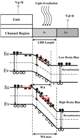
Fig. 11 illustrates the band diagrams of the unstressed de-vices under the condition of Vg < 0 along the channel direction near the drain region at low and high drain biases. Wd indicates the length of the depletion region at the drain electrode side, where electron–hole pairs can be generated under illumination in the poly-Si film. It consists of the LDD region and the high hole concentration region in the channel induced by the
Fig. 10. Dependence of fitting factors A1, A2 and B1, B2on self-heating
stress.
negative gate bias. The generated electrons move along the drain electrode and the holes flow toward channel direction. For the case of devices at low drain bias with light irradiation, when the gate bias is changed, the channel/LDD junction is similar to the abrupt p+n− junction. As the lateral depletion region increases with the drain bias, the ULC1of the conduction
mechanism in the low drain field is the thermal emission [17]. On the other hand, for high drain bias with light irradiation, the gate–drain overlap depletion region increases with both drain and gate bias, and the ULC2of the conduction mechanism at the
high drain voltage is the field-enhanced emission in the space charge region [18].
Fig. 12 shows the band diagrams of the devices after hot carrier stress under the condition of Vg < 0 along the channel direction near the drain region at low and high drain biases. When the LTPS TFT devices after hot carrier stress are under optical illumination, the numerous electron–hole pairs from the additionally created shallow tail states are generated in the lateral depletion region. Therefore, the photo leakage current obviously increases due to the photo-induced carriers from the extra states created. Fig. 13 shows the photo leakage current spectrum of the light source in the range of 350–750 nm at lower bias after hot carrier stress. Furthermore, it is observed that the electron-hole pairs created via shallow subgap im-proved the long wavelength absorption. Nevertheless, in the gate–drain overlap depletion region, because the channel area
1020 IEEE TRANSACTIONS ON ELECTRON DEVICES, VOL. 57, NO. 5, MAY 2010
Fig. 11. Proposed model of the ULC mechanism for LTPS TFTs.
Fig. 12. Proposed hot carrier degradation model of the ULC mechanism for TFTs.
Fig. 13. Photo leakage current spectrum of the light source in the range of 350–750 nm at lower bias after hot carrier stress.
Fig. 14. Proposed self-heating degradation model of the ULC mechanism for TFTs.
is shielded by the gate metal, the photo-excited carriers was not induced by the irradiation stream. Meanwhile, the excess tail states close to the conduction and valence bands make the hopping of carriers by trap-assisted and Poole–Frenkel tunneling difficult [19].
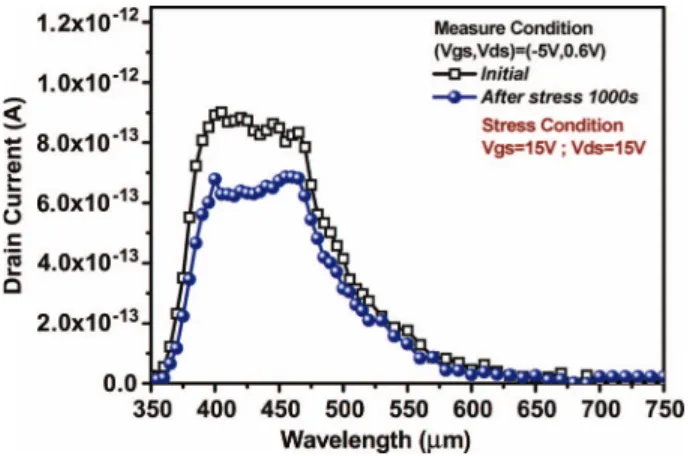
Considering that the poly-Si TFTs are derived after self-heating degradation, Fig. 14 shows the band diagrams under the condition of Vg < 0 along the channel direction near the drain region at high drain biases. The symbols at midgap energy level are additional nonuniform defects. When the devices are de-rived after self heating stress, the high temperature in the poly-Si film can release hydrogen and cause plenty of dangling bonds
Fig. 15. Photo leakage current spectrum of the light source in the range of 350–750 nm at lower bias after self-heating stress.
to become deep states. These deep states near the mid level, in the lateral depletion region, can recombine the electron–hole pairs generated by irradiation. Although the photo-induced carriers might also excite due to the extra defects, the total current is eventually reduced by much recombination deep states. Fig. 15 provides the photo leakage current spectrum of the light source in the range of 350–750 nm at lower bias after self heating stress. It is noticed that the photo leakage current certainly decreased. On the other hand, in the gate–drain overlap depletion region, the hole concentration of the chan-nel/LDD junction formed an abrupt p+n−junction accumulated
by the gate electrodes. The accumulated holes captured by the extra deep states in the gate–drain overlap region slightly allow hole concentration. It makes channel/LDD junction with an abrupt high–low junction (p+pn− junction in this case). In addition, the p+p junction forms a low-resistance ohmic contact for majority carriers (holes). The minority carriers (electrons) therefore considered relatively lower recombination velocity. This phenomenon causes ULC2 to not dramatically decrease
after self heating stress.
IV. CONCLUSION
In this paper, we have applied hot carrier and self-heating stress conditions to correlate the photosensitivity with different types of defects on LTPS TFTs. This analysis allows us to understand the role of the different types of defects that result in anomalous photo current. Furthermore, based on both trap-assisted and Poole–Frenkel effects, a modified defect-related ULC model for TFT has been proposed to explain the illumina-tion behaviors corresponding to the defects created by dc stress near the drain region. The empirical equation of ULC provides a potential modeling for simulation of LTPS TFT circuitry considering the photo effect after dc stress.
REFERENCES
[1] Y. H. Tai, C. C. Pai, B. T. Chen, and H. C. Cheng, “A source-follower type analog buffer using poly-Si TFTs with large design windows,” Electron.
Lett., vol. 26, no. 11, pp. 813–881, Nov. 2005.
[2] F. Matsuki, K. Hashimoto, K. Sano, D. Yeates, J. R. Ayres, M. Edwards, and A. Steer, “Integrated ambient light sensor in LTPS AMLCDs,” in
Proc. Soc. Inf. Display, 2007, pp. 290–293.
[3] H. S. Lim and O. K. Kwon, “Ambient light sensing circuit using LTPS TFTs for auto brightness control,” in Proc. Workshop Active-Matrix Flat
Panel Displays Devices, 2006, pp. 21–24.
[4] S. Koide, S. Fujita, T. Ito, S. Fujikawa, and T. Matsumoto, “LTPS am-bient light sensor with temperature compensation,” in Proc. Int. Display
Workshop, 2006, pp. 689–690.
[5] M. Inoue and H. Ohshima, “LTPS technologies for advanced mobile dis-play applications,” in Proc. Workshop Active-Matrix Flat Panel Disdis-plays, 2007, pp. 215–219.
[6] C. Brown, H. Kato, K. Maeda, and B. Hadwen, “A CG silicon system LCD with optical input function,” in Proc. Int. Display Workshop, 2000, pp. 99–103.
[7] T. Eguchi, Y. Hiyoshi, E. Kanda, H. Sera, T. Ozawa, T. Miyazawa, and T. Matsumoto, “A 1300-dpi optical image sensor using an a-Si:H photo diode array driven by LTPS TFTs,” in Proc. Soc. Inf. Display, 2007, pp. 1097–1100.
[8] T. T. Fuyuki, K. Kitajima, H. Yano, T. Hatayama, Y. Uraoka, S. Hashimoto, and Y. Morita, “Thermal degradation of low temperature poly-Si TFT,” Thin Solid Films, vol. 487, no. 1/2, pp. 216–220, Sep. 2005. [9] Y. H. Tai, S. C. Huang, C. W. Lin, and H. L. Chiu, “Degradation of the capacitance voltage behaviors of the low-temperature polysilicon TFTs under DC stress,” J. Electrochem. Soc., vol. 154, no. 7, pp. 611–618, May 2007.
[10] Y. H. Tai, Y. F. Kuo, and Y. H. Lee, “Photosensitivity analysis of low-temperature poly-Si thin-film transistor based on the unit-lux-current,”
IEEE Trans. Electron Devices, vol. 56, no. 1, pp. 50–56, Jan. 2009.
[11] W. J. Wu, R. H. Yao, S. H. Li, Y. F. Hu, W. L. Deng, and X. R. Zheng, “A compact model for polysilicon TFTs leakage current including the Poole Frenkel effect,” IEEE Trans. Electron Devices, vol. 54, no. 11, pp. 2975– 2983, Nov. 2007.
[12] Y. H. Tai, Y. F. Kuo, and Y. H. Lee, “Dependence of photosensitive effect on the defects created by DC stress for LTPS TFTs,” Electron. Lett., vol. 29, no. 12, pp. 1322–1324, Dec. 2008.
[13] J. H. Chen, S. C. Wong, and Y. H. Wang, “An analytic three-terminal band-to-band tunneling model on GIDL in MOSFET,” IEEE Trans. Electron
Devices, vol. 48, no. 7, pp. 1400–1405, Jul. 2001.
[14] C. S. Chuang, T. C. Fung, B. G. Mullins, J. Kanicki, K. Nomura, T. Kamiya, H. Hosono, and H. P. Shieh, “Photosensitivity of amorphous IGZO TFTs for active-matrix flat-panel displays,” in Proc. Soc. Inf.
Dis-play, 2008, pp. 1215–1218.
[15] J. R Ayres, S. D Brotherton, I. R Clarence, and P. J. Dobson, “Photocur-rents in poly-Si TFTs,” Proc. Inst. Elect. Eng.—Circuits, Devices Syst., vol. 141, no. 1, pp. 27–32, Feb. 1994.
[16] N. P. Papadopoulos, A. A. Hatzopoulos, D. K. Papakostas, C. A. Dimitri-adis, and S. Siskos, “Modeling the impact of light on the performance of polycrystalline thin-film transistors at the sub-threshold region,”
Micro-electron. J., vol. 37, no. 11, pp. 1313–1320, Nov. 2006.
[17] C. H. Kim, K.-S. Sohn, and J. Jang, “Temperature dependent leakage currents in polycrystalline silicon thin film transistors,” J. Appl. Phys., vol. 81, no. 12, pp. 8084–8090, Jun. 1997.
[18] G. Fortunato and P. Migliorato, “Determination of gap state density in polycrystalline silicon by field-effect conductance,” Appl. Phys. Lett., vol. 49, no. 16, pp. 1025–1027, Oct. 1986.
[19] O. K. B. Lui and P. Migliorato, “New generation-recombination model for device simulation including the Poole–Frenkel effect and phonon-assisted tunnelling,” Solid State Electron., vol. 41, no. 4, pp. 575–583, Apr. 1997.
Ya-Hsiang Tai (M’06) received the B.S. and Ph.D.
degrees in electronic engineering from the National Chiao Tung University, Hsinchu, Taiwan, in 1990 and 1996, respectively.
In 2000, he was with Prime View International, where he was involved in low-temperature poly-crystalline silicon (LTPS) thin-film transistor (TFT) development. In 2001, he was with Toppoly Opto-electronics Corporation, where he led the team of LTPS TFT LCD panel design. Since 2003, he has been a Faculty Member with the National Chiao Tung University, where he is currently an Associate Professor with the Depart-ment of Photonics and Display Institute. His current research emphases include TFT device physics, active matrix display panel design, and system on panel.
Dr. Tai is a member of Phi Tau Phi. He was a member of the Industrial Technology Research Institute/Electronics Research and Service Organization and became part of the TFT LCD development as a Panel Designer.
1022 IEEE TRANSACTIONS ON ELECTRON DEVICES, VOL. 57, NO. 5, MAY 2010
Yan-Fu Kuo received the B.S. degree in physics
in 2002 from the National Sun Yat-Sen University, Kaohsiung, Taiwan, and the M.S. degree in elec-trooptical engineering in 2004 from the National Chiao Tung University, Hsinchu, Taiwan, where he is currently working toward the Ph.D. degree.
He is currently with the Department of Photon-ics and the Institute of Electro-Optical Engineering, National Chiao Tung University. His current interests include sensors and applications of low-temperature poly-Si TFTs.
Guo-Pei Sun received the B.S. degree in
optoelec-tronics and communication engineering from the National Kaohsiung Normal University, Kaohsiung, Taiwan, in 2007 and the M.S. degree from the National Chiao Tung University, Hsinchu, Taiwan, in 2009.
She is currently with the Department of Photonics and Display Institute, National Chiao Tung Univer-sity. Her research interest is light sensing functions of low-temperature poly-Si TFTs.