Formation of stacked nickel-silicide nanocrystals by using a co-mixed target
for nonvolatile memory application
Wei-Ren Chen
a, Ting-Chang Chang
b,⁎
, Po-Tsun Liu
c, Chun-Hao Tu
a, Feng-Weng Chi
d,
Shu-Wei Tsao
d, Chun-Yen Chang
aaInstitute of Electronics, National Chiao Tung University, Hsin-Chu, Taiwan 300, Republic of China
bDepartment of Physics and Institute of Electro-Optical Engineering, Center for Nanoscience and Nanotechnology, National Sun Yat-set University,
70 Lien-hai Road, Kaohsiung 80424, Taiwan, Republic of China
cDepartment of Photonics & Display Institute, National Chiao Tung University, Hsin-Chu, Taiwan 300, Republic of China d
Department of Physics, National Sun Yat-Sen University, Taiwan, Republic of China Available online 17 August 2007
Abstract
The formation of stacked nickel-silicide nanocrystals by using a co-mixed target is proposed in this paper. High resolution transmission electron microscope analysis clearly shows the stacked nanocrystals embedded in the silicon oxide after rapid thermal oxidation. The obvious memory window can be used to define“1” and “0” states at low voltage operation. In addition, the program/erase characteristics have different charge/discharge efficiency due to the effect of stacked structure. Furthermore, good endurance and retention characteristics are exhibited for nonvolatile memory application. Besides, this technology is suitable for the fabrication of current nonvolatile memory and application of low power device.
© 2007 Elsevier B.V. All rights reserved.
Keywords: Metal nanocrystal; Nonvolatile memory; Nickel-silicide
1. Introduction
The conventional floating gate (FG) memories have been widely applied to portable electronic products, such as mobile phones, digital cameras, notebook computers, smart cards, personal digital assistant (PDA), and USB flash etc. [1]. The requirements of further scaling down nonvolatile memory (NVM) are the high density cells (memory capacity), low power consumption, high-speed operation and good reliability[2,3]. However, all of the charges stored in the FG will leak into the substrate if there is a leakage path generated in the tunnel oxide in the conventional FG memory, due to endurance test or hot carriers writing process. Thus, the thickness of tunnel oxide is difficult to scale down for the consideration of charge retention and endurance characteristics[3,4]. To overcome this problem, memory-cell structures employing discrete traps as the charge storage media have been attracted for the promising candidates
to replace conventional FG memory[2–5]. Recently, the metal nanocrystal NVM with separated charge trapping centers was extensively investigated, because of several advantages, such as stronger coupling with the conduction channel, higher density of state than semiconductor and a wide range of available work functions [6]. In the present research, the nickel-silicide nanocrystal (work function∼5.0–4.7 eV) was formed using a self-assembled method that oxidized thin nickel-silicide layer to segregate nanocrystal by different temperatures[7]. However, it is difficult to uniformly control the component of deposited nickel-silicide thin film using co-sputtering method (two targets used) and electron-beam evaporation. The size and uniformity of nickel-silicide nanocrystal therefore were critically affected by a ratio of silicon (Si) and nickel (Ni)[8]. This study proposes the formation of stacked nickel-silicide nanocrystal by using a co-mixed target (Ni0.3Si0.7) for nonvolatile memory application. The component of the nickel-silicide thin film can be well-controlled by a co-mixed target with a fixed component ratio. A suitable component ratio can be simple to form nickel-silicide nanocrystal after rapid thermal oxidation process.
Surface & Coatings Technology 202 (2007) 1292–1296
www.elsevier.com/locate/surfcoat
⁎ Corresponding author.
E-mail address:[email protected](T.-C. Chang). 0257-8972/$ - see front matter © 2007 Elsevier B.V. All rights reserved. doi:10.1016/j.surfcoat.2007.07.101
2. Experimental procedure
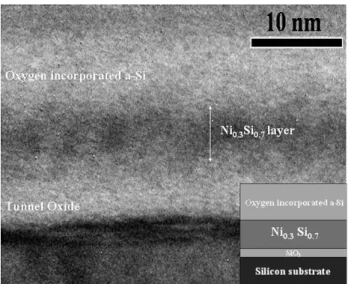
A metal-insulator-semiconductor-device used in this work includes a tri-layer insulator structure on a Si substrate. First, the 4 in p-type Si wafers with (100) orientation were cleaned with a standard RCA process, followed by a dry oxidation process in an atmospheric pressure chemical vapor deposition (APCVD) furnace to form a 3-nm-thick tunnel oxide. Afterwards an 8-nm-thick Ni0.3Si0.7 layer was deposited onto the tunnel oxide by sputtering a Ni0.3Si0.7target at the 80 W DC power. Then this Ni0.3Si0.7layer was capped by a 20-nm-thick amorphous Si (a-Si) layer by sputtering a Si target in the oxygen environment. This step can obtain an oxygen-incorporated a-Si layer as shown inFig. 1. A rapid thermal oxidation (RTO) at 500 °C for 30 s was executed to oxidize the oxygen-incorporated a-Si layer and leading to improved quality of blocking oxide. In addition, the deposited Ni0.3Si0.7layer was precipitated to nickel-silicide nanocrystals and the remaining Si were oxidized to isolate the nickel-silicide na-nocrystals during a foregoing RTO process[9]. Al gate electrode was finally patterned to form metal/oxide/insulator/oxide/Si (MOIOS) structure. High resolution transmission electron micro-scope (HRTEM) and Auger electron spectroscopy (AES) were adopted for the micro-structure analysis and Ni-atom depth distri-bution analysis. The electrical characteristics, including the current density–voltage (J–V), capacitance–voltage (C–V) hysteresis, program/erase efficiency, retention and endurance characteristics were also performed. The J–V and C–V characteristics were measured by Keithley 4200 and HP4284 Precision LCR Meter with high frequency 100 kHz.
3. Results and discussions
Fig. 1 shows a cross-sectional HRTEM of the Si substrate/
tunnel oxide/Ni0.3Si0.7 layer/oxygen-incorporated a-Si stacked structure. It is simply observed that the Ni0.3Si0.7layer (charge trapping layer) is uniform and its thickness is about 7–8 nm. After the RTO process, the spherical and separated nickel-silicide
nanocrystals with a size of 4–6 nm are clearly observed embedded in the SiO2layer, as shown inFig. 2(a). The distributed density of the nanocrystals can use HRTEM analysis to roughly estimate about 2.67 × 1012 cm− 2, due to stacked nanocrystals. The large charge storage ability at scale-down devices can be maintained for the stacked structure with nanocrystals embedded in dielectric
[10]. In addition, the size of nickel-silicide nanocrystals near the blocking oxide is obviously larger than that at the surface of tunnel oxide, due to the thermal driving of Ni-atom during the blocking oxide formation[11]. The schematic chart of a formation flow of the nickel-silicide nanocrystals after RTO operated at low temperature was shown inFig. 2(b). Furthermore, the retention characteristics can be also improved as electrons stored in the nanocrystals near the blocking oxide[12].
Fig. 3 exhibits the Auger electron spectroscopy (AES)
analysis of a tri-layer structure during RTO process. It is found that partial Ni-atom of Ni0.3Si0.7layer diffuses to blocking oxide
Fig. 1. Cross-sectional HRTEM analysis of a deposition for a Si substrate/tunnel oxide/Ni0.3Si0.7layer/oxygen-incorporated a-Si structure.
Fig. 2. (a) Cross-sectional HRTEM analysis of stacked nickel-silicide nanocrystals. The sizes of nanocrystals (from substrate to blocking oxide) and density are 4–6 nm and 2.67×1012cm− 2, respectively. (b) Schematic of the
deposited Ni0.3Si0.7layer precipitated to nanocrystals and oxygen-incorporated
a-Si layer oxidized to form blocking oxide during the RTO process. The arrow is to indicate thermal driving effect of Ni-atom during RTO process.
Fig. 3. Auger electron spectroscopy (AES) analysis of MOIOS structure with a deposition and after RTO treatment for Ni-atom depth distribution analysis.
after the RTO process due to the thermal driving effect of Ni-atom (as shown in region A ofFig. 3). This result is in agree-ment with the above-agree-mentioned discussion. Moreover, the low temperature RTO process is believed to effectively avoid Ni-atom to excessively out diffuse to blocking oxide for high diffusivity of Ni-atom[11]. Hence, the RTO process adopted on the proposed structure in this study can avoid the leakage paths that are produced by Ni dopant generated in the blocking oxide.
Fig. 4exhibits the capacitance–voltage (C–V) hysteresis after
the bidirectional voltage sweeping from 5 V to (−5) Vand (−5) V to 5 V. It is clearly indicated that a 1.77 V memory window can be obtained under a ±5 V operation, which is suitable for the appli-cation of low power device. It is perceived that the hysteresis is counterclockwise for p-type Si substrate, due to an injection of electrons from the deep inversion layer and discharge of electrons
from the deep accumulation layer[13]. In addition, the inset of
Fig. 4 exhibits that the current density–voltage (J–V) of the
MOIOS structure, and the current density is small enough to prevent storage charge loss.
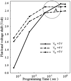
The program characteristics of MOIOS structure are shown inFig. 5. The flat-band voltage shift (ΔVFB) is increased with an increased program voltage/increased program duration. However, it is found that theΔVFBare saturated as the program duration is longer than 50 ms at the voltages of 4 V and 5 V. As compared to the 4 V and 5 V program operations, the larger memory window was found at a program voltage of 3 V for long program duration (as shown in region A ofFig. 5). As analyzed theoretically in previous research [14], there are two compo-nents of the electron current flow in the nanocrystals memory structure. One is the current between the substrate and the nanocrystals (Itun) and the other is between the nanocrystals and the control gate (Icon, as shown in the inset (J–VG) ofFig. 4).
Fig. 5. Program characteristics of nanocrystals memory at different gate program voltages with different program duration. Program gate voltage = (1) 5 V, (2) 4 V, and (3) 3 V.
Fig. 6. Erase characteristics of nanocrystals memory at different gate erase voltages with different erase duration. Erase gate voltage = (1)−5 V, (2) −4 V, and (3)−3 V.
Fig. 4. Capacitance–voltage (C–V) hysteresis of the MOIOS structure after the bidirectional voltage sweeps from 5 V to (−5) V and (−5) V to 5 V. The inset is current density characteristics (J–VG) of the MOIOS structure by voltage
sweeping from 0–N5 V and 0–N(−5) V.
Fig. 7. Endurance characteristics of stacked nanocrystals with 5 V for 500μs (program state) and−5 V for 900 ms (erase state).
TheΔVFBshould be saturated as Itunand Iconare at steady state. As the program voltage is increased, partial electrons are lost to gate electrode via Fowler–Nordheim tunneling and the trap assisted tunneling mechanism. The trap assisted tunneling process is dominated at high voltage operation for the oxidized a-Si serving as blocking oxide, due to obtaining a linear relation between ln(Icon) and gate voltage (3–5 V) by the trap assisted tunneling model[15]. The trap state generation is resulted from the low temperature formation of blocking oxide (oxidized oxygen-incorporated a-Si layer). A lot of charge storage centers are thereby formed in the stacked nanocrystals-embedded device structure. However, the exceed program voltage cause the saturated memory effect for long program duration due to the easier leakage path at high operation voltage.
The erase characteristics are shown inFig. 6. The flat-band voltage shift (ΔVFB) is decreased as the erase voltage increased at the same erase duration, and also decreased with the increasing erase duration at the same erase voltage. However, it is found that theΔVFBshift of 0.5 V can be achieved as the erase voltage is−5 V and erase time is 10 ms. It is considered that partial carriers stored in the nanocrystal near the blocking oxide are difficult to erase. Hence, larger erase voltage (N−5 V) for the stacked nanocrystals structure is needed to perform shorter erase time for further nonvolatile memory application.
Fig. 7 shows the endurance characteristics of the stacked
structure obtained after cycling the structure between 5 V for 500μs (program state) and −5 V for 900 ms (erase state). The cycling was interrupted at 105 cycles and C–V measurements were recorded. Furthermore, the MOIOS structure with stacked nanocrystals tolerates approximately 106 cycles and memory window remains about 0.8 V (degradation 11% after 106cycles), which is considered satisfactory for the used duty cycle.
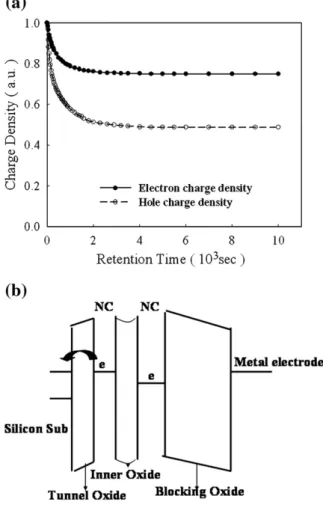
The charge retention characteristics for the proposed nickel-silicide nanocrystal NVM are shown inFig. 8(a). The retention characteristics were investigated at room temperature using ±5 V gate voltage stress for 10 s and the charge density was estimated by C-t (capacitance to time) measurements[16]. When carriers are stored in the nanocrystals, the stored charges will raise the nano-crystal potential energy and increase the probability of escaping from the nanocrystal to Si substrate [17]. Moreover, a sample schematic band diagram for charge stored in stacked structure with nickel-silicide nanocrystals embedded in dielectric layer explained the phenomenon of charge loss, as shown inFig. 8(b). The nanocrystals located near the tunnel oxide have higher quantized energy states, due to smaller size of nanocrystal, which causes the easy escaping path[12,18]. Therefore, the electron and hole density are observed to decay exponentially with time before 1000 s, resulting in charge loss of 20% for electrons and 50% for holes. It can also be observed that the hole has lower charge density than electron. Because some holes are stored in shallow trap states of SiOxaround the nanocrystals, they are unstable and easy to escape from shallow trap states of SiOxto Si substrate[19]. However, partial carriers can be conserved and the memory window also can be retained at 1.9 V for electrons density and 1.2 V for holes density, respectively. It is considered that the metal nanocrystals have larger work function than Si substrate. In addition, the carriers that are stored in the nanocrystals can be
extrapolated to keep up to 10 years by using extrapolation method to fit stable state of retention.
4. Conclusion
In conclusion, the stacked nickel-silicide nanocrystals memory was fabricated by sputtering a co-mix target followed by a low temperature (at 500 °C for 30 s) RTO process. A larger memory window of 1.77 V was observed after ± 5 V voltage sweep. The trap states in blocking oxide cause the larger memory effect at low voltage as the memory window is saturated at high program voltage. The endurance and date retention of the nanocrystal memory device are also good enough to maintain unto 106cycles and 10 years. In addition, the rapid thermal oxidation at low temperature can greatly reduce the thermal budget for the fabri-cation of the current nonvolatile memory.
Acknowledgements
This work was performed at National Nano Device Laboratory and was supported by the National Science Council of the Republic of China under Contract nos. NSC 96 2221 E 009 -202 - MY3, and NSC 96 - 2120 - M - 110 - 001. Furthermore, this work was partially supported by MOEA Technology
Fig. 8. (a) Charge retention characteristics of stacked structure with nickel-silicide nanocrystals. (b) A sample schematic band diagram of stacked nanocrystals structure under retention state. The electrons stored in the nanocrystal near the tunnel oxide are easily escaped from nanocrystals to Si substrate.
Development for Academia Project# 94-EC-17-A-07-S1-046 and MOE ATU Program“Aim for the Top University” #95 W803. References
[1] S. Tiwari, F. Rana, K. Chan, H. Hanafi, W. Chan, Doug Buchanan, IEDM Tech. Dig. (1995) 521.
[2] P. Pavan, R. Bez, P. Olivo, E. Zanoni, Proc. IEEE. 85 (1997) 1248. [3] D. Kahng, S.M. Sze, Bell Syst. Tech. J. 46 (1967) 1288.
[4] T.Y. Chan, K.K. Young, C. Hu, IEEE Electron Device Lett. 8 (1987) 93. [5] N.M. Park, S.H. Choi, S.J. Parka, Appl. Phys. Lett. 81 (2002) 6. [6] Z. Liu, C. Lee, V. Narayanan, G. Pei, E.C. Kan, IEEE Trans. Electron
Devices. 49 (2002) 1606.
[7] P.H. Yeh, H.H. Wu, C.H. Yu, L.J. Chen, P.T. Liu, C.H. Hsu, T.C. Chang, J. Vac. Sci. Technol. 23 (2005) 4.
[8] J.H. Yoona, G.H. Lee, R.G. Elliman, J. Appl. Phys. 99 (2006) 116106. [9] C.J. Tsai, K.H. Yu, Thin Solid Films 350 (1999) 91.
[10] C.Y. Ng, T.P. Chen, L. Ding, S. Fung, IEEE Electron Device Lett. 27 (2006) 4. [11] F. d'Heurle, C.S. Petersson, J.E.E. Baglin, S.J. La Placa, C.Y. Wong,
J. Appl. Phys. 55 (1984) 12.
[12] L.C. Wua, K.J. Chen, J.M. Wang, X.F. Huang, Z.T. Song, W.L. Liu, Appl. Phys. Lett. 89 (2006) 112118.
[13] D.N. Kouvatsos, V.L. Sougleridis, A.G. Nassiopoulou, Appl. Phys. Lett. 82 (2003) 397.
[14] C.M. Compagnoni, D. Ielmin, A.S. Spinelli, A.L. Lacaita, IEEE Trans. Electron Devices 52 (2005) 4.
[15] M. Houssa, M. Tuominen, M. Naili, V. Afanas'ev, A. Stesmans, S. Haukka, M.M. Heyns, Appl. Phys. Lett. 87 (2000) 12.
[16] C.H. Cho, B.H. Kim, T.W. Kim, S.J. Park, N.M. Park, G.Y. Sung, Appl. Phys. Lett. 86 (2005) 143107.
[17] C.W.J. Beenakker, Phys. Rev. B. 44 (1991) 1646. [18] T. Takagahara, K. Takeda, Phys. Rev. B. 46 (1992) 15578.
[19] C.Y. Ng, T.P. Chen, M. Yang, J.B. Yang, L. Ding, C.M. Li, A. Du, A. Trigg, IEEE Electron Device Lett. 53 (2006) 4.