positive shifts. By employing simulation, it was proved that the self-heating effect creates interface states near the source region and increases the deep states in the poly-Si film near drain. The proposed circuit model further explains the behavior of the CGS and CGDcurves for the stressed device at different measuring frequencies.
© 2007 The Electrochemical Society. 关DOI: 10.1149/1.2735921兴 All rights reserved.
Manuscript submitted October 13, 2006; revised manuscript received February 6, 2007. Available electronically May 15, 2007.
Low-temperature poly-Si 共LTPS兲 thin-film transistors 共TFTs兲 have attracted much attention for active matrix liquid crystal display 共AMLCD兲 and active matrix organic light emitting diode 共AMOLED兲 applications due to the high mobility and capability of realizing integrated circuits on the same glass. The degradation be-havior of the device is an important issue in the application. It was reported that poly-Si TFTs suffer from several degradation mecha-nisms, such as hot carrier effect,1-4 self-heating effects,5,6 water,7 and photon-induced leakage current.8,9 The two main degradation mechanisms of n-type TFTs are the hot carrier effect and the self-heating effect.10 Hot carrier effect, arising from the carriers under the high electric field around the drain, is reported to cause the degradation of drain current and channel mobility.11 In poly-Si TFTs, because there are many traps in the poly-Si film, the hot carrier effect is closely related to the crystallization condition and grain boundary locations of the poly-Si film.12The degradation of threshold voltage and mobility of devices after self-heating stress is especially a serious problem, because TFTs are fabricated on glass substrates which have the poor thermal conductivity. Most of the previous works focused on the current transfer characteristics to investigate the mechanism of degradation after stress. However, be-cause the current transfer behaviors are affected by the entire deg-radation regions in the channel, it would be difficult to examine the damaged region of the device after stress in detail. In this work, the effects of these two stress conditions are examined with capacitance-voltage共C-V兲 measurement, which can further reveal the damaged location and mechanism of these two stress conditions. The fre-quency response of the capacitance curves would also be helpful in identifying the degradation mechanisms to be the trapped charges or the increased states.
Experimental
The process flow of TFTs is described below. First, the buffer oxide and 50 nm thick a-Si:H films were deposited on glass sub-strates with plasma-enhanced chemical vapor deposition共PECVD兲. The samples were then put into the oven for dehydrogenation. The XeCl excimer laser of wavelength 308 nm and energy density of 400 mJ/cm2was applied. The laser scanned the a-Si:H film with the beam width of 4 mm and 98% overlap to recrystallize the a-Si:H film to poly-Si. After poly-Si active area definition, 80 nm SiO2and 40 SiNx films were deposited with PECVD as the gate insulator.
Next, the metal gate was formed by sputter and then defined. The lightly doped drain 共LDD兲 and the n+ source/drain doping were formed by PH3 implantation with dosage 2⫻ 1013 and 2 ⫻ 1015cm2of PH
3, respectively. The LDD implantation was self-aligned and the n+regions were defined with a separate mask. Then the interlayer of SiNx was deposited. Subsequently, the rapid ther-mal annealing was conducted to activate the dopants. Meanwhile, the poly-Si film was hydrogenated. Finally, the contact hole forma-tion and metallizaforma-tion were performed to complete the fabricaforma-tion work.
In this study, n-type TFTs with a channel width of 20m and a channel length of 5m with an LDD structure of length 1.2 m are fabricated. The C-V curves of the gate-to-source capacitance CGS and gate-to-drain capacitance CGDbefore and after stress with dif-ferent frequencies are measured with an HP 4284A precision LCR meter. The concept of operation of the apparatus is to find the effec-tive impedance of the equivalent circuit of the device under test between the probing nodes, and via the circuit theory, the capaci-tance of the device can then be obtained. Before measuring the capacitance behavior, for every frequency the measure correction is performed with the open-circuit and short-circuit mode, respectively, for the needles before and after probing the electrode to eliminate the effect of the parasitic components in the surrounding and during probing.
Results and Discussion
Hot carrier effect.— Hot carrier effect, as many works have re-ported, is closely related to the distribution of the lateral electric field in the channel and therefore is in relation with the applied drain voltage VDS and gate voltage VGS. The high electric field near the drain region would accelerate the carriers and these carriers may break the Si bonds, resulting in the increase of tail states. These increased states affect the conduction for the gate voltage larger than the threshold voltage VTHand then degrade the device mobility.13 Unlike in metal oxide semiconductor field effect transistors 共MOS-FETs兲, the hot carrier effect in TFTs becomes most severe as VGSis just above VTHand VDSis large.14Because the active region in the poly-Si TFTs contains many grain boundaries, the effect of hot car-rier stress may be more complicated than that in MOSFETs. Figure 1 shows the ID-VGtransfer characteristics before and after 500 s of hot carrier stress with the conventional forward and reverse connec-tion. Here the stress condition is that the drain voltage is equal to 20 V and the gate voltage is 1 V larger than VTH, namely, 2.8 V. It can be seen that as compared with the unstressed device, the stressed
z
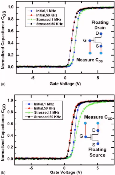
device shows lower ON current and almost unchanged subthreshold region. However, the difference in the ON current of the stressed device between the forward and reverse connection indicates that the states distribute closer to the drain. In order to understand the detailed degradation mechanism, C-V measurement is employed. Figure 2a shows the normalized gate-to-source capacitance CGS curves before and after stress with different measuring frequencies, and Fig. 2b shows those of the CGD curves. The CGS is measured with the floating drain and CGDis measured with the floating source. The normalized capacitance is the ratio of the measured capacitance to a constant of 40 fF, which is the gate insulator capacitance of the TFT. The CGScurves of the stressed device show almost no differ-ence as compared with the unstressed device. Nevertheless, the CGD curves of the stressed device show peculiar behaviors. The CGD curve of the stressed device measured at 50 kHz is almost the same as that before stress, but the curve at 1 MHz shows that the apparent stretch for the gate voltage is just above the flatband voltage VFB. In other words, the degradation behavior of the CGD curves of the device after hot carrier stress is frequency dependent.
In order to examine the frequency dependence of the C-V behav-ior of the devices after hot carrier stress, the CGSand CGDcurves of the stressed devices at different applied frequencies are measured. Figures 3a and b show the CGS and CGD curves of the stressed device at measuring frequencies of 50 kHz, 100 kHz, 500 kHz, and 1 MHz. The CGS curves of the stressed device show only a slight shift for different applied frequencies. However, in addition to the shift, the CGD curves show an apparent stretch between different measuring frequencies for the gate voltage higher than VFB. The higher the measuring frequency applied, the more the CGD curve stretches.
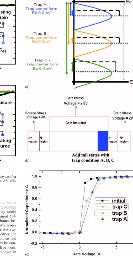
To find the mechanism of this behavior, the 2D simulation pro-gram DESSIS is employed. The grain boundaries inside the poly-Si film are accounted for by using the “effective medium approach,” which treats the poly-Si film as a uniform material with the density of localized states in the bandgap.15Referring to previous reports, the hot carrier effect causes the increase of the tail states in the bandgap of the poly-Si film.16Therefore, in simulation the tail states are purposely simulated with the Gaussian distribution in the band-gap of the poly-Si film near the drain. Figures 4a and b, respectively, show the state condition in the bandgap and physical location in the simulation. The tail states are modeled by the Gaussian distribution with standard deviation 0.2 eV and the peak value of the distribution is 1020cm−3. Three kinds of state positions in the bandgap of 0.6 eV are arranged in simulation. The three state conditions are arranged such that the distance between the bottom of the conduction band EC and the center of the state distributions are 0.2, 0.3, and 0.4 eV.
Figure 4c is the simulated C-V curves of the proposed device model with the three state conditions. It can be seen that the capacitance curve would apparently stretch for the gate voltage just above VFB for the trap condition C, which is the state distribution located just above the Fermi level EF. When the state locations are drawn near to EC, as in the case of state conditions A and B, the capacitance curves would stretch more for the gate voltage larger thanVFB.
The simulated curves may fairly explain the capacitance curves for the high measuring frequency, but it may not explain the capaci-tance curves for different applied frequencies. With the viewpoint of trap and emission, the states in the channel would have enough time to respond to the applied signal at lower measuring frequency and thus the effect of the states can be measured. However, the measured results show the opposite behavior. In order to explain the frequency dependence of the capacitance behavior after stress, a circuit model considering channel resistances and gate insulator capacitances is proposed, as shown in Fig. 5a. For the unstressed device, the model is composed of the distributed insulator capacitance共Cin兲, channel resistance 共Rch兲, junction capacitance 共Cj兲, and contact resistance 共RC兲. The C-V behavior and the I-V behavior can be correlated by considering the impedance of the device in this model. As the gate voltage is much higher than VTH, the channel resistance will become very small and the nodes in the channel can be viewed as short-circuited. At this time, the total impedance would be dominated by the gate insulator capacitance and all the distributed capacitance can Figure 1.共Color online兲 Current-transfer characteristics before and after hot
carrier stress condition共VGS= Vth+ 1 V = 2.8 V, VDS= 20 V, and time du-ration of 500 s兲 with the forward and reverse connections.
Figure 2.共Color online兲 共a兲 and 共b兲 Normalized CGSand CGDcurves共before and after hot carrier stress兲 vs gate voltage at frequencies of 50 kHz and 1 MHz.
H612 Journal of The Electrochemical Society, 154共7兲 H611-H618 共2007兲
be measured. In other words, the measured capacitance would be the summation of all the gate insulator capacitances. As the gate voltage is far below VTH, the channel resistances are so high that they would block the signal deep in the channel. Therefore, the measured C-V behavior in this region may actually represent the capacitance be-haviors only near the edges of the channel, which may only repre-sent the capacitance of the overlapped region between the two probed electrodes. However, for the transient region, neither the resistance nor the capacitance would dominate the impedance and hence both the effects of capacitance and resistance should be con-sidered. Because the capacitive impedance is frequency dependent, the frequency dependence of the measured C-V curves shown in Fig. 3 can thus be inferred.
Figures 5b show the simulated and measured curves of the nor-malized capacitance CGS for frequency 50 kHz and 1 MHz, while Fig. 5c shows those of the CGD curves for the fresh device. The simulation of the curves is calculated from the effective impedance of the proposed model between the probed nodes with the simple math tool. To start with, first the RDScurves are extracted from the ID-VGcurves with the drain voltage at 0.1 V to find the uniform-distributed channel resistance for every gate voltage. The effective impedance between the two nodes can then be calculated with the proposed model. Via circuit theory, the capacitance between the nodes can be calculated from the real and imaginary parts of the
effective impedance. For example, the simulation curves of CGSare calculated from the effective impedance between the gate and source electrode. For the simulated curves, it can be seen that the curves for different frequencies can well depict the capacitance behavior for the positive gate voltage with the use of the simple math calculation Figure 3.共Color online兲 Normalized CGSand CGDcurves for the device after
hot carrier stress with different frequencies of 50 kHz, 100 kHz, 500 kHz, and 1 MHz.
Figure 4. 共Color online兲 The model describing the device after hot carrier stress with the state condition in共a兲 the bandgap and 共b兲 the physical loca-tion, and共c兲 the simulated C-V curves for different state conditions.
tool, especially for 1 MHz frequency. This reveals that the capaci-tance behavior for different frequencies may just be the effect of the capacitances measured with the varying channel resistance at differ-ent gate voltages, which justifies the proposed model.
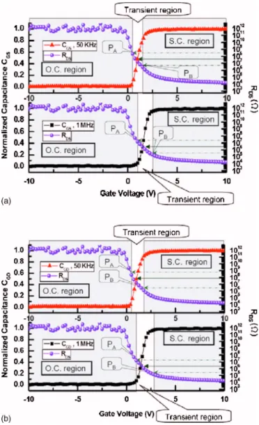
Figures 6a and b show the normalized CGSand CGDcurves and the total resistance RDS at different C-V measuring frequencies, where RDSis extracted from the ID-VGcurves at VD= 0.1 V. For the gate voltage around VTH, the channel resistance would go through a transient region and the magnitude of the channel resistance would rapidly decrease from around 109to 104⍀. A critical point of the
impedance behavior Pccan be selected as the channel resistance Rch equals the capacitance term 1/2fCin, which falls in the transient region of the CGS and CGD curves for the measuring frequency 50 kHz and 1 MHz. The term f represents the measuring frequency. The solid arrow in Fig. 6 represents the point that the total channel resistance RDSequals the capacitance term 1/2f CTFTfor different C-V measuring frequencies, where CTFTis about 40 fF, representing the gate insulator capacitance of the TFT. The upper dashed arrow represents the point PAwhere the channel resistance RDSis 10 times Figure 5.共Color online兲 共a兲 The proposed circuit model of the fresh poly-Si TFTs. 共b兲 Simulated curves for the CGScurves for the fresh device with frequency of 1 MHz and 50 kHz.共c兲 Simulated curves for the CGDcurves for the device with frequency of 1 MHz and 50 kHz.
H614 Journal of The Electrochemical Society, 154共7兲 H611-H618 共2007兲
larger than the capacitance term, and the lower dashed arrow repre-sents the point PB when the channel resistance Rch is 10 times smaller. In Fig. 6, the dashed arrows respectively point out the 80 and 4 M⍀ of the RDScurve, which correspond to the impedance of CTFTat the applied frequencies of 50 kHz and 1 MHz. For the gate voltage lower than PA, the conductivity of the device is considered to be low enough that the channel resistance can be taken as open circuit and is labeled as the “O.C. 共open-circuit兲 region.” For the gate voltage larger than PB, the channel becomes highly conductive to be considered as short circuit and is labeled as the “S.C. 共short-circuit兲 region.” Meanwhile, for the gate voltage between PAand PB, because the capacitive term and the resistive term of the imped-ance are comparable, neither of them can be ignored.
Figures 7a show the circuit model for the device after hot carrier stress. The terms Cdegand Rch,degrepresent the increase of the ca-pacitance and resistance due to the generated tail states during stress. Figure 7b shows the corresponding location in the bandgap of the capacitance Cdeg. Because the tail states are mainly related to the operation of the gate voltage above VTH, the state capacitance Cdeg would respond at the gate voltage larger than VFB. Under this gate voltage, the Fermi level is drawn near to the bottom of the conduc-tion band EC and then fills the capacitance Cdeg. Figures 8a and b show the normalized capacitance characteristics of CGS and CGD
with the total resistance RDSextracted from the ID-VGcurves for the device after hot carrier stress. For the low measuring frequency of 50 kHz, the capacitive term 1/2fCTFTis relatively larger than the channel resistance at the gate voltage slightly larger than VTH. Therefore the measured CGSand CGDcharacteristics would quickly contain the gate capacitance in the channel and saturate at CTFT. Hence, the effect of the degradation component Cdeg may not be obvious. However, for the high measuring frequency of 1 MHz, the channel resistance can be ignored until the gate voltage is much larger than VTHand thus the effect of the Cdegcomponents can be apparent. In other words, the degradation in the C-V behaviors for the device may only be observed at higher measuring frequencies, where the effect of the degraded capacitances can be obvious.
Self-heating effect.— Polysilicon TFTs, in most applications, are fabricated on glass substrates which have poor thermal conductivity. Therefore, as the applied VGSand VDS are high, the heat resulting from the high current flow and voltage difference in the channel may be difficult to dissipate. The accumulated heat causes the Si–H bonds to break, which in turn increases the deep states in the chan-nel. These states apparently affect the conduction of the device near the subthreshold and the ON region.5Most of the previous works focus on the current-transfer characteristics of the device after self-heating stress, while very few works mention the C-V behaviors of this mechanism.17In order to find the dominant mechanism and the corresponding circuit model, the C-V behavior of device after self-heating stress is examined and discussed in the following section.
Figure 9 shows the I-V transfer characteristics for the TFT before and after the 500 s of self-heating stress. The stress condition is that both VGSand VDSequal 18 V. For the stressed device, it can be seen that the threshold voltage VTHand the subthreshold swing increase, and the ON current decreases. Figure 10a shows the CGS curves before and after stress with different frequencies, while Fig. 10b shows the corresponding curves of CGD. Compared with the curves before stress, the stressed CGS and CGD curves exhibit two main changes, namely, the positive shift for the gate voltage near the flatband voltage VFBand the increase for the gate voltage just below VFB. The stretch and shift in the positive direction for the gate volt-Figure 6. 共Color online兲 共a兲 Normalized CGScurves and RDScurves at VD
= 0.1 V, and共b兲 the corresponding CGDand RDScurves for the fresh device.
Figure 7. 共Color online兲 共a兲 Proposed circuit structure for the device after hot carrier stress.共b兲 The corresponding location of Cdegin the bandgap.
age near VFB can be attributed to the increase of the deep states during stress. The increases of the C-V curves for the lower gate voltage possibly come from the interface states.
Figure 8. 共Color online兲 共a兲 Normalized CGScurves and RDScurves at VD = 0.1 V, and共b兲 the corresponding CGDand RDScurves for the device after hot carrier stress.
Figure 9. 共Color online兲 Current-transfer characteristics before and after self-heating stress condition 共VGS= VDS= 18 V, 500 s兲 with the forward and reverse connection.
Figure 10.共Color online兲 共a兲 and 共b兲 Normalized CGSand CGDcurves 共be-fore and after self-heating stress兲 vs gate voltage at frequencies 50 kHz and 1 MHz.
Figure 11.共Color online兲 The proposed degradation model in TFT structure with interface states and deep states.
H616 Journal of The Electrochemical Society, 154共7兲 H611-H618 共2007兲
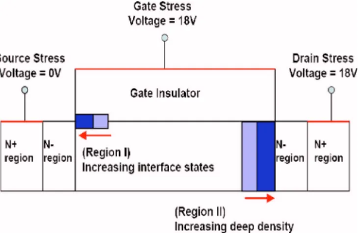
To verify this inference, a 2D numerical simulation program DESSIS is applied again to simulate the device characteristics. The model of the cross section of the device after self-heating stress is shown in Fig. 11. The deep states in the poly-Si film are modeled by a Gaussian distribution near the midgap. The peak value of the deep state density changes from 5⫻ 1018to 3⫻ 1017cm−3in the range of 0.3 um from the drain edge, corresponding to the temperature distribution during self-heating stress.18 The interface states of 1 ⫻ 1015cm−2 decreasing to 1⫻ 1014cm−2 are spatially arranged from the source edge, reflecting the electric field between the gate and source during stress. Figure 12 shows the simulation results with different degraded regions in the device. Curve A is the C-V curve with no degraded region, while curve B is the one with inter-face states near the source region. Comparing to curve A, curve B increases drastically for the gate voltage below VFB. This reveals that the interface states between the source and gate influence the induced carriers in the channel depletion and weak inversion re-gions. Curve C further includes the increase of deep states in the poly-Si film near the drain. The difference from curve B is that the curve stretches and shifts in the positive direction near VFB. The similarity between the simulated curves and the measured CGSand CGD curves reveals that the proposed model for the device after self-heating stress should be correct and applicable. However, the different degree of the increase of the CGSand CGDcurves at lower gate voltage still may not be explained by the simulation results.
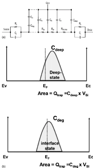
Figure 13a shows the proposed circuit model of the device after self-heating stress. The capacitance Cdeep is added to the device, representing the increase of the deep states during stress. In addition, Cdegis also introduced to represent the capacitance corresponding to the interface states induced by the high voltage difference VGS dur-ing stress. Figure 13b shows the corresponddur-ing location in the band-gap of the capacitance Cdeepand Cdeg. Because the deep states in the channel would affect the operation for the gate voltage near VFB, the position of Cdeepis located near the Fermi level EFin the bandgap. Because Cdegis found to influence the conduction for the gate volt-age below VFB, the corresponding position of Cdegis set to locate partly below EF. Figure 14a and b shows the normalized capacitance CGSand CGDand the total resistance RDSextracted from the ID-VG curves. In the O.C. region, because all the channel resistances are taken as opened, the model is reduced to only the capacitances in the device. Thus, the Cdeg resulting from the interface states and the Cdeepfrom the self-heating effect would lead to the increase of the CGSand CGDcurves for the lower gate voltage, respectively. In this region, the different frequency dependences for CGSand CGDcurves reflect the different responses of the states near the source and the drain, respectively. As the gate voltage increases, two effects make the CGSand CGDcurves change with gate voltage. First, the Fermi
level is drawn near to EC and the interface states are thus getting filled. Second, the channel resistance would also be gate voltage dependent. Hence, the stretch and shift of the C-V curves in the transient region may include the effect of the increase of the Cdeep and the decrease of Rch. For the higher gate voltages, all the states are filled and the channel resistances are very low, making the mea-sured capacitance CGS and CGD saturate at CTFT. The proposed model may fairly explain the frequency-dependent degradation of the capacitance curves after both the hot carrier and self-heating stress conditions. It would be of practical importance in further un-derstanding the reliability issues of LTPS TFTs.
Conclusion
In this work, the degradation of LTPS TFTs under hot carrier and self-heating stress was investigated using the C-V method. For the hot carrier stress, it is found that the degradation of the CGDcurves Figure 12.共Color online兲 Simulation results of the normalized C-V curves
with different state conditions共region I and region I and II兲.
Figure 13. 共a兲 The proposed circuit model of the poly-Si TFTs after self-heating stress.共b兲 The corresponding location of Cdegand Cdeepin the band-gap.
would exhibit apparent frequency dependence for different measur-ing frequencies. A circuit model connectmeasur-ing the I-V and C-V behav-iors is proposed to explain the anomalous C-V behavior. With this model, the C-V behaviors can be divided into three regions by com-paring the resistive term and the capacitive term of the total imped-ance. It is proposed that the frequency dependence of the CGD curves after hot carrier stress reflects the transient behaviors of the channel resistances and capacitances. In addition, it is discovered that the self-heating stress would cause the increase of deep states in
the poly-Si film near the drain and the interface states at the inter-face in the source region. The proposed model may further reveal that the measured capacitance exhibits the real capacitive behaviors of the states only in the O.C. regions, while the transient region reflects both the effects of resistances and capacitances. This finding would provide important information for further studies of the C-V behaviors and its relation to the I-V behaviors of LTPS TFTs.
Acknowledgments
This work was sponsored by the National Science Council, Re-public of China共NSC95-2221-E-009-229兲. This work was partially supported by the Ministry of Education Aim for the Top University 共MOE ATU兲 program and the Ministry of Economic Affairs 共MOEA兲 Technology Development Academia Project, no. 94-EC-17-A-07-S1-046.
National Chiao Tung University assisted in meeting the publication costs of this article.
References
1. I.-W. Wu, in Proceedings of AM-LCD 95, pp. 7–10共1995兲.
2. N. A. Hastas, C. A. Dimitriadis, J. Brini, and G. Kamarinos, IEEE Trans. Electron
Devices, 49, 1552共2002兲.
3. Y. Uraoka, T. Hatayama, T. Fuyuki, T. Kawamura, and Y. Tsuchihashi, Jpn. J. Appl.
Phys., Part 1, 40, 2833共2001兲.
4. T. Yoshida, Y. Ebiko, M. Takei, N. Sasaki, and T. Tsuchiya, Jpn. J. Appl. Phys.,
Part 1, 42, 1999共2003兲.
5. S. Inoue, H. Ohshima, and T. Shimoda, Jpn. J. Appl. Phys., Part 1, 41, 6313 共2002兲.
6. S. Inoue, K. Mutsumi, and S. Tatsuya, Jpn. J. Appl. Phys., Part 1, 42, 1168共2003兲. 7. K. Okuyama, K. Kubota, T. Hashimoto, S. Ikeda, and A. Koike, Tech. Dig. - Int.
Electron Devices Meet., 1993, 527.
8. Y. Nanno, K. Senda, S. Mashimo, K. Kuramasu, and H. Tsutsu, Electron. Commun.
Jpn., Part 2: Electron., 86共11兲, 29 共2003兲.
9. S. Kunihiro, F. Takeuchi, Y. Ebiko, M. Chida, and N. Sasaki, Tech. Dig. - Int.
Electron Devices Meet., 2004, 785.
10. S. Inoue, S. Takenaka, and T. Shimoda, Jpn. J. Appl. Phys., Part 1, 42, 4213 共2003兲.
11. J. R. Ayres, S. D. Brotherton, D. J. McCulloch, and M. J. Trainor, Jpn. J. Appl.
Phys., Part 1, 37, 1801共1998兲.
12. T. Yoshida, Y. Ebiko, M. Takei, N. Sasaki, and T. Tsuchiya, Jpn. J. Appl. Phys.,
Part 1, 42, 1999共2003兲.
13. A. Khamesra, R. Lal, J. Vasi, K. P. A. Kumar, and J. K. O. Sin, in Proceedings of
the International Symposium on the Physical and Failure Analysis of Integrated Circuits (IPFA), pp. 258–262共2001兲.
14. Y. Uraoka, T. Hatayama, T. Fuyuki, T. Kawamura, and Y. Tsuchihashi, Jpn. J. Appl.
Phys., Part 1, 40, 2833共2001兲.
15. T. A. Fjedly, T. Ytterdal, and M. Shur, Introduction to Device Modeling and Circuit
Simulation, p. 165, John Wiley & Sons, New York共1998兲.
16. K. C. Moon, J.-H. Lee, and M.-K. Han, IEEE Trans. Electron Devices, 52, 512 共2005兲.
17. Y.-H. Tai, S. C. Huang, and H.L. Chiu,Electrochem. Solid-State Lett., 9, G208 共2006兲.
18. T. Fuyuki, K Kitajima, H. Yano, T. Hatayama, Y. Uraoka, S. Hashimoto, and Y. Morita, Thin Solid Films, 487, 216共2005兲.
Figure 14.共Color online兲 共a兲 The normalized CGScurves and the RDScurves at VD= 0.1 V, and共b兲 the corresponding CGDand RDScurves for the device after self-heating stress.
H618 Journal of The Electrochemical Society, 154共7兲 H611-H618 共2007兲