Study of electrical discharge grinding using metal matrix
composite electrodes
K.M. Shu
∗, G.C. Tu
Department of Materials Science and Engineering, National Chiao Tung University, 1001, Ta Hsueh Road, 30050 Hsinchu, Taiwan, ROC
Received 21 October 2002; received in revised form 3 February 2003; accepted 7 February 2003
Abstract
An investigation was made into the combined technologies of electrical discharge machining and grinding (EDMG). A metal matrix (Cu/SiCp) electrode with a rotating device was made and employed to study the EDMG technology. It was found that 3–7 times the normal electrical discharge machining (EDM) material removal rate (MRR) could be achieved in EDMG under suitable conditions of electrode rotating speed, SiCpparticle size and current. This novel achievement is attributed to the fact that, under appropriate conditions, the hump-shaped melted material created by the EDM mechanism is vulnerable to attack by the grinding mechanism during the EDMG operation, greatly increasing the removal rate. Conversely, under inappropriate conditions, in which hump-shaped material solidifies prior to the non-conductive ceramic particle grinding, the above function becomes negligible and results in much lower MRR.
2003 Elsevier Science Ltd. All rights reserved.
Keywords: Electrical discharge machining and grinding; Metal matrix composite; Electroless copper plating; Material removal rate; Surface rough-ness
1. Introduction
Electrical discharge machining (EDM) is a non-con-ventional machining process where material is removed by a succession of electrical discharges occurring between an electrode and a workpiece which is immersed in a dielectric liquid medium such as kerosene or distilled water. However, low machining efficiency is one of the main EDM disadvantages. The topic of how to reduce machining time and to maintain reasonable accuracy has always been of research interest. At present, many efficacious hybrid machining techniques are developed to enhance the material removal rate (MRR) in EDM. Electrochemical discharge machining (ECDM) is a hybrid technology that incorporates ECM and EDM [1–4], 10 times of MRR greater than that of conventional grinding for materials harder than HRc 60 can be obtained by this method [5]. Ultrasonic
machin-∗ Corresponding author. Tel.: +866-05-632-9643; fax: + 886-05-631-0824.
E-mail address: [email protected] (K.M. Shu).
0890-6955/03/$ - see front matter2003 Elsevier Science Ltd. All rights reserved. doi:10.1016/S0890-6955(03)00048-8
ing (USM) combined with EDM has been found to increase the MRR in machining hard materials like titanium alloy, tungsten carbide, titanium boride, etc.
[6–10].
The concept of combining EDM and diamond-grind-ing for machindiamond-grind-ing electrically conductdiamond-grind-ing hard materials originated in the former USSR [11–13]. The process termed electrical discharge diamond grinding (EDDG) utilizes a metal bonded diamond-grinding wheel and subjects the work to the simultaneous influence of dia-mond grains and electrical sparks which cause abrasion and surface melting, respectively.
Electrodischarge dressing is a new method for dress-ing the diamond wheel that was glazed by intense wear attritions when grinding hard material. A maximum pro-trusion height close to 60% of the diamond grain size is achieved by this method [14]. In EDDG, it represents continuous in-process dressing of the grinding wheel, as material is eroded from the electrode as well. This obvi-ates the need to interrupt machining for dressing the wheel. However, the EDDG cannot be popularized because of the high loss of diamond wheel material and the production cost.
In EDM, melting and evaporation form the material removal mechanisms. The surface layer produced by EDM has usually been divided into three different zones, namely, resolidified zone, heat affected zone and unaf-fected parent metal[15]. When the current flow ceases, a violent collapse of the plasma channel and vapor bubble causes superheated, molten liquids on both, the work-piece and electrode surfaces to explode into the gap and the dielectric liquid solidifies the molten material immediately. However, not all of the molten material can be removed because of its surface tension, tensile strength and bonding force between liquid and solid. The molten material remaining on the workpiece surface is cooled by the dielectric liquid, forming the resolidfied zone, and hence creates crater, ridge and hump morpho-logies as observed on the EDMed surfaces [16]. In addition to the molten surface, the underlying metal has been subjected to a very sharp temperature gradient dur-ing EDM. The exact profile of the temperature gradient depends on the electrode materials, the dielectric and the actual discharge condition. This zone is termed the heated affected zone.
The main objective of the present work was to develop an electrical discharge machining and grinding (EDMG) methodology to remove the hump through the grinding induced by a metal matrix composite electrode prior to the hump solidification. To fulfill the EDMG operation, there is clearly a need to have a copper matrix composite electrode with electrical conductivity above 80% IACS’s standard (International Annealed Copper Standard) and capable of operating at high temperature. The research in fabricating copper-based composite materials included Cu–Al2O3, Cu–Zr–Al2O3, Cu–TiO2, Cu–Si3N4, Cu–B4C and Cu–SiC[17–21]. Methods for fabricating these com-posite materials include melting and casting, co-precipi-tation, internal oxidation and powder metallurgy [22– 27].
Owing to the poor dispersion between copper and reinforcements, the melting and casting methods are impractical. The methods of co-precipitation and internal oxidation are not suitable for mass production; therefore, the powder metallurgy method, feasible to enhance matrix/reinforcement bonding and mass production, is the preferred choice to fabricate the composite electrode for the purpose of EDMG.
The present study focuses on the performance of EDMG and was carried out using Cu/SiCp composite material electrode fabricated by the powder metallurgy method. SiCp was selected as reinforcement for its superior mechanical properties of high hardness, high anti-wear stiffness during grinding operation, high elec-tronic conductivity to comply with the IACS’s electrode standard, and high thermal conductivity to obtain higher thermal shock resistance. The before-mentioned proper-ties are all necessary for the electrode application.
Table 1
Design scheme of experimental parameters for EDMG Work condition Description
Workpiece HPM50 mold steel
Electrode Cu/SiCpcomposite, diameter
8 mm Polarity (electrode) Negative Peak current (Ip) 1–5 A
Pulse on-time (ton) 125µs
Pulse off-time (toff) 125µs
Duty factor 0.5
Rotating speed (s) 0–2500 rpm
Dielectric fluid Castrol SPE oil. Flushing pressure 2 kg/cm2
Fig. 1. Schematic experimental setup for EDMG process.
2. Experimental procedure
Experiments were performed using a Charm CM240C die-sinking machine. Table 1 lists the correlated para-metric values or ranges adopted in this experiment.
A new rotating facility has been designed to allow the electrode to rotate at 0–25 rpm in this experiment. Fig. 1 schematically depicts the experimental setup.
Fig. 2 shows the schematic representation of the EDMG mechanism. During the EDMG operation, the protruded SiCp mounted on a rotating composite
trode removed the additional unsolidified hump by grinding it away. Since only the protruded SiCp grains are in contact with the workpiece, high normal force would cause indentation on workpiece surface and the transverse movement of electrode will cause grooves. Transverse movement, also, would let SiCp grain be pulled out while it was poorly mounted on copper matrix, and this would result in the loss of both electrode material and grinding function. Although the maximum protrusion height, close to 60% of the grain size, can be achieved by electrodischarge dressing, approximately 30% of the grain size protrusion height was suggested
[28] and employed in this study.
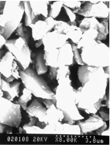
The tool, Cu/SiCp composite electrode, was of cylin-drical and flat-ended shape with a diameter of 8 mm and fabricated by the powder metallurgy method. The copper powder was of dendritic shape with a particle size range of 20–40 µm; the SiCp powders assumed an irregular polygonal shape with sharp angles (Fig. 3) with 3, 63, 150, and 250 µm mean sizes were used for reinforce-ment.
In order to obtain optimal bonding between the SiCp and Cu matrix through a completely continuous copper film on SiCp, the following electroless plating steps were applied:
1. Surface treatment: surface cleaning of SiCp was
Fig. 3. The SiCppowders with irregular polygonal shape.
accomplished by immersing in acetone under ultra-sonic vibration for 30 min. After rinsing with de-ion-ized water, SiCpwas heated at 600°C for 3 h in an air drying oven and were subsequently ground to break agglomerated particles.
2. Sensitizing and activating: the cleaned SiCpwere sen-sitized in a solution containing stannous chloride (SnCl2·2H2O) and hydrochloric acid (HCl) for an hour and then activated in a solution containing palladium chloride (PdCl2) and hydrochloric acid for an hour. 3. Electroless copper plating process: the cleaned and
activated SiCp (60 g/l) were placed separately into CuSO4·5H2O (20 g/l) and KNaC4H4O6 (50 g/l) sol-utions, ultrasonically shaken, followed with continu-ous stirring during mixing of the two solutions. Then, HCOH (36%) solution was added to the mixed sol-ution. The pH of the solution was subsequently adjusted by adding NaOH to pH 13; at this stage, cop-per started to plate onto SiCp surface.
Copper powders with 0 and 20 wt% SiC powder were mixed well and cold formed by pressing at 450 MPa pressure. A series of compacts were heated to 800 °C for 8 h in nitrogen. In the EDMG operation, only those grains with a protrusion height greater than the gap width between the workpiece and electrode can physically interact with the workpiece. Therefore, the working sur-face of sintered compact is etched by HNO3 for 2 min before EDMG operation in order to create many quali-fied protrusions. In Fig. 4, it can be seen that the grains protrude from the copper matrix, and with these pro-trusions the grinding function can be brought into effect. An experiment was conducted to investigate the effect of SiCpparticle sizes and the rotating speed of the elec-trodes on the EDMG performance of mold steel having a diameter of 12 mm with a 4 mm hole through the center, and the chemical composition of the steel is as shown in Table 2.
The dielectric fluid used in these experiments was Castrol SPE oil having a hydrocarbon base with a kine-matic viscosity of 2.08 cSt at 40 °C.
Table 2
The chemical composition of HPM50 mold steel
Element C Si Mn Ni Al Cu Mo Fe
wt% 0.05–0.18 0.15–1.0 1.0–2.0 2.5–3.5 0.5–1.5 0.7–1.5 0.1–0.4 Balance The front gap width between electrode and workpiece
was measured through the following ways:
1. The electrode attached on machine head was moved to contact with workpiece before EDM was ignited and the dial gage on EDM machine head was set at zero.
2. Raised the electrode, set the working current, then ignited EDM starting switch, the electrode would be moved toward workpiece by servo mechanism. 3. The value showed on dial gage, when first series of
spark ignited between electrode and workpiece, gave the front gap width at the set working current.
3. Results and discussion
3.1. Effect of discharge current on EDM
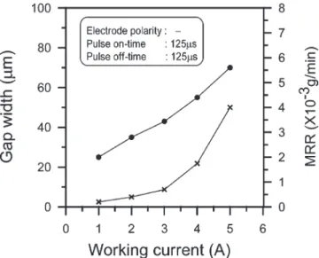
EDM machining performance is controlled mainly by the front spark gap between electrode and workpiece. Preliminary experiments indicated that the machining parameters such as the discharge current, breakdown voltage, pulse duration, dielectric strength and electrode polarity have obvious effects on the machining of mold steel. For the sake of simplification, only the discharge current factor was selected to change the front spark gap width. Numerous current values were chosen for the experiments while other machining parameters were fixed. Three measurements were taken at each current and the average values were adopted. Fig. 5shows the
Fig. 5. Effect of current on gap width and MRR using copper elec-trode.
effect of varying discharge current on the front spark gap width with an electrolytic copper electrode containing 0 wt% SiCp.
The results indicate that the front gap width increases as the current increases, and their relationship for 250
µs pulse duration approaches the following equation Gap width (µm)⫽ 11 A ⫹ 12.6 (1) where A is the working current.
Material removal rate is one of the important para-meters for evaluating the EDM machining performance for a particular working setup.Fig. 5also shows the vari-ation of current vs. MRR. The results also indicate that the MRR increases as the current increases and their relationship approaches the following equation
MRR⫽ e0.659 A⫺2.077 (2)
As yet, no expression has been depicted that can pre-dict fully the rate of metal removal in EDM. This rate depends on a large number of properties of the work-piece material, including its melting point, thermal con-ductivity and latent heat. It is also influenced by the properties of the electrodes, and by the geometric factors such as the shape and the dimensions of electrode and workpiece.
An ideal EDM tool electrode should not only be cap-able of removing the maximum amount of material from the workpiece, but also of resisting self-erosion. During EDM, material removed from electrode (⌬er) consists of three forms, i.e. forms of vapor (⌬v), liquid (⌬l) and solid particles produced as a result of brittle rupture of the electrode (⌬s) [29], i.e.
⌬er ⫽ ⌬v ⫹ ⌬l ⫹ ⌬s (3)
⌬v and ⌬l depend on the boiling and melting point,
respectively of the electrode material, while⌬s is a func-tion of electrode mechanical strength. As the bonding strength of the electrode increases, ⌬s reduces and ⌬v + ⌬l constitutes the major part of ⌬er.
Fig. 6 shows the effect of working current on elec-trode wear ratio, i.e. the ratio of elecelec-trode loss over workpiece loss. An increase in current is always accompanied by an increase in the electrode wear ratio. This is due to the fact that higher current densities gener-ate large amounts of heat, which rapidly overheats the electrode and causes it to wear.
Fig. 6. Effect of current on electrode wear ratio. 3.2. Effect of electroless copper plating on electrode strength
When the grinding function was introduced in the EDMG operation, an electrode with good bonding between SiCp and copper can prevent the SiCp particle from peeling off the copper matrix. The electroless plat-ing process was recognized as havplat-ing a tremendous effect on the tensile property of copper matrix composite
[30]. Fig. 7 shows the variation of tensile strength vs.
Fig. 7. Effect of particle size on tensile stress of sintered Cu/SiC composite.
SiCpparticle size, demonstrating that the tensile strength of composites using uncoated SiCp is lower than that of composites with electroless copper plated SiCp. The strength of the composite decreases as the SiCpparticle size increases. With a very small particle size, such as those smaller than 5 µm, the dispersion strengthening mechanism was brought into effect and a maximum ten-sile stress appeared. As particle size increased, the strength of the composite is reduced by the presence of more defects between the copper matrix and SiCp par-ticle.
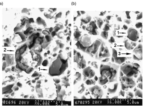
SEM micrographs of the fracture surface of the com-posite with 3µm 20 wt% non-coated SiCp are shown in
Fig. 8(a), in which arrow 1 indicates the decohesion of the SiCp/Cu interface, and arrow 2 indicates SiCp cracked by pressing or tensile test; all SiCp show rela-tively flat surfaces of row SiCppowder shape, and these phenomena show the poor Cu/SiCp interface bonding status. The fracture surface of the composite with 3µm 20 wt% coated SiCp is shown in Fig. 8(b), in which arrow 1 indicates SiCp with copper film still covered appearance at the dimple bottom, and arrows 2 and 3 indicate good bonding status between Cu and SiCp, the copper film on the SiCp surface is still observed on the fracture surface. In both samples, fracture appears to initiate at the SiCp particles, with the fracture surfaces characterized by the presence of large microvoids with SiCp particles seated at the center of each dimple. The crack may propagate along the interface between SiCp particles and matrix, and within SiCp particles. Besides the normal ductile dimple fracture of the matrix, there are two types of fracture behavior related with SiCp; namely, fracture of SiCpand decohesion of the SiCp/Cu interface. In Fig. 8(a), the fracture surface shows the presence of decohesion at the SiCp/Cu interface. How-ever, the occurrence of SiCp fracture was observed in
Fig. 8(b), and this indicates that there was a load transfer from the matrix to the SiCp.
3.3. Electrical discharge machining and grinding surface
EDMed surfaces generally have a complex appear-ance covered by shallow craters, spherical particles and pockmarks formed by entrapped gases escaping from the redeposit material [31]. Spherical particles are molten metals that were expelled randomly during the discharge and later solidified attaching to the crater sides on the workpiece surface. While pockmarks look like the rem-nants of bubble evolution, the edges of some of the pock-mark are thin and sharp, suggesting the molten metal having been solidified at an extremely high rate. Typical surface structures of HPM50 mold steel surface machined by EDMG are shown in Fig. 9. In Fig. 9(a), with 63µm SiCpelectrode and 2 A working current, the estimated SiCp protrusion value is 19 µm(30% of the
Fig. 8. SEM micrographs of the fracture surface of: (a) non-coated electrode, (b) copper coated electrode.
Fig. 9. SEM micrograph showing surface morphology of mold steel EDMGed with composite electrode of various SiCpparticles size at 2250
rpm rotating speed, 125µs pulse on-time and 2 A current setting: (a) 63µm SiCp, 1 is crater, 2 is spherical particle, 3 is pock mark, (b) 250µm
SiCp, (c) 150µm SiCp.
SiCpparticle size) and the average front spark gap is 35
µm. The former is much smaller than the later. It seems that the electrical discharge grinding function has little effect on the workpiece surface, for only some shallow grinding traces were observed on the bigger spherical particles surface or higher hump of the workpiece. Besides the feature of the EDMed surface, both SiCp debris and microcracks can also be observed on the fig-ure; these cracks are formed as a result of the exceed-ingly high thermal stresses prevailing at the specimen surface as it cooled at a fast rate after the discharge.
With 250µm SiCpelectrode and 2 A working current, as shown inFig. 9(b), the estimated SiCpprotrusion is 75
µm and front spark gap between matrix and workpiece is 36 µm approximately. The SiCp protrusion passes
through the resolidified zone and penetrates into the heat affected zone, or possibly even deep into matrix. Under this EDMG condition, the MRR is attributed mainly to the grinding mechanism. Evident proof of the dominant grinding effect can be found from the grinding marks covering the whole EDMGed surface, except for some deeper crater caused by EDM mechanism.
When SiCp particle size and working current were optimally selected with 150µm SiCp electrode and 2 A working current, only the hump around the spark crater would be ground away from matrix, as shown in Fig. 9(c). The total MRR under this EDMG condition is attri-buted to both the EDM process and the hump grinding process.
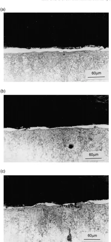
cross-Fig. 10. Optical micrograph showing the thickness of the white layer after EDMG with various SiCp sizes electrode at 2250 rpm rotating
speed, 2 A current setting, 125µs pulse on-time: (a) 63µm SiCp, (b)
150µm SiCp, (c) 250µm SiCp.
section taken from HPM50 specimens after EDMG oper-ation, in which three layers are observed: the resolidified layer, heat affected layer, and matrix. When etched with a dilute nitric acid solution, the outmost layer in these specimens remained bright and featureless, i.e. they were non-etchable. This white layer was formed when the out-ermost molten material was quenched at an extremely
high rate by flushes of the dielectric. The optical micro-graphs of Fig. 10(a) shows the white layer of the EDMGed surface with 63µm SiCpelectrode; both pock mark and microcrack are observed on this layer and no grinding trace is observed in this figure.Fig. 10(b)shows the white layer of specimens with optimum SiCpcontent and electrode rotating speed; a thin white layer after the grinding action is observed, and the ungrounded white layer has the same thickness as that of the white layer inFig. 10(a). Using an electrode with a larger SiCp par-ticle size, the white layer is pricked, and the heat affected zone is ground by SiCp directly. The result is shown clearly inFig. 10(c).
To understand the mechanism of particle size effect on EDMG, it is necessary to examine the relationship between the gap width between workpiece and electrode, thickness of the resolidfied layer and SiCp particle size. A schematic illustration of these relationships is presented in Fig. 11. The white layer thickness were measured at various points on different cross-section of the specimen EDMGed at selected current; the width was obtained by measuring the gap from electrode top surface to workpiece surface; the SiCp grains protrusion height was about 30% of the average SiCp grain size. As can be seen from Fig. 11(a), when working current was set at 1 A, the gap width between electrode and workpiece shown inFig. 5was 25µm and the resolidfied zone was 21µm, the protrusion of electrode with 63µm
Fig. 11. Schematic illustration of the relationships between particle size, gap width and thickness of resolidfied zone EDMGed with vari-ous currents: (a) 1, (b) 3, (c) 5 A.
SiCp was 19µm, which was almost in contact with the resolidfied zone, grinding function has little effect on workpiece surface, the MRR of EDMG are nearly close to the MRR of EDM using copper as electrode. The white layer would be ground by the particle protrusion of electrode with 150 µm SiCp, and the matrix was ground by the particle protrusion of electrode with 250
µm SiCp. Gap width and resolidfied zone thickness would increase with increasing working current. In Fig. 11(b) and (c), when 3 and 5 A current were set, the gap width was 43 and 70 µm, and the average resolidfied zone thickness was 23 and 25 µm, respectively. Only that the particle protrusion of electrode be able to reach the resolidfied zone can grinding action occur, i.e. the matrix would be ground at 3 A working current with 250 µm SiCp electrode and only the hump was ground at 3 A working current with 150µm SiCp electrode and 5 A working current with 250 µm SiCp electrode.
The EDMed surface roughness depends generally on both the pulse energy and current in a complex manner. By and large, at a given pulse energy, a poor surface finish is obtained with a higher pulse current. It is possible that a higher pulse current may cause more frequent cracking of the dielectric, giving rise to more frequent melt expul-sion. This in turn would result in a higher density of spherical particles and poor surface finish. In this experi-ment, the focus of attention is the difference of surface morphology between the EDMed and EDMGed surface, and not the variance of working current on surface rough-ness. From the appearance of the EDMGed surface shown inFig. 9(b) and (c), the hump and the spherical particles that protruded from the workpiece surface would be grounded first by the protruding SiCp. Undoubtedly, the surface roughness of the EDMGed surface would there-fore be finer than that of the EDMed surface. InFig. 12, it shows the surface roughnesses of HPM 50 EDMed and EDMGed surfaces. The roughnesses using electrodes with SiCp sizes of 63, 150 and 250µm are lower than that of electrode with SiCpsizes of 0 and 3µm, this is attributed to the electrode grinding function being introduced on workpiece surface. Besides, the surface roughness of EDMGed HPM 50 surface using electrode with 3 µm SiCp is higher than that of EDMed surface with 0 µm SiCp, this can be possibly explained as follows: when at same working current and working area, the electrode with 3 µm SiCp would induce higher current density on workpiece because some Cu electrode was replaced by much less conductive SiCp, allied with the concave shape of discharge arc, this leads to localized workpiece melting and vaporizing, deeper crater and higher hump are thus introduced resulting in higher surface roughness.
3.4. Effects of electrode rotating speed and working current
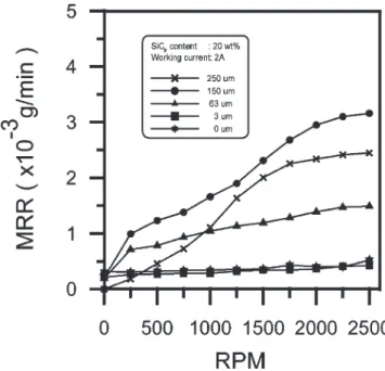
The results in Fig. 13 show the effect of electrode rotating speed on MRR with various SiCp sizes
elec-Fig. 12. The surface roughness of EDMed (with 0µm particle size) and EDMGed surfaces at 2250 rpm rotating speed, 125µs pulse on-time and 2 A working current.
Fig. 13. The effect of electrode rotating speed on MRR using elec-trodes with various SiCpsizes.
trodes at 2 A working current. It demonstrates that all of the MRRs of EDMG, using composite electrodes and at 0 rpm rotating speed, are lower than when using pure copper electrode; the MRR of EDMG approached zero when the 250 µm SiCp electrode was used. These phenomena may be explained as follows: when EDMG with composite electrode, electrode and workpiece moved to a very small gap by servomechanism, only the copper, which possesses low electric resistance on the electrode front surface, can generate spark. No sparks were induced from SiCpto workpiece for the high elec-tric resistance of SiCp. Consequently, the surface area
occupied by Cu metal on the electrode front is the major factor in determining the MRRs by EDM while using the same machining parameters. As the SiCp wt% increases in the electrode, the area occupied by Cu on the electrode front would be lessened leading to a decreased sparking area and resulting in a lower MRR. For the electrode with 250 µm SiCp, the SiCp protrusions are larger than the spark gap, therefore no spark was gener-ated between electrode and workpiece unless the pro-truded 250 µm SiCpwere crushed by moving the EDM machine head forward to form a smaller SiCpprotrusion and let a spark be generated. This is the reason why the MRR of EDMG is near zero when using 250 µm SiCp electrode at 0 rpm rotating speed.
When EDMG was performed with copper electrode or 3 µm SiCpelectrode, the MRR retained a low value, i.e. 0.3×10⫺3g / min in this experiment, despite the elec-trode rotating speed being gradually increased. This is attributed to the fact that no grinding action happened between the electrode and workpiece since nil SiCp pro-trusion can grind the workpiece surface, or the SiCp pro-trusions are too short to grind the workpiece surface. The MRRs under this machining condition were dominated by the EDM operation. In comparison with the MRR of the copper electrode, the larger SiCp size (i.e. ⬎3 µm) electrodes exhibited far lower MRRs than did the copper electrode. It also can be observed that the MRR of EDMG with 3µm SiCp electrode is slightly lower than that of the copper electrode. This phenomenon complies well with the EDMG mechanism.
When EDMG uses a 63µm SiCpelectrode, the MRR of EDMG increases steadily as electrode rotating speed increases, since grinding operation is introduced and only the top height of EDM surface was grounded away (as shown inFig. 11). The MRR increment can be attri-buted to that more material being grounded away by the SiCpas electrode rotating speed increases. When EDMG uses a 150µm SiCpelectrode, the MRR of EDMG also increases steadily from 0 to 1250 rpm electrode rotating speed range. The MRR values are higher than that of 63µm SiCpelectrode, for more SiCpprotrusion enables attacking the resolidified layer. But it is interesting to note that when the electrode rotating speed is over 1250 rpm, the MRR of EDMG increased dramatically and lev-eled off after 2250 rpm. This is attributed to the fact that under this high rotating speed condition the unsolidified layer had the duration (or the possibility) to encounter the protruded SiCp and was grounded away by SiCp, leading to much higher MRR values.
When EDMG with 250µm SiCp electrode was used, the MRR increased with higher electrode rotating speed from 0 to 1000 rpm. In this stage, only the grinding func-tion was performed, for the SiCp protrusions were far greater than the spark gap. The MRR was attributed to the grinding action and increased with higher electrode rotating speed. However, in practice, the SiCp
pro-trusions would be pressed ahead and become smaller after crushing with the workpiece by the EDM machine head’s servo movement; the smaller crushed SiCpwould grind the resolidfied layer. Consequently, the MRR increments are also observed from 1000 to 1750 rpm. When the rotating speed exceeds 1750 rpm, the MRR increments tend to level off. The MRR of EDMG are still lower than that with 150 µm SiCp electrode. From the above results, it is suggested that the EDMG process can be achieved only under optimum condition of choos-ing SiCp size, electrode speed and workchoos-ing current.
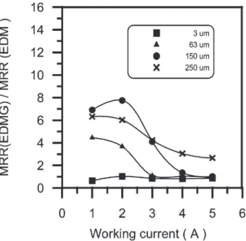
Fig. 14shows the specific value of MRR, i.e. the ratio of MRR (EDMG)/MRR (EDM), using various SiCp par-ticle size electrodes and working currents. When opti-mum machining parameters are selected (which in the present study are 2250 rpm electrode rotating speed, 2 A working current and 150 µm SiCp electrode), it was found that as high as seven times the normal EDM MRR could be achieved in EDMG operation. Allied with the expected fine surface roughness in EDMG than EDM processes (as described in the last paragraph of Section 3.3), the EDMG appears a much better processing choice than EDM.
4. Conclusions
A theoretical and experimental study on EDMG has been carried out. From the experiments and research described above, the following conclusions are drawn: 1. The combination of grinding and electrical discharge
machining could be performed by using an electrode
Fig. 14. The specific value of MRR of EDM and EDMG at different SiCpand working currents with 2250 rpm electrode rotating speed.
rotating facility and metal matrix composite electrode made by the powder metallurgy method. The com-bined machining is simple in principle, with good MRR, lower surface roughness and low equipment cost.
2. EDMG can obtain high MRR while suitable electrode rotating speed, SiCp particle size and current are chosen. When the electrode rotating speed is high enough to let hump be ground away before resolidifi-cation, much higher MRR can be achieved. The MRR can also be improved as the protrusion height of SiCp is near the sum of the gap width and white layer thick-ness.
3. Experimental results showed that the EDMG machin-ing efficiency is three to seven times that of normal EDM operation. In addition, the corresponding sur-face roughness of workpiece after EDMG operation is lower than that after EDM operation, this was also caused by the grinding function introduced in EDMG operation on workpiece surface.
Acknowledgements
The authors thank gratefully the financial support of the project by National Science Council of Taiwan under grant number NSC-89-2212-E-150-009.
References
[1] J.A. McGeough, A. De Silva, H.A. Senbel, S.C. Lee, J.Y. Wang, Proc. 13th ISEM, CIRP 1 (2001) 327.
[2] J.A. McGeough, A.B. Khayry, W. Munro, J.R. Crookall, Ann. CIRP 32 (1) (1983) 113.
[3] A.B. Khayry, J.A. McGeough, Ann. CIRP 39 (1) (1990) 191.
[4] K.P. Rajurkar, D. Zhu, J.A. McGeough, J. Kozak, A. De Silva, Ann. CIRP 48 (2) (1999) 567.
[5] G.F. Benedict, Non-traditional Manufacturing Processes, Marcel Dekker Inc., New York, 1987.
[6] S. Koshimizu, I. Inasaki, J. Mech. Work. Technol. 17 (1988) 333. [7] T. Uematsu, K. Suzuki, T. Yanase, T. Nakagawa, in: International Symposium on Mach. of Adv. Ceram. Mater. and Comp., ASME, New York, 1988, p. 135.
[8] V.S.R. Murti, P.K. Philip, Int. J. Prod. Res. 25 (2) (1987) 259. [9] J. Zhixin, Z. Jianhua, A. Xing, Int. J. Mach. Tools Manufact. 37
(2) (1997) 193.
[10] Y.C. Lin, B.H. Yan, Y.S. Chang, J. Mater. Process. Technol. 104 (2000) 171.
[11] E.Y. Grodzinskii, Mach. Tooling 50 (1979) 10. [12] V.B. Vitlin, Sov. Eng. Res. 1 (5) (1981) 88.
[13] E.Y. Grodzinskii, L.S. Zubotava, Sov. Eng. Res. 2 (3) (1982) 90. [14] S.A. Bakhuarov, Stanki Inst. 60 (1989) 18.
[15] P.C. Pandey, S.T. Jilani, Prec. Eng. 8 (2) (1986) 104. [16] H.K. Lloyd, R.H. Warren, J. Iron Steel Inst. 203 (1965) 238. [17] N.W. Bloosom, D.B. Brimhali, Mater. and Proc. Report, 1991,
26 pp.
[18] G.C. Tu, M.S. Chuang, F.M. Wang, in: Sinte. and Mater. Proce. Sixth International Symposium on the Science and Technology of Sintering, Haikou, 1995, p. 504.
[19] Metals Handbook, vol. 7, ninth ed., ASM, Metals Park, Ohio 1984, 710 pp.
[20] H. Sun, H.G. Wheat, J. Mater. Sci. 28 (1993) 5435. [21] Y.S. Chang, S.J. Lin, Scr. Mater. 35 (2) (1996) 225. [22] K.M. Zwisky, N.J. Grant, Metal Prog. (1961) 209.
[23] E.T. Denisenko, A. Polushko, N.A. Filatova, Porosh Kovaya Met. 10 (1971) 49.
[24] M.K. Surappa, P.K. Rohatgi, Metals Technol. 5 (10) (1978) 358. [25] J.H. Grimes, K.T. Scott, Powder Metall. 11 (22) (1968) 213. [26] J.A. Rogers, D.E. Miles, B.E. Hopkins, Powder Metall. 16
(1973) 66.
[27] K.F. Kobayashi, N. Tachibana, P.H. Shingu, J. Mater. Sci. 25 (7) (1990) 3149.
[28] P. Koshy, V.K. Jain, G.K. Lal, Int. J. Mach. Tools Manufact. 36 (10) (1996) 1173.
[29] M.P. Samuel, P.K. Philip, Int. J. Mach. Tools Manufact. 37 (11) (1997) 1625.
[30] Y.F. Lee, S.L. Lee, C.L. Chuang, J.C. Lin, Powder Metall. 42 (2) (1999) 147.
[31] L.C. Lee, L.C. Lin, V. Narayanan, V.C. Venkatesh, Int. J. Mach. Tools Manufact. 28 (4) (1988) 359.