2220 IEEE TRANSACTIONS ON ANTENNAS AND PROPAGATION, VOL. 53, NO. 7, JULY 2005
Studies of Suppression of the Reflected Wave and
Beam-Scanning Features of the Antenna Arrays
I-Yu Chen, Chien-Jen Wang, Hua-Lin Guan, and Christina F. Jou
Abstract—This paper describes a two-directional linear scanned design by integrating a short leaky-wave antenna (LWA) with aper-ture-coupled patch antenna arrays. This architecture proposes a technique not only having the advantage of suppressing the back-lobe due to the reflected wave in the short LWA but also producing two separate linearly scanned beams, each of them radiating in a different region of space (in both the front side and backside of the LWA). In this design, most of the reflected wave of the short LWA is coupled to the patch antenna arrays on the backside of the substrate. The phase of this coupled signal to each antenna ele-ment is adjusted by tuning the individual phase shifter in order to control electronically the patch antenna main beam in the cross plane ( 0). Meanwhile, on the front side, the main beam of the short LWA can be simultaneously scanned in the elevation plane( 0) by changing the operating frequency. Hence, the two linear beam-scanning radiation patterns of individual direc-tion can be created independently, including a narrow beam in the elevation plane ( plane at 0) at the front side and a broadside beam in the cross plane ( plane at 0) on the backside. The measured results show that the reflected wave of the short LWA in the proposed design is suppressed 8 dB as com-pared with a traditional short LWA without the aperture-coupled antenna arrays at 10.5 GHz. As a result, this novel architecture provides more flexibility both in the upward elevation plane (H plane) and the downward cross plane (backside-E plane) for pos-sible beam-scanning applications in microwave communications and remote identification.
Index Terms—Aperture-coupled patch antenna arrays, phase shifter, reflected wave, varactor diode.
I. INTRODUCTION
T
HE conventional microstrip leaky-wave antenna (LWA) has the characteristics of wide bandwidth, narrow beam, and frequency scanning capability [1]–[4]. Although the leaky-wave antenna has an excellent beam-scanning ability, the se-rious problem of the leaky-wave antenna lies in structures of huge size and long length. Hence, there has been a lot of re-search devoted to studying this issue with the hope to reduce the LWA length in order to make the use of LWAs more exten-sively [1], [5], [6]. In [1], it was mentioned that with a strip of 10.0 cm , the leaky-wave antenna could radiate about 65% of the power. The remaining power was reflected from the open end of the antenna and produced a large back lobe from the same angle in the broadside direction. If the antenna strip length Manuscript received February 26, 2004; revised December 10, 2004. This work was supported by the National Science Council of Taiwan, R.O.C., under the Grants NSC 90-2213-E-035-035 and 90-2213-E-009-053.I.-Y. Chen, H.-L. Guan, and C. F. Jou are with the Department of Communi-cation Engineering, National Chiao-Tung University, Hsinchu, Taiwan, R.O.C. C.-J. Wang is with the Department of Electrical Engineering, Feng Chia Uni-versity, Taichung, Taiwan, R.O.C.
Digital Object Identifier 10.1109/TAP.2005.850713
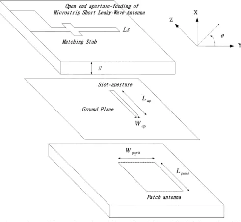
Fig. 1. Configuration of the short leaky-wave antenna integrated with the 1-, 2-, and 4-element aperture-fed patch antenna arrays.
is increased to 21.7 cm , 90% of the power could be radiated out. In our previous study, we found that the reflected wave was only 3 dB lower than the main beam [5]. The reflected power resulting from the mismatch of the open end of the mi-crostrip leaky-wave antenna would cause an undesired interfer-ence in the processing of RF microwave signals. According to the recent research, it was understood that the reflected wave could be suppressed by using technologies of longer antenna length [1], or array topology [5], or a taper-loaded antenna end [6]. However, all the proposals mentioned above require large circuit size or complicated structure.
In 1979, Menzel proposed an asymmetrical feeding arrange-ment and an impedance-matching network to excite the leaky-mode of the microstrip line [1]. Also, Lin et al. [7] proposed three feeding structures for the microstrip leaky-wave antenna in 1996. These proposed structures (slotline-fed, coupled-slot-line-fed, CPS-fed) could enhance the microstrip line antenna to radiate in first higher-order mode. In 1997, Luxey and La-heurte [8] made use of an open-ended CPW slot in the center of the antenna to excite the leaky mode at C band. From the literature described above, we know that the first high order mode is successfully excited by asymmetrical feeding. Further-more, some attempts of the two-dimensional beam-scanning LWA especially in the elevation plane (the H plane) and the cross 0018-926X/$20.00 © 2005 IEEE
Fig. 2. Geometry and coordinate system for the aperture-coupled patch antenna.
plane (the quasi-E plane) have been made by encompassing the phase control technique of the coupling oscillators or by uti-lizing the 4 1 aperture-coupled series-fed electronically steer-able microstrip LWA array [9], [10].
In this paper, an alternative structure with two-directional space beam-scanning capability is proposed. This proposed array is made up of two types of antennas fed in series. One of them is a microstrip short LWA, whose scanning beams are radiated above the ground plane. The other beam-scanning antenna is a linear array of phase-controlled aperture-coupled patch antennas that radiate below the ground plane. This pro-posed novel short microstrip LWA (2 wavelengths) integrated with the aperture-coupled phase arrays is shown in Fig. 1. In this design, the back lobe of the short LWA can be suppressed effectively since the apertures transfer the remaining power from the antenna end to the patch arrays on the backside. In addition, by changing the operating frequency, the LWA has beam-scanning capability in the elevation plane ( -plane in Fig. 1) located on the half space side of leaky-wave line , and the power-combining beam of the patch arrays can scan in the cross plane ( plane) on the patch half space by utilizing the electronically tuning varactor-diode phase shifters.
II. CIRCUITDESIGN
The proposed geometry and coordinate system for the topologies of the designed LWA integrated with the aper-ture-coupled phase arrays are shown in Fig. 1. The topology of
Fig. 3. Schematic diagram of the varactor-tuned phase shifter.
the beam-scanning LWA module consists of three parts: a mi-crostrip leaky-wave antenna on the top plane, the apertures, and the patch antenna arrays on the bottom of the substrate plane. The whole circuit was designed and fabricated on RT/Duroid substrate with a dielectric constant of and a thickness
of mm. The length and the width
of the microstrip LWA are calculated to be 60 and 11 mm in such a way that the leaky mode can be excited in an operating frequency range from 9.0 to 10.5 GHz. The input feeding line of this LWA is designed to be 50 ohms characteristic impedance. The geometry of the aperture-coupled patch antenna is shown in Fig. 2. The length and the width of the patch antenna are designed to be 10 and 8 mm in order to have the best power radiation. The overlap length of the feeding line is optimized to be 2.3 mm. Each of the patch antennas is aper-ture-fed by a microstrip line with a characteristic impedance of 50 ohms and an open stub is added to the feeding line of the arrays to perform the impedance matching to reduce the mismatch due to mutual coupling. The aperture-feeding
2222 IEEE TRANSACTIONS ON ANTENNAS AND PROPAGATION, VOL. 53, NO. 7, JULY 2005
Fig. 4. Simulated and measured return loss of the short LWA with an open end.
Fig. 5. Simulated and measured return loss of the short LWA integrated with an aperture-coupled patch antenna.
structure is designed to couple the remaining power of the leaky-wave antenna into the patch antenna [11]. The length and the width of the aperture were optimized to be 3.5 and 0.5 mm. The space between the patch antenna elements is 18.4 mm.
In order to change the phase difference between the ra-diating elements, a pair of phase shifters was designed and fabricated to modulate the phase of each input signal. Fig. 3 shows the simplified schematic diagram of the varactor-tuned phase shifter proposed in [12]. The varactor-tuned phase shifter was designed from 9.0 to 10.5 GHz by using a commercially available CAD tool. Varactor-diode phase shifters are basically analog devices in which the variable reactance is achieved through voltage-tuned capacitance of the diode under the re-verse-bias condition. As the bias voltage of this GaAs varactor (M/A-COM MA46410) is varied from 0 V to a large negative value close to its breakdown voltage, V, the capacitance of the diode decreases from a maximum value to a low value , with a capacitance ratio of 10:1 and the maximum phase change can be achieved. As expected, the phase progression of the phase shifter varies linearly with bias voltage.
III. THEORETICAL ANDEXPERIMENTALRESULTS We employed a rigorous (Wiener–Hopf) solution [13] to find the normalized complex propagation constant of
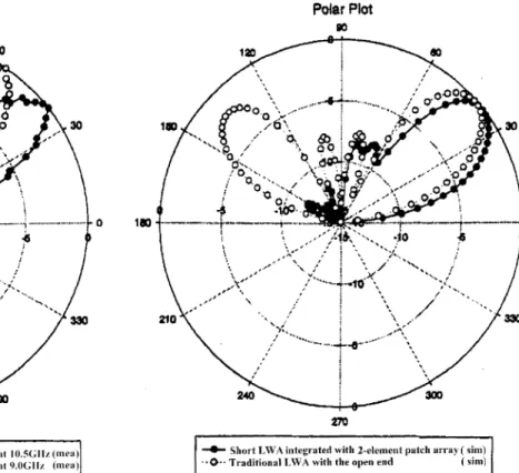
Fig. 6. Comparison of the measured H-plane radiation patterns of the proposed antenna structure comparing to the traditional LWA at 10.5 GHz.
the first higher order mode, where is the normalized phase constant and is the normalized attenuation constant. Moreover, the LWA scanning angle between the main-beam direction and the end-fire direction (the -axis direction) is calculated using the equation . Hence, the angle is a function of frequency. After comparing the results of Fig. 4 and [7], it is expected that the asymmetrical feeding would excite the first higher mode. Fig. 4 shows the simulated and measured return loss of the traditional LWA with the open end. Fig. 5 shows our simulated and measured return loss of this short LWA integrated with an aperture-coupled patch antenna. A higher frequency 10.5 GHz was chosen because of its high reflection coefficient. However, in this case, it was found that the return loss had improved by over 30 dB at 10.5 GHz when compared with traditional short LWA. This indicates that the proposed antenna configuration indeed had radiated power through the aperture to the backside. In addition, we had also found that the proposed configuration could enhance the LWA radiation efficiency and provide a broader bandwidth. Fig. 6 illustrates the measured H-plane radiation patterns of the proposed antenna structure in comparison with the traditional LWA at 10.5 GHz. The measured power of the reflected wave of the traditional LWA is only 2 dB lower than the main beam, but the proposed design can suppress the reflected wave by at least 8 dB. The measured H-plane beam-scanning radiation patterns of the proposed structure are shown in Fig. 7. It shows that as the operating frequency varies, the main beam could be steered toward the endfire electronically in the elevation plane. The main beam scans from 38 to 58 as the operating frequency increases from 9.0 to 10.5 GHz. On the back side,
Fig. 7. The measured radiation patterns of the short LWA integrated with an aperture- coupled patch antenna at 9.0 and 10.5 GHz.
Fig. 8. The simulated and measured return loss of the short LWA integrated with 2-element aperture-coupled patch antenna arrays.
the measured power density at the peak of the main beam of the single-element patch antenna at the downward E plane is 4.83 dB lower than the measured power density radiated from the upward LWA. Furthermore, the beamwidth of the patch beam is about 60 . Fig. 8 shows the simulated and measured return loss of the short LWA integrated with the two-element aperture-coupled patch arrays. The return loss is about 20 dB at 10.5 GHz. Figs. 9 and 10 illustrate the simulated and the measured H-plane beam-scanning radiation patterns between the short LWA integrated with the two-element patch antenna arrays and the traditional LWA. In the following figures we will show that as the number of patch elements increases, the backside radiation power become more comparable as the front side LWA radiation power. Fig. 11 shows simulated and
Fig. 9. Comparison of the simulated radiation patterns between the short LWA integrated with the 2-element aperture-coupled patch arrays and the traditional LWA.
Fig. 10. Comparison of the measured radiation patterns between the short LWA integrated with the 2-element aperture-coupled patch arrays and the traditional LWA.
measured backside E-plane radiation patterns of 2-element patch antenna arrays. It is found that the maximum power of
2224 IEEE TRANSACTIONS ON ANTENNAS AND PROPAGATION, VOL. 53, NO. 7, JULY 2005
Fig. 11. Simulated and measured radiation pattern of the 2-element aperture-coupled patch antenna arrays.
Fig. 12. Comparison of the measured radiation patterns between the short LWA integrated with the 4-element aperture-coupled patch arrays and the traditional LWA.
Fig. 13. Measured radiation pattern of the short LWA integrated with 2-element aperture-coupled patch arrays at the bias of015 V.
the two-element patch arrays is 2 dB less than the maximum power beam of the LWA, and the beamwidth of the patch beam is 20 . Fig. 12 shows the comparison of the measured H-plane beam-scanning radiation patterns between the proposed short antenna design with four-element aperture-coupled patch arrays and the traditional LWA. As you can see the maximum power beam of patch antenna arrays at the backside—E plane is only 1.17 dB less than the maximum power beam of the LWA; meanwhile, the beamwidth of the patch arrays is approximately 10 .
In our past experience with respect to two-element antenna arrays using delay lines, the beam directly points to the broadside direction when the phase is in phase, and if the phase difference is 45 , the beam will steer 8 at 10.5 GHz. If the phase difference is 90 , the main beam is steered 22 off the broadside. When the bias voltage of the varactor diode is changed, the phase of the output signal of the phase shifter will vary and the phase difference between each input signal of the radiating elements will be modulated. As expected, the phase progression of the phase shifter varies linearly with the bias voltage of the varactor diode. The phase varied 65 with the control voltage of 15 V and the results also proved that the matching is good between each stage. Thus, the proposed phase shifter can achieve the beam-scanning ability. Fig. 13 shows the measured backside-E plane phase-scanning patterns of the two-element phased arrays with control voltage of ( 15 V, 0 V) and (0 V, 15 V). The scanning angle of the patch beam is . The direction of the main beam can be steered from 260 to 280 , respectively. According to the scanning angle of the experimental results, it
system, or radiolocation, etc. Thus, there is great potential for application in the future.
REFERENCES
[1] W. Menzel, “A new traveling-wave antenna in microstrip,” Archiv. Elek-tronik. Ubertrag Tech., pp. 137–140, Apr. 1979. Band 33.
[2] G. J. Jou and C. C. K. Tzuang, “Oscillator-type active-integrated antenna: The leaky-mode approach,” IEEE Trans. Microwave Theory Tech., vol. 44, no. 12, pp. 2265–2272, Dec. 1996.
[3] C. Luxey and J. M. Laheurte, “Dual-beam array of microstrip leaky-wave antennas,” IEE Electron. Lett., vol. 34, no. 11, pp. 1041–1042, May 1998.
[4] C.-J. Wang, Y.-H. Sheu, and C. F. Jou, “A dual-beam asymmetrically scanning leaky-wave antenna by utilizing a HEMT resistive upcon-verter,” IEEE Microwave Wireless Components Lett., vol. 11, no. 12, pp. 492–494, Dec. 2000.
[5] C. J. Wang, C. F. Jou, J. J. Wu, and S. T. Peng, “Radiation characteristic of active frequency-scanning leaky-mode antenna arrays,” IEICE Trans. Electron., vol. E82-C, no. 7, pp. 1223–1228, Jul. 1999.
[6] Y. C. Shih, S. K. Chen, C. C. Hu, and C. F. Jou, “Active feedback mi-crostrip leaky wave antenna-synthesizer design with suppressed back lobe radiation,” IEE Electron. Lett., vol. 35, no. 7, pp. 513–514, Apr. 1999.
[7] Y.-D. Lin, J.-W. Sdheen, and C.-K. Tzuang, “Analysis and design of feeding structures of microstrip leaky-wave antenna,” IEEE Trans. An-tennas Propag., vol. 44, no. 9, pp. 1540–1547, Sep. 1996.
[8] C. Luxey and J. M. Laheurte, “Simple design of dual-beam leaky-wave antennas in microstrips,” Proc. Inst. Elect. Eng.-Microwave, Antennas, and Propagation, vol. 44, no. 6, pp. 397–401, Dec. 1997.
[9] C. C. Hu, J. J. Wu, and C. F. Jou, “A two-dimensional beam-scanning linear active leaky-wave antenna array,” IEEE Microwave Guided Wave Lett., vol. 9, pp. 102–104, Mar. 1999.
[10] C. C. Hu, C. F. Jou, and J. J. Wu, “An aperture-coupled linear microstrip leaky-wave antenna with two-dimensional dual-beam scanning capa-bility,” IEEE Trans. Antennas Propag., vol. 48, no. 6, pp. 909–913, Jun. 2000.
[11] D. M. Pozar, “A microstrip antenna aperture coupled to a microstrip line,” IEE Electron. Lett., vol. 21, pp. 49–50, Jan. 1985.
[12] R. H. Jardin, E. J. Downey, and J. Munushian, “Electronically-variable phase shifters utilizing variable capacitance diode,” Proc. IRE Lett., vol. 48, pp. 944–945, May 1960.
[13] D. C. Chang and E. F. Kuester, “Total and partial reflection from the end of a parallel-plate waveguide with an extended dielectric loading,” Radio Sci., vol. 16, pp. 1–13, Jan.–Feb. 1981.
Chien-Jen Wang was born in Kaohsiung, Taiwan,
R.O.C., in 1971. He received the B.S. degree in elec-trical engineering from the National Sun-Yet-Sen University, Kaohsiung, Taiwan, R.O.C., and the Ph.D. degree in communication engineering from the National Chiao-Tung University, Hsinchu, Taiwan, R.O.C., in 1993 and 2000, respectively.
From 2000 to 2001, he was at BENQ Corporation, Taipei, Taiwan, R.O.C., as a Project Researcher in the Wireless Communication Division, where he was re-sponsible for the antenna module. In 2001, he joined Feng-Chia University, Taichung, Taiwan, R.O.C., as an Assistant Professor of electrical engineering and was promoted to an Associate Professor in 2004. His research activities involve the design and development of RF/microwave active and passive circuits and microstrip antennas.
Dr. Wang is a Member of Phi Tau Phi.
Hua-Lin Guan was born in Taipei, Taiwan, R.O.C., in 1977. He received the
B.S. and M.S. degrees in communication engineering from the National Chiao-Tung University, Hsinchu, Taiwan, R.O.C., in 1999 and 2001, respectively.
His research interests include electromagnetic, antenna theory, and commu-nication IC design.
Christina F. Jou was born in Taipei, Taiwan, R.O.C.,
in 1957. She received the B.S., M.S., and Ph.D. degrees in electrical engineering from the University of California, Los Angeles, in 1980, 1982, 1987, respectively. The subject of her doctoral thesis was the millimeter wave monolithic Schottky diode-grid frequency doubler.
From 1987 to 1990, she worked at Hughes Air-craft Company, Torrance, CA, as a Member of the Technical Staff in the Microwave Products Division, where she was responsible for microwave device modeling. In 1990, she joined National Chiao-Tung University, Hsinchu, Taiwan, R.O.C., where she is now an Associate Professor of communication engineering. Her current research is in developing RF and microwave active circuits and MEM antennas, and filter.