10.00 CTuD6
AlCSmirnodudor Miniitore Nonlinear Optical L m p Mirrors for Wiz AU-Optical Switching Operation
Jiun-Haw
Lee,
Chih-Yang Wang, Yean-Woei Kiang, andL L Y a n g
Deparlment of Electrical Engineering, G d u & InStible of Elcctro-Optieal Engineering, and Graduate Institute ofCommunication Engineering, National Taiwan Ilniversity,
1, Ruosevell Road, Sec. 4, Taipei. Taiwan,
R.O.C.
(phonc) 886-2-23657624 (fax) 886-2-23652637 (E-mail)Conventionally, B nonlinear interfemmcta consists of an optical fiber loop, connsled with a fiber coupler. In this paper, we report our experimental re~ults of a monolithic all-semiconduetor-oplical-amplifier nonlinear optical loop dcvice with psee signals. Thr: device includes il circular loop, a multi-mode inlerfcrencc wavcguidc amplifier (MMIWA, acting as a nonlinear coupler). and inputfoulput porn [I]. All parts of the dcviee arc made of GaAriAIGa/\s ridge waveguide semiconductor optical ampliticra. Thc clrctm- pad is divided into row disconneclcd regions b provide p i n %parately Panicularly, the loop
IS dividcd into two different injection areas to make the loop asymmetric. In OUT experimcntv, wc uscd the pulsed signals with a pulse width o f I . 4 pscc.
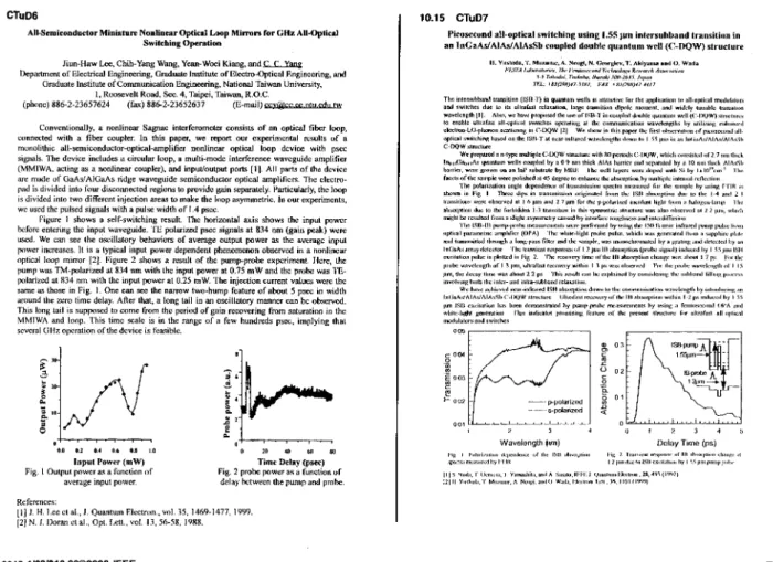
Figure I shows a self-switching rcsult. I'he horizontal axis shows thc inpul powr before entering the input wavsguide.
'IB
polarized p y c signals at 834 nm (gain peak) wereu%d. We m see the oscillatory behaviors o f average output power as the w e q c input power increases. I1 is a lypical input power dependent phenamcnon obxrvod i n a nonlinear opticai loop mirror [Z]. Figure 2 shows a result o f thc pumppmbe experiment. litre, the pump was TM-polarized ill 834 nm with the input power at 0.75 mW and thc pmbe was 7 8 - polarked at 834 nm wilh the input pawer a1 0.25 mW. 'The injection cumnt values werc the same ils those in Fig. I. One can sec the n m w two-hump realwe o f about 5 psec in width nmund lhr zero lime delay. AAer that, a long lail in an oscillatory manner can be observed. This lnng tail is supposed In come fmm thc period o f gain recovering from saturation in the MMIWA and loop. This time salt is in the range of a few hundreds paec, implying thaL scvcrd Gliz opcration ofthe device is fcsiblc.
0.0 0.1 0.4 0.6 0 1 la Input Parer (GlW) Fig. I Output power BI a function of
avcrap input powcr.
0 2" &" UI I Time Dday (psec) Fig. 2 prohe powcr ar a funclion " I
delay hetween the pump and p m k . Rercrences:
[I] I. H . I r c c l a l . , I . Q u a n t u m E l e c t r r ~ n . . u o l . ~ 5 , 1469-1471, I V Y 9 [Z] N. 1. Doran c l al., Opt. Lelt., vol. 13. 56-58. 1'188.
10.15
CTuD7
Picosecond all-optical switching using
1.5spm Intersuhband transiliain in
an InCaAs/AIAs/AlAsSb coupled dnuhlc quantum well (C-DQW) struelure1 3 I I , 1 1 3 4 : ,
Wavelength (M) Delay Time (ps)