A SCALABLE REED-SOLOMON DECODING PROCESSOR BASED ON
UNIFIED FINITE-FIELD PROCESSING ELEMENT DESIGN
Jih-Chiang Yeo, Huai-Yi Hsu, An-Yeu (Andy) Wu
Graduate Institute of Electronic Engineering
and Department of Electrical Engineering,
National Taiwan University, Taipei 106, Taiwan
ABSTRACTReed-Solomon (RS) codes play an important role in
providing error protection and data integrity. Many researches of RS decoder are implemented in parallel architecture, which can perform the highest data throughput rate in all RS decoder architectures. However, for some specifications such as Digital Video
Broadcasting system (DVB), the requirement of data
throughput rate is very low and a low-power folding architecture is enough to achieve the data throughput rate requirement. The hardware cost of folding architecture is also comparably much smaller than the hardware cost of parallel architecture. In this paper we present a design of a scalable RS codec processor design with a reconfigurable architecture. The reconfigurable architecture has good flexibility for tradeoff between the data throughput rate and power consumption. Compared with the DSP type architecture, the proposed reconfigurable architecture can perform higher data throughput rate with shorter latency. Besides, with combination of two RS processor engines, we can easily double the performance with the scalable design. This good scalability is another advantage of our proposed reconfigurable architecture.
1. INTRODUCTION
Reed-Solomon codec is a widely used Forward Error
Correcting (FEC) technique [1]. RS codec has good error
correction capability for burst errors. Many applications have employ RS codec, such as digital audio and video, computer memory storage, magnetic and optical recording, wireless mobile and satellite communications, cable modem and xDSL [2].
The block diagram of RS decoder is shown in Fig. 1. Many ASIC designs of hardware implementation use a parallel architecture with pipelined data paths to achieve a very high data throughput rate [3][4]. However, the hardware cost is very large for a parallel architecture. For some specifications, the requirement of data throughput
rate is very low, for example, the DVB system [5]. Recently, there are some researches of RS decoder design employing a DSP core combined with a hardware array of fine-grain processing elements [6][7][8]. The DSP type architecture provides a lower data throughput rate with a smaller hardware area, but it needs to use a DSP to maintain the control of procedures of data processing.
In this paper, we investigate in details the methodologies of the RS decoding procedure, and design a coarse-grain unified finite-field processing element. Then, based on this coarse-grained processing element, we can simplify the complexity of control and replace the DSP core circuit with only a very small control circuit.
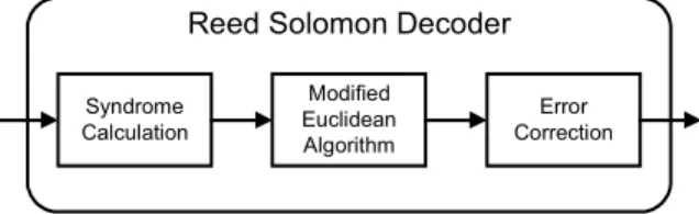
Syndrome Calculation Modified Euclidean Algorithm Error Correction
Reed Solomon Decoder
Fig. 1. Block diagram of a Reed-Solomon decoder.
2. UNIFIED FINITE-FIELD PROCESSING ELEMENT
There are three major DSP operations in the RS decoder, syndrome calculation, key equation solving, and error correction. In this section, we will analyze the common features of those DSP operations, and define the unified finite-field processing element.
2.1. Syndrome Calculation
The syndrome calculation module receives codes from channel, denoted as r(x), and calculates syndrome polynomial S(x). 2 1 0 ( ) , t i i i S x S x − = =
¦
(1)where t is the error correcting capability. Then, the coefficients of syndrome polynomial can be calculated by
148
1 0 ( ) , 0,1, ..., (2 1), n i ij i j j S r
α
rα
i t − = = =¦
= − (2)where n is the code length andө0, ө1,…, ө2t-1 are the roots of the generation polynomial in encoding. The Eq.(2) can be represented in a recursive format as
1 2 3 0
( i) (...(( i ) i )...) i ,
i n n n
S =r
α
= r−α
+r−α
+r−α
+r (3)and each iteration only needs a finite-field multiplication and a finite-field addition. The processing unit of syndrome calculation module is shown below.
Received Code
In Out
i
α
Fig. 2. Processing unit of syndrome calculation.
2.2. Modified Euclidean Algorithm
The key equation-solving module is the critical part of the RS decoder. We use the modified Euclidean algorithm to solve the key equation [9]. The key equation is
2
( ) ( ) ( ) mod( t).
S x
σ
x =ω
x x (4)where Ӻ(x) is the error location polynomial and Ԁ(x) is
the error magnitude polynomial. The modified Euclidean algorithm can be explained by following iteration descriptions. A. Initial Conditions 2 0 0 ( ) ( ) ( ) t R x x Q x S x = ° ® = °¯ , 0 0 ( ) 0 ( ) 1 L x U x = ® = ¯ (5)
B. Update Equations in Each Iteration
1 1 1 1 1 1 1 1 ( ) ( ) ( ) ( ) ( ) ( ) ( ) ( ) i l i i i i i i i i i b R x a Q x R x s x a Q x b R x Q x Q x s R x − − − − − − − − §ª º ª º· = + ° ¨« » « »¸ ¬ ¼ ¬ ¼ ° © ¹ ® §ª º· ° = ¨« »¸ ° ¬ ¼ © ¹ ¯ (6) 1 1 1 1 1 1 1 1 ( ) ( ) ( ) ( ) ( ) ( ) ( ) ( ) i l i i i i i i i i i b L x a U x L x s x a U x b L x U x U x s L x − − − − − − − − §ª º ª º· = + ° ¨« » « »¸ ¬ ¼ ¬ ¼ ° © ¹ ® §ª º· ° = ¨« »¸ ° ¬ ¼ © ¹ ¯ (7) [ ] [ ] 1 1 1 1 1 1 d e g ( ( ) ) d e g ( ( ) ) 1 0 0 . 0 1 0 . i i i i i i l R x Q x i f l s i f l − − − − − − = − ° ≥ ® = ®° ° < °¯ ¯ (8) C. Stop Condition 1 deg(Ri− ( ))x <t (9) D. Output Assignments 1 1 ( )x Qi ( ), x ( )x Ui ( )x ω = − σ = − (10)
where “a” is the highest degree coefficient of R(x), and “b” is the highest degree coefficient of Q(x). Each iteration needs four finite-field multiplication operations and two finite-field addition operations. The processing unit of key equation-solving module is shown in Fig. 3.
b a
In (R) In (Q) In (L) In (U)
Out (R) Out (Q) Out (L) Out (U)
a
b
Fig. 3. Processing unit of solving key equation.
2.3. Error Correction
The error correction module finds the locations of errors by check ifӺ(ө-k) = 0, from k = 0 to k = (n-1). This is called the Chien’s search. Chien’s search evaluates
0 ( ) ( ) , 0 , 1, ... , ( 1) . v k i k i i k n σ α− σ α − = =
¦
⋅ = − (11)Forney algorithm is used for calculating the error values. If there are some errors at the coefficient rk in the received code polynomial r(x), the error value at rk can be calculated by 1 2 1 0 1 2 1 1 3 1 3 ( ) ( ) ... ( ) ( ) ( ) ... ( ) k k t k t k k v k v error ω ω α ω α ω α σ α σ α σ α − − − + − − − − + + + + = + + (12)
Eq.(11) and Eq.(12) need a finite-field multiplication and a finite-field addition for each iteration. The processing unit of error correction module is shown below.
Summation Input
In Out
j
α
Fig. 4. Processing unit of error correction.
2.4. Unified Finite-Field Processing Element
Based on the results above, we introduce a unified finite-field processing element (PE) as shown in Fig. 5, which takes the advantage that all of the three procedures can be done at the same time. Oppositely, for a DSP type RS decoder, there is only a single procedure can be done each time, and the DSP core is needed to maintain the complex control. b a Received Code In Out summation Input In Out In (R) In (Q) In (L) In (U)
Out (R) Out (Q) Out (L) Out (U)
Modified Euclidean Algorithm
Syndrome Calculation Error Correction
i
α αj
a b
Fig. 5. Hardware architecture of the unified finite-field
processing element
3. SCALABLE DESIGN OF RECONFIGURABLE RS DEODING PROCESSOR
3.1. Proposed Reconfigurable Architecture
Since a parallel architecture takes large area and dynamic power consumption, it is not suitable for low data throughput rate specifications. And a DSP type architecture needs a DSP core circuit to maintain the complex control. A reconfigurable architecture may be a good solution because it can be reconfigured to operate at a low power mode, and doesn’t need a complex controller.
Assume that the number of processing elements is m. Fig. 6 shows our proposed architecture of reconfigurable
m-PE RS decoder design. We split all the data registers
into m segments, and each of them consists of 2t/m data registers. For each data register segment, we assign one PE to be responsible for all the operations performed on this data register segment.
4 to 1 MUX 4 to 1 MUX 4 to 1 MUX
reg reg reg reg reg reg reg reg reg reg reg reg reg reg reg reg
PE 0 PE 1 PE 2 PE 3 4 to 1 MUX 1 to 4 DeMUX 1 to 4 DeMUX 1 to 4 DeMUX 1 to 4 DeMUX
Fig. 6. Proposed scalable architecture of reconfigurable
m-PE RS decoder design. (t = 8, m = 4 example) When the data throughput rate requirement of the system specification is very low, our proposed scalable reconfigurable m-PE RS decoder can operates in single-PE mode that takes low power consumption and performs the same data throughput rate with the 2t-folding RS decoder. When the data throughput rate requirement becomes higher, our proposed scalable m-PE RS decoder can switch to a more PEs mode to satisfy the system specification.
While in single-PE mode, as shown in Fig. 7, each time there is only one PE on operating when other PEs idle without power dissipation. However, every PE needs to operate 2t/m times, for processing its own 2t/m data registers. In details, PE0 processes reg0, reg1, reg2 and reg3 separately at time slot 0, 1, 2 and 3, then the PE0 idles at time slot 4 to 15. Similarly, PE1 processes reg4, reg5, reg6 and reg7 at time slot 4 to 7, and idles at other time slots. PE2 uses time slot 8 to 11 to work, and PE3
uses time slot 12 to 15 to work. The decoder spends 2t time slots (clock cycles) for completing each iteration.
reg0 reg1 reg2 reg3 idle
reg4 reg5 reg6 reg7
reg8 reg9reg10reg11 reg12reg13reg14reg15 idle idle idle idle idle 0 1 2 3 4 5 6 7 8 9 10 11 12 13 14 15 PE0 PE1 PE2 PE3 Time
Fig. 7. Timing diagram of m-PE RS decoder in 1PE mode
for low power consumption (t = 8, m = 4 example). While in 2-PE mode, each time there are only two PEs on operating. And every PE still needs to operate 2t/m times for processing its own 2t/m data registers. The decoder spends t time slots for completing each iteration, which are half of 1PE mode, as shown in Fig. 8. Other cases are similar to these. No matter in what mode, every PE always operates 2t/m times for processing its own 2t/m data registers.
reg0 reg1 reg2 reg3
reg4 reg5 reg6 reg7
reg8 reg9reg10reg11 reg12reg13reg14reg15 idle idle 0 1 2 3 4 5 6 7 0 1 2 3 4 5 6 7 PE0 PE1 PE2 PE3 Time idle reg8 reg9reg10reg11
reg0 reg1 reg2 reg3
idle
idle reg12reg13reg14reg15 idle
reg4 reg5 reg6 reg7
idle
idle
Fig. 8. Timing diagram of m-PE RS decoder in 2PE mode
(t = 8, m = 4 example).
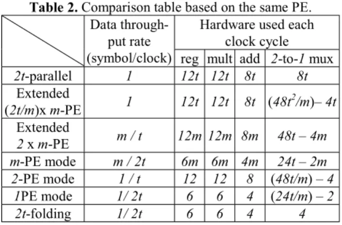
As the result, each PE needs a (2t/m)-to-1 symbol-wise multiplexer to choose from the 2t/m register data inputs, and outputs through a 1-to-(2t/m) de-multiplexer to its own 2t/m data registers. Besides, the control circuit, which generates data path control signals is just a counter, and no DSP cores are needed. The total delay on data path control is (log2t - log2m + 2) 2-to-1 multiplexers delay. The total data path control area is (24t– 6m) symbol-wise multiplexers.
3.2. Scalability
When the data throughput rate requirement is too high, and the m-PE RS decoder cannot achieve the system specification even with PE mode, we can extend the m-PE RS decoder by combining two or more the m-m-PE RS decoder to form a 2 x m-PE or higher mode RS decoder. Fig. 9 is an example of two 4-PE RS decoder combine together forming a 2 x 4-PE RS decoder. Fig. 10 shows an example of four 4-PE RS decoder combine together forming a 4 x 4-PE RS decoder, which performs the same data throughput rate with 2t-parallel RS decoder when t =
8.
4PEs RS Decoder 4 to 1 MUX 4 to 1 MUX 4 to 1 MUX
regregreg reg reg reg reg reg regregregreg regregregreg
P E 0 P E 1 P E 2 P E 3 4 to 1 MUX 1 to 4 DeMUX 1 to 4 DeMUX 1 to 4 DeMUX 1 to 4 DeMUX 4PEs RS Decoder 4 to 1 MUX 4 to 1 MUX 4 to 1 MUX
regreg reg reg reg reg regreg regregregreg regregregreg
P E 0 P E 1 P E 2 P E 3 4 to 1 MUX 1 to 4 DeMUX 1 to 4 DeMUX 1 to 4 DeMUX 1 to 4 DeMUX
Fig. 9. Extended 2 x 4-PE RS decoder
4PEs RS Decoder 4PEs RS Decoder 4PEs RS Decoder 4PEs RS Decoder
Fig. 10. Extended 4 x 4-PE RS decoder
4. PERFORMANCE COMPARISON
By using a 16-parallel architecture with our proposed PEs, we can use less gate counts to achieve 1 symbol/clock data throughput rate, which is the same with Lee’s 16-parallel architecture design [3]. Besides, with a scalable reconfigurable architecture for four PEs design, our 4-PE scalable RS decoder still has good performance, with 0.25 symbol/clock data throughput rate, compared with the DSP type architectures [6][7][8]. The comparison table is shown in Table 1.
Table 1. Comparison with other architectures (t = 8).
Area (gate) Latency (clock) Data through-put rate (symbol/clock) Lee’s 16-parallel [3] 55210 n + 66 1 16-parallel with proposed PEs 35001 n + 16 1 Proposed scalable in 4-PE mode 21526 4n + 64 0.25 Lee’s DSP [6] N/A 4n + 114 0.22 Ji’s DSP [7] N/A 4n + 236 0.19 Song’s DSP [8] N/A 6n + 37 0.17
For applications of the proposed m-PE scalable RS decoder, when the data throughput rate requirement is low, the m-PE scalable RS decoder can be reconfigured to single-PE mode and operate with very low power consumption similar with a 2t-folding RS decoder design. When the data throughput rate requirement becomes higher, the m-PE scalable RS decoder can be easily tuned to get the higher data throughput rate requirement. When the data throughput rate becomes higher than a m-PE scalable RS decoder can provide, we can even extend the
m-PE scalable RS decoder to a 2 x m-PE or more PEs RS
decoder. We list some applications of our proposed m-PE scalable RS decoder in Table 2, compared with 2t-parallel and 2t-folding architectures.
Table 2. Comparison table based on the same PE.
Hardware used each clock cycle Data
through-put rate
(symbol/clock) reg mult add 2-to-1 mux
2t-parallel 1 12t 12t 8t 8t Extended (2t/m)x m-PE 1 12t 12t 8t (48t 2/m)– 4t Extended 2 x m-PE m / t 12m 12m 8m 48t – 4m m-PE mode m / 2t 6m 6m 4m 24t – 2m 2-PE mode 1 / t 12 12 8 (48t/m) – 4 1PE mode 1/ 2t 6 6 4 (24t/m) – 2 2t-folding 1/ 2t 6 6 4 4 5. CONCLUSIONS
In this paper, we have developed a scalable VLSI architecture of reconfigurable Reed-Solomon decoding processor based on unified finite-field processing elements. Our proposed m-PE scalable RS decoder architecture has very good flexibility performing different data throughput rate from very low to very high, with acceptable power consumption on data path control. It also has an advantage on a good scalability.
6. REFERENCES
[1] S. Lin and D. J. Costello. Jr., Error Control Coding: Fundamentals and Applications, Englewood Cliffs, NJ: Prentice-Hall, 1983.
[2] Dennis J. Rauschmayer, ADSL/VDSL Principles, Macmillan Technical Publishing, Indianapolis, 1999.
[3] Hanho Lee, Meng-Lin Yu, and Leilei Song, “VLSI Design of Reed-Solomon Decoder Architectures,” IEEE ISCAS, pp. 705-708, May 2000.
[4] T. K. Matsushima, T. Matsushima, and S. Hirasawa, “Parallel Architecture for High-Speed Reed-Solomon Codec,” Telecommunications Symposium, 1998. ITS '98 Proceedings. SBT/IEEE International , vol. 2 , pp. 468-473, Aug. 1998. [5] “Digital Video Broadcasting (DVB); Framing Structure, Channel Coding and Modulation for Digital Terrestrial Television,” ETSI Standard EN 300 744 V1.4.1, Jan. 2001. [6] Jung H. Lee, Jaesung Lee, and Myung H. Sunwoo, “Design of Application-Specific Instructions and Hardware Accelerator for Reed-Solomon Codes,” EURASIP Journal on Applied Signal Processing, vol. 2003, no. 13, pp.1346-1354, Dec. 2003.
[7] H. Michael Ji, “An Optimized Processor for Fast Reed-Solomon Encoding and Decoding,” IEEE ICASSP’02, vol. 3, pp.3097-3100, May 2002.
[8] Leilei Song, Keshab K. Parhi, Ichiro Kuroda, and Takao Nishitani, “Hardware/Software Codesgin of Finite-Field Datapath for Low-Energy Reed-Solomon Codecs,” IEEE Transactions on VLSI Systems, vol. 8, no. 2, April 2000.
[9] Huai-Yi Hsu and An-Yeu Wu, “VLSI Design of A Reconfigurable Multi-Mode Reed-Solomon Codec for High-Speed Communication systems,” IEEE Asia-Pacific Conference on ASIC, 2002, Proceedings, pp.359-362, Aug. 2002.