This content has been downloaded from IOPscience. Please scroll down to see the full text.
Download details:
IP Address: 140.113.38.11
This content was downloaded on 28/04/2014 at 01:18
Please note that terms and conditions apply.
A novel technique to fabricate 28 nm p-MOSFETs possessing gate oxide integrity on an
embedded SiGe channel without silicon surface passivation
View the table of contents for this issue, or go to the journal homepage for more 2012 J. Phys. D: Appl. Phys. 45 495102
(http://iopscience.iop.org/0022-3727/45/49/495102)
J. Phys. D: Appl. Phys. 45 (2012) 495102 (6pp) doi:10.1088/0022-3727/45/49/495102
A novel technique to fabricate 28 nm
p-MOSFETs possessing gate oxide
integrity on an embedded SiGe channel
without silicon surface passivation
M H Yu
1, M H Liao
2, T C Huang
3, L T Wang
3, T L Lee
3, S M Jang
3and
H C Cheng
11Department of Electronics Engineering and Institute of Electronics, National Chiao-Tung University, Taiwan, Republic of China
2Department of Mechanical Engineering, National Taiwan University, Taipei, Taiwan Republic of China 3Research and Development, Taiwan Semiconductor Manufacturing Co. Ltd, Republic of China
Received 30 April 2012, in final form 6 October 2012 Published 9 November 2012
Online atstacks.iop.org/JPhysD/45/495102
Abstract
A novel technique to create a suspending stacked gate oxide and subsequently to fill in an embedded SiGe channel (ESC) between the gate oxide and the underlying silicon substrate is proposed for the first time to fabricate 28 nm p-metal–oxide–semiconductor field-effect transistors (p-MOSFET). Without Si surface passivation on the ESC, such an ESC structure could achieve a p-FET transconductance (Gm) gain of 26% higher and a better Ion–Ioff
performance gain of 8% than that of conventional strained Si p-FETs with the source/drain (S/D) SiGe. Better S/D resistance (Rsd)in the resistance versus gate length plot and improved
swing slope of the Id–Vgsplot indicates higher mobility in the ESC devices. Moreover, the
off-state gate current of the ESC structure is also comparable to the conventional ones. From the x-ray photoelectron spectrum analysis, only the Si–O bonding, and no Ge–O bonding at the SiGe/SiO2interface could account for this superior gate oxide integrity for the ESC and
strained Si structure. Therefore, such a novel technique with an ESC structure is very promising for the 28 nm p-MOSFET devices era.
(Some figures may appear in colour only in the online journal)
1. Introduction
The last few years have seen the Si/SiGe material system widely integrated into CMOS technology. The 4.2% lattice mismatch between Si and Ge can be used to obtain the strained layer, where electron (in Si under tension) and hole (in SiGe under compression) transport is improved. Epitaxial SiGe in the source/drain (S/D) region for p-field-effect transistor (p-FET) drive current enhancement has been pursued aggressively in scaled CMOS technologies [1,2]. However, the size of the strained SiGe at source/drain used for p-FET performance improvement is getting reduced because the volume left for this S/D SiGe stressor is getting smaller and smaller for the advanced technology node. Inevitably mobility degradation with gate length scaling has
been reported. Widening the S/D volume to shorten the proximity of the S/D SiGe to the gate stack is attracting attention to increase the channel stress for device performance enhancement [3,4]. However, extension of S/D SiGe to the gate stack also faced limitations in scaled CMOS technologies. Another approach to channel strain engineering is a SiGe channel, which was considered as a promising candidate in nano-p-metal–oxide–semiconductor field-effect transistors (p-MOSFETs) for performance boost-up [5–7]. However, an inevitable epitaxial Si cap layer to provide gate oxide integrity and subsequent thermal budget control to avoid onset of threading dislocations from SiGe layer become the major barriers of technology implementation [8–13]. In this work, we demonstrate a novel embedded SiGe channel (ESC) structure composed of strained SiGe channels without extra Si surface
J. Phys. D: Appl. Phys. 45 (2012) 495102 M H Yu et al
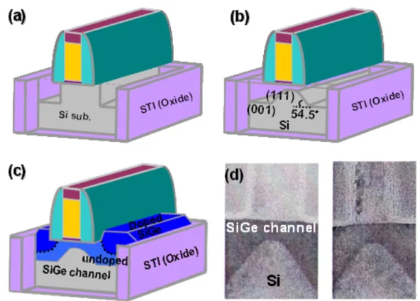
Figure 1. A novel technique of etching and deposition process sequence to create a suspending gate stack and to fill the ESC; the TEM picture shows the ESC structure.
passivation to show potentially superior hole mobility and superior gate oxide integrity. It is believed that the ESC structure is a very promising candidate in the nanodevice era with the beautiful essence of low cost and standard p-MOSFET process compatibility.
2. Device design and fabrication
A series of p-FETs with shallow trench isolation (STI) and arsenic well implantation to control Vt in the ESC devices,
which has a smaller energy gap (Eg) than the Si substrate
were fabricated on 300 mm [1 1 0]/(0 0 1) Si wafers. After this process, 1.5 nm thick SiON with 10–15% of nitrogen concentration was formed by a rapid thermal process (RTP) and decoupling plasma nitridation (DPN). 30 nm gate length and 15 nm nitride spacer critical dimension (CD) were achieved. A conventional reactive ion etching (RIE) process, named dry etch-1 (figure 1(a)), created a recessed region of 60 nm in depth. Subsequently, the samples were put into a reduced pressure chemical vapour deposition (RPCVD) chamber at 700◦C for the novel technique of dry etch, named dry etch-2, which is an in situ etch process of Cl2or HCl gas to etch away
silicon along the (1 1 1) plane with 54.5◦to create a suspending gate stack (figure 1(b)). By the well-designed depth of dry etch-1 of over 50 nm and the crystalline characteristic of dry etch-2, we can perform calculations involving trigonometric functions to obtain a suspending gate stack. An undoped SiGe epitaxial layer (Ge∼ 40 at%) to fill up the channel and a doped SiGe layer to fill up S/D were deposited at 700◦C without the necessity of a thin Si surface passivation layer in the same RPCVD chamber. The epitaxial SiGe layer was conjointly
formed in compressive mode at the channel as well as the lightly doped drain (LDD) and S/D regions (figure1(c)). The arsenic (As) pocket implantation and S/D implantation as well as a spike rapid thermal anneal (RTA) were conducted after the ESC formation. Subsequent processes were carried out to fabricate the 28 nm p-MOSFETs. The transmission electron microscopy (TEM) images of the almost dislocation-free ESC show a good crystalline ESC between the gate oxide and the underlying Si substrate, as shown in figure 1(d). The ESC devices are compared with the reference Si p-FETs with S/D strained SiGe.
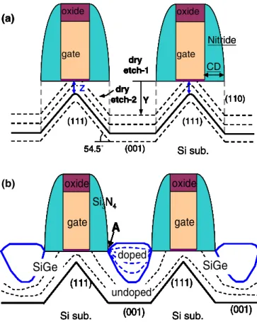
Figure2(a) shows the design of our ESC by defining the various depths of dry etch-1, Y , at 30 nm gate length and 15 nm nitride spacer CD, and then obtaining the corresponding SiGe channel depth, Z, which is calculated by the trigonometric functions of the lattice plane (1 1 1) with 54.5◦between (0 0 1) planes. Figure2(b) illustrates the profile of the ESC and S/D SiGe region. After in situ dry etch-2 to obtain a suspending gate stack, the undoped SiGe channel region was deposited first to form the SiGe channel. The SiGe channel results in a higher hole mobility than the Si channel device. The highly doped SiGe was subsequently deposited in the S/D region and it can lead to a lower S/D resistance and a better device performance. The optimized well implantation and the subsequent LDD and pocket implantation were performed to adjust the Vt in the
SiGe channel ECS device.
3. Device result
Figures3and4show the Vtroll-off and Gmimprovement on the
ESC p-FETs and conventional strained Si p-FETs (S/D SiGe 2
(111) (001) (110) gate oxide (111) gate oxide 54.5 Y Z dry etch-1 dry etch-2 (111) (001) (110) gate oxide (111) gate oxide 54.5 Y Z dry etch-1 dry etch-2 (111) (001) (111) (001)
A
undoped dopedSiGe
SiGe
gate Si3N4 oxide gate oxide (111) (001) (111) (001)A
undoped doped (111) (001) (111) (001)A
undoped dopedSiGe
SiGe
gate Si3N4 oxide gate oxide (a) (b) Si sub. Si sub. Si sub. (111) (001) (110) gate oxide (111) gate oxide 54.5 Y Z dry etch-1 dry etch-2 (111) (001) (110) gate oxide (111) gate oxide 54.5 Y Z dry etch-1 dry etch-2 (111) (001) (111) (001)A
undoped dopedSiGe
SiGe
gate Si3N4 oxide gate oxide (111) (001) (111) (001)A
undoped doped (111) (001) (111) (001)A
undoped dopedSiGe
SiGe
gate Si3N4 oxide gate oxide (111) (001) (110) gate oxide (111) gate oxide 54.5 Y Z dry etch-1 dry etch-2 (111) (001) (110) gate oxide (111) gate oxide 54.5 Y Z dry etch-1 dry etch-2 (111) (001) (111) (001)A
undoped dopedSiGe
SiGe
gate Si3N4 oxide gate oxide (111) (001) (111) (001)A
undoped doped (111) (001) (111) (001)A
undoped dopedSiGe
SiGe
gate Si3N4 oxide gate oxide (a) Si sub. Si sub. Si sub. CD Nitride (111) (001) (110) gate oxide (111) gate oxide 54.5 Y Z dry etch-1 dry etch-2 (111) (001) (110) gate oxide (111) gate oxide 54.5 Y Z dry etch-1 dry etch-2 (111) (001) (111) (001)A
undoped dopedSiGe
SiGe
gate Si3N4 oxide gate oxide (111) (001) (111) (001)A
undoped doped (111) (001) (111) (001)A
undoped dopedSiGe
SiGe
gate Si3N4 oxide gate oxide (a) Si sub. Si sub. Si sub. (111) (001) (110) gate oxide (111) gate oxide 54.5 Y Z dry etch-1 dry etch-2 (111) (001) (110) gate oxide (111) gate oxide 54.5 Y Z dry etch-1 dry etch-2 (111) (001) (111) (001)A
undoped dopedSiGe
SiGe
gate Si3N4 oxide gate oxide (111) (001) (111) (001)A
undoped doped (111) (001) (111) (001)A
undoped dopedSiGe
SiGe
gate Si3N4 oxide gate oxide (111) (001) (110) gate oxide (111) gate oxide 54.5 Y Z dry etch-1 dry etch-2 (111) (001) (110) gate oxide (111) gate oxide 54.5˚ Y Z dry etch-1 dry etch-2 (111) (001) (111) (001)A
undoped dopedSiGe
SiGe
gate Si3N4 oxide gate oxide (111) (001) (111) (001)A
undoped doped (111) (001) (111) (001)A
undoped dopedSiGe
SiGe
gate Si3N4 oxide gate oxide Si sub. Si sub. Si sub. CD NitrideFigure 2. (a) illustrates the design of the ESC by defining the various depths of dry etch-1, Y , then obtaining the corresponding SiGe channel depth, Z; (b) shows the profile of the ESC and the S/D SiGe region. 0 0.05 0.10 0.15 0.20 0.25 0.30 0.35 0.40 800 450 215 81 54 45 35 32 27 Lmask (nm) ESC device SD SiGe 0 0.05 0.10 0.15 0.20 0.25 0.30 0.35 0.40 800 450 215 81 54 45 35 32 27 Lmask (nm) ESC device SD SiGe Vt_lin Vt_sat Strained Si pFETs ESC pFETs Vt_lin Vt_sat 0 0.05 0.10 0.15 0.20 0.25 0.30 0.35 0.40 800 450 215 81 54 45 35 32 27 Lmask (nm) ESC device SD SiGe 0 0.05 0.10 0.15 0.20 0.25 0.30 0.35 0.40 800 450 215 81 54 45 35 32 27 Lmask (nm) ESC device SD SiGe Strained Si pFETs ESC pFETs 0 0.05 0.10 0.15 0.20 0.25 0.30 0.35 0.40 800 450 215 81 54 45 35 32 27 Lmask (nm) ESC device SD SiGe 0 0.05 0.10 0.15 0.20 0.25 0.30 0.35 0.40 800 450 215 81 54 45 35 32 27 Lmask (nm) ESC device SD SiGe 0 0.05 0.10 0.15 0.20 0.25 0.30 0.35 0.40 800 450 215 81 54 45 35 32 27 Lmask (nm) ESC device SD SiGe 0 0.05 0.10 0.15 0.20 0.25 0.30 0.35 0.40 800 450 215 81 54 45 35 32 27 Lmask (nm) ESC device SD SiGe 0 0.05 0.10 0.15 0.20 0.25 0.30 0.35 0.40 800 450 215 81 54 45 35 32 27 Lmask (nm) ESC device SD SiGe 0 0.05 0.10 0.15 0.20 0.25 0.30 0.35 0.40 800 450 215 81 54 45 35 32 27 Lmask (nm) ESC device SD SiGe Vt_lin Vt_sat Strained Si pFETs ESC pFETs Vt_lin Vt_sat 0 0.05 0.10 0.15 0.20 0.25 0.30 0.35 0.40 800 450 215 81 54 45 35 32 27 Lmask (nm) ESC device SD SiGe 0 0.05 0.10 0.15 0.20 0.25 0.30 0.35 0.40 800 450 215 81 54 45 35 32 27 Lmask (nm) ESC device SD SiGe Strained Si pFETs ESC pFETs
Vt_lin & Vt_sat (volt)
Figure 3. ESC device demonstrating Vthslightly better than or comparable to that of the conventional strained Si p-FETs with the S/D SiGe devices.
p-FETs), respectively. It has been reported that boron out-diffusion from LDD regions causes the worse short channel control in the conventional strained Si p-FETs. The epitaxial SiGe layer of the ESC structure in the LDD region can retard the out-diffusion of boron and has a better short channel con-trol. The optimized well implantation and As pocket implan-tation can contribute to the healthy Vtroll-off behaviour and Vt
position for the application on current advanced transistors in figure3. Due to the higher hole mobility in SiGe than in the Si channel, figure4demonstrates that the ESC p-FETs show 26%
Strained Si pFETs (S/D SiGe) Embedded SiGe channel (ESC) pFETs
Gm (ms/um) 0 9E5 3E5 1.2 E4 6E5 0 0.2 0.4 0.6 0.8 1.0 1.2 Vg (Volt) 26% 0 9E5 3E5 1.2 E4 6E5 0 0.2 0.4 0.6 0.8 1.0 1.2 26% Strained Si pFETs (S/D SiGe) Strained Si pFETs (S/D SiGe) Embedded SiGe channel (ESC) pFETs
Gm (ms/um) 0 9E5 3E5 1.2 E4 6E5 0 0.2 0.4 0.6 0.8 1.0 1.2 Vg (Volt) 26% 0 9E5 3E5 1.2 E4 6E5 0 0.2 0.4 0.6 0.8 1.0 1.2 26%
Figure 4. ESC device showing 26% p-FET Gmgain higher than that of the conventional strained Si p-FETs with the S/D SiGe devices.
-35 -28 -21-14 -7 0 7 14 21 28 35 80 90 100 110 120 130 140 150 H o le m o b ility
S
D
X=50 nm X=30 nm X=15 nm X<0 nm Simulation conditions: Lg=30nm, Si3N4CD=15nm, Recess depth=60nm SiGe=60nm, 40 at.%Ge Channel (nm) 160 X Source Drain (100) (111) -35 -28 -21-14 -7 0 7 14 21 28 35 80 90 100 110 120 130 140 150 H o le m o b ilityS
D
X=50 nm X=30 nm X=15 nm X<0 nm Simulation conditions: Lg=30nm, Si3N4CD=15nm, Recess depth=60nm SiGe=60nm, 40 at.%Ge Channel (nm) 160 X Source Drain (100) (111)Figure 5. Simulation of the hole mobility of the ESC structure and the S/D SiGe structure. The epitaxial SiGe layer sharing more area of the Si channel shows higher channel Si stress induced mobility enhancement.
Gmperformance enhancement, higher than that of the strained
Si p-FETs with S/D SiGe under a comparable threshold volt-age (Vth). Higher hole mobility and Gmimprovement can lead
to a better device performance in the strained SiGe channel of the ESC p-FETs than the strained Si p-FETs.
Figure5simulates the hole mobility in the ESC structure and the strained Si structure with the S/D SiGe. We calculate the hole mobility by the change in effective mass and carrier scattering with the stress treatment and different Ge concentrations in the SiGe channel. The stress distribution is simulated by ANSYS simulation tool first, and the SiGe effective mass, the change in scattering rate and the corresponding hole mobility with stress are calculated by the 6× 6 k.p (Kroning–Penney) model. Both SiGe material in the channel and compressive stress in the channel benefit higher hole transport mobility. On the other hand, we can also observe that when the epitaxial SiGe layer shares more Si substrate region in the hole conduction channel, which means the proximity of the intra-recess spacing, X becomes smaller, the hole mobility in the strained Si can be further enhanced. Hence, the average hole mobility in the device increases with decreasing Si region X. The hole mobility of the ESC structure is enhanced to the highest value as the epitaxial SiGe layer filled up the entire channel region. Based on the simulation,
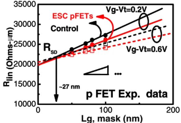
J. Phys. D: Appl. Phys. 45 (2012) 495102 M H Yu et al 0 100 200 10000 15000 20000 25000 30000 35000 Vg-Vt=0.6V
R
SDp FET Exp. data
SiGe channel Control R lin (Ohm s -m ) Gate length (nm) … ~27 nm Vg-Vt=0.2V ESC pFETs Lg, mask (nm) 0 100 200 10000 15000 20000 25000 30000 35000 Vg-Vt=0.6V
R
SDp FET Exp. data
SiGe channel Control R lin (Ohm s -m ) Gate length (nm) … ~27 nm Vg-Vt=0.2V ESC pFETs Lg, mask (nm) µ
Figure 6. Rlinas a function of gate length showing mobility enhancement for the ESC p-FET device.
Figure 7. Ion–Ioffcharacteristic of p-FET devices showing a performance improvement gain of 8% for ESC wafers. No other strain element such as a compressive stressed nitride liner was used in either the control or the ESC devices.
the ESC structure has a hole mobility of about 56% higher than that of the S/D SiGe structure. However, only 26% Gm
gain enhancement is observed for ESC p-FET devices in our experiment. It is conjectured to the existence of the channel resistance and S/D contact resistance [14]. The superior p-FET performance of the ESC structure is considered as a highly potential candidate in the future nano-p-MOSFET node and FinFETs.
Figure 6 shows a clear difference in the slope between the control (strained Si device with S/D SiGe) and the ESC p-FET device in the Rlin (resistance in the linear region of
the I –V curve) versus Lg, mask (gate length by mask) plot
[15]. This obvious difference in slopes results from a 26% enhancement in transconductance gain by the higher carrier transport mobility for the ESC p-FETs than for the control wafer under the comparable effective gate length, Lg,eff, which
was electrically extracted by the Terada method in the linear region of the current–voltage relationship [16].
In fact, the effect of this increased mobility can be seen in the Ion–Ioffcharacteristics shown in figure7. In order to isolate
the higher mobility effect of ESC alone, no other strain element such as a compressive stressed nitride liner was incorporated into either the control or the ESC p-FET devices. Vt roll-off
and overlap capacitance were well matched. At a fixed Ioff
value, the drive current gain of the ESC p-FETs with moderate Ge content is∼8% higher than that of the control devices.
Figure 8. (a) Ids–Vdsand (b) Ids–Vgscharacteristics of 28 nm Lg p-FET with the control wafer and the ESC device.
510 520 530 540 550
GeO
Intensity of O1s
Binding Energy (eV)
SiO2 Blanket SiGe with oxidation 106 101 102 103 104 105 510 520 530 540 550 GeO SiO2 SiGe on blanket oxide film 10 10 10 10 10 10 510 520 530 540 550 GeO Intensity of O1s
Binding Energy (eV)
SiO2 Blanket SiGe with oxidation 106 101 102 103 104 105 510 520 530 540 550 GeO SiO2 SiGe on blanket oxide film 10 10 10 10 10 10
Figure 9. XPS analysis data; no Ge–O bonding is observed for the grown SiGe layer on the SiO2, which means only Si–O bonding is observed in our ESC device.
As shown in figure8(a), the Id–Vgsplot shows higher ion
drive current for ESC devices than for the control of strained Si with S/D SiGe devices. On the other hand, SiGe channel devices, in general, would show a higher Ioff current than the
strained Si devices due to the small band-gap in the SiGe material. Therefore, we use the additional arsenic well implant of about 2× 1012cm−2 to suppress Ioff in our SiGe channel
devices (ESC), the same as the control strained Si devices, and then make a clear device performance comparison. Figure8(b) shows the Id–Vds characteristics of the control and the ESC
p-FET.
Figure9 shows the x-ray photoelectron spectrum (XPS) analysis data and indicates that only Si–O bonding is observed in our ESC device. The fact that no Ge–O bonding is observed for the grown SiGe layer on SiO2 reflects that the in situ
etch does not damage with gate oxide SiO2at 700◦C and the
epitaxially deposited SiGe does not react with the suspending stacked gate dielectric SiO2 to form GeOx at the deposition
temperature of 700◦C. The chemical equations for describing the formation of the ESC structure are expressed as follows:
2Cl2(g)+ Si(s)→ SiCl4(g) T = 700◦C (1)
4HCl(g)+ Si(s)→ SiCl4(g)+ 4H(g) T = 700◦C (2)
4HCl(g)+ SiO2(s)→ SiCl4(g)+ 2H2(g)+ O2(g) T >1800◦C
(3) 4
Figure 10. ESC device showing comparable gate oxide leakage performance with the strained Si p-FETs, because there is no GeOx
composition during SiGe deposition according to the XPS analysis.
12HCl(g)+ Si3N4(s)→ 3SiCl4(g)+ 4NH3(g) T >1800◦C
(4) GeH4(g)+ SiO2(s)→ SiH4(g)+ 2GeO2(s) T >1800◦C. (5)
In the literature, the conventional SiGe channel without Si surface passivation formed a gate dielectric with the interface composed of GeOx/SiGe, which caused numerous interfacial
defects and became one of the most crucial issues in the SiGe channel p-MOSFETs [17,18]. Then, Si surface passivation is necessary to avoid GeOx formation, and a thin Si passivation
layer of about 1 nm with good uniformity is very difficult for mass production. Therefore, this approach of the ESC structure can achieve the benefit of a SiGe channel without Si passivation to obtain a superior interface quality in addition to a higher channel mobility in SiGe.
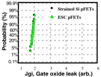
Figure10compares the gate leakage current between the ESC device and the control strained Si devices with S/D SiGe. The comparable value between these two devices demonstrates that the insulator layer and the interface between SiO2 and
the semiconductor surface are good with only Si–O bonding observed in the ECS device. Due to the process design of the ESC, it cannot demonstrate a full SiGe channel for a large gate length (Lg), such as an MOS capacitor. Therefore, we cannot
extract the interfacial defect (Dit) as an index to evaluate the integrity of the gate oxide, instead, we use the gate leakage current as an indicator for the integrity of the gate oxide of the ESC device.
4. Conclusion
A novel technique of creating an embedded SiGe channel (ESC) structure without Si surface passivation shows a p-FET
Gmgain of 26% higher than that of the conventional strained Si
p-FETs with source/drain (S/D) SiGe for 28 nm p-MOSFETs. Better Rsd and device gain of 8% in the Ion–Ioff plot and
improved swing slope in the Id–Vgscharacteristics all indicate
enhanced hole mobility in the ESC p-FETs than the control wafer. According to the XPS analysis, the gate oxide leakage and the reliability of the constant voltage stress were also
examined to recognize the superior SiGe/SiO2interface with
Si–O bonding, and no Ge–O bonding. The novel etch
process to create the ESC structure is considered as a very promising technique for 28 nm p-MOSFETs and future N/P SiGe channels in FinFETs.
Acknowledgments
The authors would like to thank the National Science Council of the Republic of China, Taiwan, for financially supporting this research under Contract No NSC 97-2218-E-009-005. Taiwan Semiconductor Manufacturing Co. Ltd, (tsmc) and National Nano-Device Laboratories (NDL) are commended for their assistance with device fabrication. Ted Knoy is appreciated for his editorial assistance.
References
[1] Thompson S et al 2002 International Electron Device Meeting (San Francisco, CA) pp 61–4
[2] Ghani T, Armstrong M, Auth C, Bost M, Charvat P, Glass G and Hoffmann T 2003 International Electron Devices Meeting (Baltimore, MD) pp 978–80
[3] Ueno T, Rhee H S, Lee S H, Lee H, Shin D S, Jin Y-S, Maeda S and Lee N-I 2005 Dramatically enhanced performance of recessed SiGe source–drain PMOS by in situ etch and regrowth technique (InSERT) VLSI (Tokyo) p 24
[4] Chidambaram P R et al 2004 35% Drive current improvement from recessed-SiGe drain extensions on 37 nm gate length PMOS VLSI Symp. Technology Digest (Hawaii) p 48 [5] Verdonckt-Vandebroek S, Crabb E F, Meyerson B S,
Harame D L, Restle P J, Stork J M C and Johnson J B 1994 SiGe-channel heterojunction p-MOSFET’s IEEE Trans. Electron Devices41 90
[6] Andrieu F et al 2003 SiGe channel p-MOSFETs scaling-down in European solid-state device research 33rd Conf. on ESSDERC ’03 (Helsinki)
[7] Zimmarman P et al 2006 High performance Ge pMOS devices using a Si-compatible process flow Technical Digest—Int. Electron Devices Meeting (San Francisco, CA) P655 [8] Oh J 2009 Additive mobility enhancement and off-state current reduction in SiGe channel pMOSFETs with optimized Si Cap and high-k metal gate stacks Int. Symp. on VLSI Technology, Systems and Application (VLSI-TSA) (Tokyo) pp 22–3
[9] Yee-Chia Yeo and Chenming Hu 2000 Enhanced performance in sub-100 nm CMOSFETs using strained epitaxial silicon–germanium IEDM (San Francisco, CA) pp 753–6 [10] Franco J 2011 On the impact of the Si passivation layer
thickness on the NBTI of nanoscaled Si0.45Ge0.55 pMOSFETs Microelectron. Eng.88 1388–91
[11] Hattangady S V, Mantini M J, Fountain G G, Rudder R A and Markunas R J 1992 The role of an ultrathin silicon interlayer at the SiO2–Ge interface J. Appl. Phys. 71 3842
[12] Taoka N, Harada M, Yamashita Y, Yamamoto T, Sugiyama N and Takagi S-i 2008 Effects of Si passivation on Ge metal–insulator–semiconductor interface properties and inversion-layer hole mobility Appl. Phys. Lett.92 113511 [13] Lee C H, Nishimura T, Tabata T, Wang S K, Nagashio K,
Kita K and Toriumi A 2010 Ge MOSFETs performance: impact of Ge interface passivation IEDM (San Francisco, CA) p 416
[14] Dieter K Schroder 2006 Semiconductor Material and Device Characterization 3rd edn (Hoboken, NJ: Wiley) p 501
J. Phys. D: Appl. Phys. 45 (2012) 495102 M H Yu et al [15] Rim K, Narasimha S and Longstreet M 2002 Low field
mobility characteristics of sub-100 nm unstrained and strained Si MOSFETs IEEE IEDM (San Francisco, CA) p 43
[16] Ortiz-Conde A, Garc´ıa S´anchez F J and Liou J J 2000 On the extraction of threshold voltage, effective channel length and series resistance of MOSFETs J. Telecommun. Inform. Technol. 3–4 43–58
[17] Matsubara H, Sasada T, Takenaka M and Takagi S 2008 Evidence of low interface trap density in GeO2/Ge metal–oxide–semiconductor structures fabricated by thermal oxidation Appl. Phys. Lett.93 032104 [18] Prabhakaran K, Maeda F, Watanabe Y and Ogino T 2000
Thermal decomposition pathway of Ge and Si oxides: observation of a distinct difference Thin Solid Films 369 289