142 IEEE ELECTRON DEVICE LETTERS, VOL. 28, NO. 2, FEBRUARY 2007
The Investigation of Post-Annealing-Induced Defects
Behavior on 90-nm In Halo nMOSFETs
With Low-Frequency Noise and
Charge-Pumping Measuring
Chieh-Ming Lai, Yean-Kuen Fang, Wen-Kuan Yeh, C. T. Lin, and T. H. Chou
Abstract—In this letter, we investigated the effects of post-annealing on indium (In) halo-induced defects for 90-nm nMOSFETs with both low-frequency noise and charge-pumping (CP) current measuring methods. The noise in In halo devices with and without a post-annealing is lower and higher than that in Boron-halo devices, respectively. Additionally, with increase of annealing time, the noise is decreased for the measuring frequency less than 1 kHz due to the efficient elimination of oxide defects. For frequency larger than 1 kHz, the longer annealing time induces a larger quantity interface defects thus enhancing the generation of noise in high frequency. The results are nicely supported by the measurements of gate integrity and CP currents. Index Terms—Charge pumping (CP), indium halo, low-frequency (LF) noise, post-annealing.
I. INTRODUCTION
I
N SUBMICROMETER regime, the short-channel effect is a severe issue for threshold voltage control and power saving. The indium (In) halo structure has been used successfully and extensively in fabricating abrupt junction profiles in sub-micrometer nMOSFET for its low-diffusion constant [1]–[3]. However, the large effective mass of In also causes serious ion bombardment to generate a large amount of defects (oxide defects and interface defects) thus increasing leakage current and degrading a device’s performance [4]. Therefore, adopting post thermal annealing (PA) after In halo implantation is indis-pensable for In halo devices to alleviate the defects caused by the In ion bombardment.In the past, In halo implantation caused performance dations and the impacts of various PA processes on the degra-dations have been studied with conventional dc analyses [5]. However, these previous studies, did not concern the effects of various PA processes on gate oxide and Si/SiO2 interface
defects, which are always the key factors of the degradations.
Manuscript received September 5, 2006. This work was supported by the National Science Council of Taiwan under Contract of NSC 95-2221- E-006-415 and NSC 94-2215-E-390-001. The review of this letter was arranged by Editor K. DeMayer.
C.-M. Lai, Y.-K. Fang, C. T. Lin, and T. H. Chou are with the Institute of Microelectronics, National Cheng Kung University, Tainan 70101, Taiwan, R.O.C. (e-mail: ykfang@eembox.ee.ncku.edu.tw).
W.-K. Yeh is with the Department of Electrical Engineering, National University of Kaohsiung, Kaohsiung 811, Taiwan, R.O.C.
Color versions of one or more of the figures in this letter are available online at http://ieeexplore.ieee.org.
Digital Object Identifier 10.1109/LED.2006.889237
Additionally, the advanced deep-submicrometer In halo devices are operated under radio frequency range; therefore, the dc analysis results are not consistent with real applications and need conventional ac measuring techniques such as the charge-pumping (CP) measurement [6]. Nevertheless, the CP method is only available for interface defects. Therefore, in this pa-per, the low-frequency (LF) noise measurement is added for its high sensitivity to both gate oxide and Si/SiO2 interface
defects [7]–[10].
This letter reports the effects of PA on device degradations and distinguishes the effects on oxide defects from the interface defects by LF noise measurement. To our knowledge, using LF noise measurement to analyze the defects affected by PA on In halo nMOSFET has not reported. Experimental results show that the effects of PA on the performances of In halo nMOSFET are similar to dc electrical analysis in the region of f < 1 kHz; but more interface defects are generated for f > 1 kHz due to the long annealing time, which is contrary to the dc measured results. Additionally, the noise in In halo devices with and with-out the post-annealing is lower and higher than that in Boron (B) halo devices, respectively. Thus, processing the PA after the In halo implantation is indispensable for In halo devices to alleviate the defects caused by the In ion bombardment; but should be compromised between the elimination of gate oxide defects and the generation of interface defects.
II. EXPERIMENTS
The samples of 90-nm In halo nMOSFET with a 1.2-µm width were prepared by a leading-edge 90-nm CMOS technol-ogy using shallow trench isolation and a retrograde well. First, a nitrided gate oxide with electrical oxide thickness∼16 Å was grown with rapid thermal oxidation in nitrided-oxide ambient and followed by poly-Si layer deposition. After gate pattern-ing, n+ source/drain extensions were formed by arsenic (As)
implantation with 100 keV and a dose of 1012∼ 1013 cm−2. To form a halo structure, In implantation was implemented with a dose of 2E13 cm−2 and 150-keV implantation energy from a 20◦ tilted angle. Additionally for comparison, B halo samples were prepared with the same condition as that of the In halo samples except the halo implantation. Because Boron atoms diffuse rapidly during PA, In general, no any PA is implemented for B halo devices. For the In halo samples,
LAI et al.: INVESTIGATION OF POSTANNEALING-INDUCED DEFECTS BEHAVIOR 143
Fig. 1. Noise power spectral density (SId/Id2) from 10 Hz to 10 kHz for
90-nm halo-implanted nMOSFETs with no post-annealing.
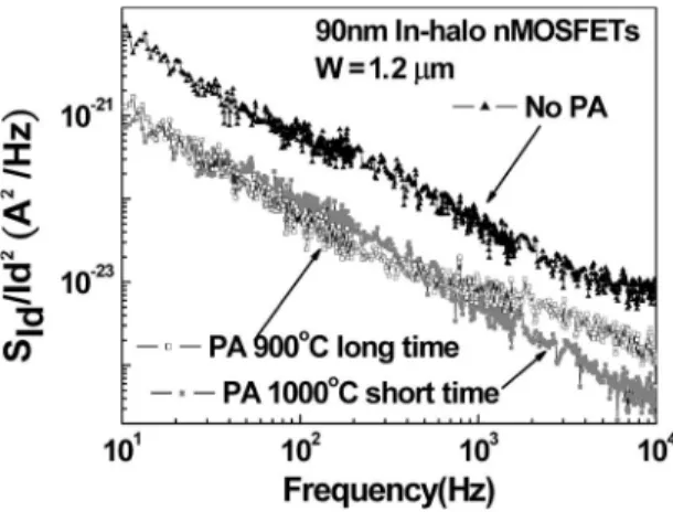
Fig. 2. Noise power spectral density (SId/Id2) from 10 Hz to 10 kHz for
90-nm In halo nMOSFETs under various post-annealing treatments.
various PA treatments were adopted using the rapid thermal process (RTP) at 900 ◦C long time (60 s) to 1000 ◦C short time (20 s). After the fabrication of a 0.1-µm-thick composite oxide/SiN spacer, an n+deep source/drain junction was formed
with As+implantation and activated by 1000◦C 20 s annealing. Finally, the wafers were annealed using an RTP, followed by the CoSi2 salicidation process, and then processed through a
standard backend flow to complete the samples. III. RESULTS ANDDISCUSSIONS
Fig. 1 shows the measured power spectral density (SId/Id2)
of 1/f noise from 10 to 10 kHz for 90-nm B and In halo nMOSFETs without PA process, respectively. Devices were measured in subthreshold region under VD = 0.1 V and VG−
VTH= 0.8 V using a BTA9812B noise analyzer in
conjunc-tion with an HP35670A dynamic signal analyzer. Obviously, without a PA, the noise in In halo device is higher than that in B halo one. Because the 1/f noises are major come from the defects in gate oxide and oxide/Si interface [7]–[10], thus the higher noise in In halo devices implies that more defects were generated to injure device’s dc performances, i.e., worse subthreshold swing, larger gate leakage current, and worse hot-carrier reliability etc. Various PA treatments were adopted after halo implantation to remove the defects. The noise of
Fig. 3. Gate oxide leakage distributions for nMOSFETs with In and B halo structures under various postannealing treatments.
Fig. 4. CP currents for 90-nm In halo nMOSFETs under various post-annealing treatments. The inset shows the Nitextracted from the ICPMAX.
In halo devices with two different PA treatments was shown in Fig. 2. The oxide trap densities extracted from the figure are 6.28E1017 cm−3 for no PA devices, 8.24E1016 cm−3 for 1000 ◦C short time devices, and 4.73E1016 cm−3 for 900◦C long time devices, respectively. Apparently, with the PA, the noise is lower especially in the device with 900◦C and long an-nealing time (60 s) in the region of f < 1 kHz. These results are consistent with previous dc work [5]. However, for f > 1 kHz, the noise in a device with 900 ◦C long time PA is higher than that with 1000◦C short time PA (20 s), which is contrary to the dc measured results [5]. Additionally, the crossover frequency depends on the time constant and the density of the interface de-fects, i.e., shorter time constant and lower defect density result in higher crossover frequency as found previously [11]–[14]. Furthermore, these studies reported that the noise in LF and high-frequency region are major come from the oxide defects and interface defects, respectively, and increasing the annealing time will efficiently remove the oxide defects but increase the interface defects [11]–[14]. Therefore, based on the Fig. 2, the lowest oxide defects and interface defects were found in devices with 900◦C long time PA and devices with 1000◦C short time PA, respectively. The results are nicely supported by measuring the gate oxide leakages and CP currents, as shown in Figs. 3 and 4, respectively. Fig. 3 gives the cumulative probability of
144 IEEE ELECTRON DEVICE LETTERS, VOL. 28, NO. 2, FEBRUARY 2007
gate oxide leakages for both the B and In halo nMOSFETs. Devices were inspected by wafer mapping measurements. As expected, without the PA treatment, the In halo devices have more serious gate oxide leakage than the B halo devices do due to a larger number of oxide defects caused by the heavy In-ion bombardment during halo implantation. However, after the PA, the gate oxide leakages of all In-implanted samples were greatly reduced and even lower than that of the B-implanted samples especially for the devices with 900◦C long time PA. On the other hand, Fig. 4 shows the differences of the CP currents (ICP) measured in 2 MHz (ICP 2 MHz) and 1 MHz
(ICP 1 MHz). Devices with 900◦C long time PA has higher ICP
thus in turn the larger quantity of interface defects, which were deducted from the difference of measured ICP gate leakages
[15]. Besides, the decrease of ICPat higher Vghis presumably
due to the larger vertical electric field, which caused the charge to tunnel gate oxide directly without being trapped in the interface traps.
IV. CONCLUSION
In summary, without post-annealing, LF noise measurement in region of f < 1 kHz showed that the In halo implantation increases the noise due to more defects generated in gate oxide and oxide/Si interface. On the other hand, the mea-surements evidenced the 900◦C long time post-annealing can efficiently mitigate gate oxides defects. However, in region of
f > 1 kHz, devices with long time post-annealing have higher
noise due to more interface defects are generated, which is contrary to the conventionally dc measured results. Further-more, the noise in In halo devices with and without a post-annealing is lower and higher than that in B halo devices, respectively. Thus, the PA after the In halo implantation is indispensable for In halo devices to alleviate the defects caused by the In ion bombardment, and compromises between the elimination of gate oxide defects, and the generation of inter-face defects.
REFERENCES
[1] R. Gwoziecki and T. Skotnicki, “Smart pockets-total suppression of roll-off and roll-up,” in VLSI Symp. Tech. Dig., 1999, pp. 91–92.
[2] Y. Taur and E. J. Nowak, “CMOS devices below 0.1 µm: How high will performance go?” in IEDM Tech. Dig., 1997, pp. 215–218.
[3] W.-K. Yeh and J.-W. Chou, “Optimum halo structure for sub-0.1 µm CMOSFETs,” IEEE Trans. Electron Devices, vol. 48, no. 10, pp. 2357– 2362, Oct. 2001.
[4] Y. Taur, “High performance 0.1 µm CMOS devices with 1.5 V power supply,” in IEDM Tech. Dig., 1993, pp. 127–130.
[5] W.-K. Yeh, Y.-K. Fang, and M.-C. Chen, “The effect of thermal treatment on device characteristic and reliability for sub-100-nm CMOSFETs,”
IEEE Trans. Device Mater. Rel., vol. 4, no. 2, pp. 256–262, Jun. 2004.
[6] U. Cilingiroglu, “Charge-pumping spectroscopy with pulsed interface probing,” IEEE Trans. Electron Devices, vol. 37, no. 1, pp. 267–272, Jan. 1990.
[7] C. T. Sah and F. H. Hielscher, “Evidence of the surface origin of the 1/f noise,” Phys. Rev. Lett., vol. 17, no. 18, pp. 956–958, Oct. 1966. [8] M. J. Kirton and M. J. Uren, “Noise in solid-state microstructure: A new
perspective on individual defects, interface stats and low-frequency (1/f) noise,” Adv. Phys., vol. 38, no. 4, pp. 367–468, Nov. 1989.
[9] D. M. Fleetwood and J. H. Scofield, “Evidence that similar point defects cause 1/f noise and radiation-induced-hole trapping in metal–oxide–semiconductor transistors,” Phys. Rev. Lett., vol. 64, no. 5, pp. 579–582, Jan. 1990.
[10] T. L. Meisenheimer, D. M. Fleetwood, M. R. Shaneyfelt, and L. C. Riewe, “1/f noise in n- and p-channel MOS devices through irradia-tion and annealing,” IEEE Trans. Nucl. Sci., vol. 38, no. 6, pp. 1297–1303, Dec. 1991.
[11] D. M. Fleetwood, W. L. Warren, J. R. Schwank, P. S. Winokur, M. R. Shaneyfelt, and L. C. Riewe, “Effects of interface traps and border traps on MOS postirradiation annealing response,” IEEE Trans. Nucl. Sci., vol. 42, no. 6, pp. 1698–1707, Dec. 1995.
[12] J. R. Schwank, D. M. Fleetwood, M. R. Shaneyfelt, and P. S. Winokur, “Latent thermally activated interface-trap generation in MOS devices,”
IEEE Electron Device Lett., vol. 13, no. 4, pp. 203–205, Apr. 1992.
[13] B. J. Mrstik and R. W. Rendell, “Si−SiO2 interface state generation
during x-ray irradiation and during post-irradiation exposure to a hydro-gen ambient,” IEEE Trans. Nucl. Sci., vol. 38, no. 6, pp. 1101–1110, Dec. 1991.
[14] M. H. Tsai and T. P. Ma, “1/f noise in hot-carrier damaged MOSFET’s: Effects of oxide charge and interface traps,” IEEE Electron Device Lett., vol. 14, no. 5, pp. 256–258, May 1993.
[15] S. S. Chung, S.-J. Chen, C.-K. Yang, S.-M. Cheng, S.-H. Lin, Y.-C. Sheng, H.-S. Lin, K.-T. Hung, D.-Y. Wu, T.-R. Yew, S.-C. Chien, F.-T. Liou, and F. Wen, “A novel and direct determination of the interface traps in sub-100 nm CMOS devices with direct tunneling regime (12∼ 16 Å) gate oxide,” in VLSI Symp. Tech. Dig., 2002, pp. 74–75.