行政院國家科學委員會專題研究計畫 成果報告
子計畫一:砷銻化鎵/砷化鎵第二型量子井雷射(I)
計畫類別: 整合型計畫 計畫編號: NSC93-2215-E-002-023- 執行期間: 93 年 08 月 01 日至 94 年 10 月 31 日 執行單位: 國立臺灣大學電子工程學研究所 計畫主持人: 林浩雄 計畫參與人員: 蔡宗霖、萬政典、林健銘、李騏亘;、鄒李昌 報告類型: 精簡報告 報告附件: 出席國際會議研究心得報告及發表論文 處理方式: 本計畫可公開查詢中 華 民 國 95 年 2 月 4 日
行政院國家科學委員會專題研究計畫成果報告 前瞻性量子元件 子計畫一:砷銻化鎵/砷化鎵第二型量子井雷射(I) 計畫編號: NSC-93-2125-E-002-023 執行期限:93/08/01~94/10/31 主持人: 林浩雄 參與人員: 蔡宗霖、萬政典、林健銘、李騏亘、鄒李昌 執行單位: 國立台灣大學電子研究所 中文摘要 本計畫以分子束磊晶法在砷化鎵基板上成 長銻砷化鎵/砷化鎵第二型量子井雷射,並 利用共振腔長度調整雷射波長。我們利用 雷射增益峰值對波長關係的模擬,藉著與 實驗資料的擬合來獲取銻砷化鎵/砷化鎵第 二型量子井能帶排列的關係以及銻砷化鎵 的能隙。我們獲致的GaAs0.64Sb0.36/GaAs量 子井主動層其GaAsSb之彎曲係數為 -1.31 eV,而價電帶差與能隙差比為1.02。這項 研究的結果用於銻砷化鎵光電元件的設 計,並可進一步研究溫度對雷射二極體特 性的影響。 關鍵詞: 分子束磊晶,含銻化合物半導體, 銻砷化鎵量子井,能帶排列,彎曲參數。 Abstract
In this study, we fabricated GaAsSb/GaAs type-II quantum well (QW) lasers and analyzed the basic band structure of the GaAsSb/GaAs QW. Because of a peculiar band-bending effect in the QW, the emission wavelength of the laser has a blue-shift as the cavity length is shortened. We utilized this effect to investigate the band line-up of the GaAsSb/GaAs QW. Through a simulation for the self-consistent solutions for the Poisson and Schrödinger equations, the optical gain of GaAsSb/GaAs QW was calculated. By comparing the simulated blue-shift on the gain peak with the experimental results, we
can obtain the band structure of GaAsSb/ GaAs QW. The best results after fitting: the valence band offset ratio (Qv) of the
unstrained GaAs0.64Sb0.36/GaAs is 1.02, and
the unstrained band-gap bowing parameter of GaAsSb is -1.31 eV. These results can be used in the design of GaAsSb optoelectronic devices and further studies on the thermal properties of GaAsSb lasers.
Keywords: molecular beam epitaxy,
Sb-based compound semiconductor, GaAsSb quantum well, band lineup, bowing parameter.
Introduction
Recently, GaAsSb/GaAs laser, as a potential candidate for GaAs based long-wavelength lasers, has attracted great attentions and is recognized as one of the key light sources for the optical communication in the near future. Currently, high- performance GaAsSb/ GaAs VCSELs have been reported [1-2]. Devices with 1270 nm in emission wavelength and 0.45 mW in CW output power at room temperature were demonstrated [2]. To design GaAsSb/GaAs QW lasers with both long-wavelength emission and good optical gain, knowledge of the band parameters is very essential. However, previous studies on the band lineup between GaAs and GaAsSb gave quite inconsistent results. In terms of the valence-band-offset ratio Qv, i. e., the ratio of
difference, values ranging from less than 1 (type-I) to 2.1 (type-II) [3-12] were reported. Most of these works presumed that the system is type-II with valence band offset larger than the band gap difference. Nonetheless, in some very recent reports, weak type-I lineup was proposed for this alloy system. For example, Johnson et. al. suggested a more complicated band structure that GaAsSb/GaAs QW with Sb composition ~0.4 is around the turning point between weak type-I and weak type-II band line-ups [12]. In another paper, Senger et. al. reported their results obtained from the diamagnetic shift of heavy-hole exciton and proposed that GaAsSb/GaAs is weak type-I conduction band line-up [8].
The scattered results in GaAsSb/GaAs band line-up can be imputable to its complicated band structure. The band gap energy of GaAsSb has a significant bowing effect. For conduction band edge and valence band edge, their relative energies should also have bowing effect as well [5, 12]. In this respect, GaAsSb/GaAs system with different Sb composition will have different valence-band-offset ratio and even different type of band-alignment. Wang et al studied the bowing behavior of the conduction band edge [12]. The bowing parameter they reported makes the lineup of the alloy composition dependent. The lineup is type-I for Sb mole fraction less than 0.4, and type-II for larger than 0.4.
The band structure of GaAsSb/GaAs also makes the alignment determination difficult. Most of the previous studies indicated that the conduction band offset, either in type-II or weak type-I, is small. It results in the small quantum shift of the electron states in GaAsSb/GaAs QW. The valence band offset, even is large, does not significantly affect the shift of the hole states because of the heavy hole mass. Therefore, the low dependency makes the band line-up determination using transition energy characterization difficult. The worse is another effect accompanying type-II QWs or weak type-I QWs. The effect
is called band-bending effect which results from the spatial separation of electrons and holes in the QWs. This effect induces a blue shift in transition energy measurement such as photoluminescence when the excitation power increases [6,13] and makes the determination of the flat-band transition energy of the GaAsSb/GaAs QW more difficult.
In laser applications, blue-shift in EL spectrum before lasing is also observed [14]. For edge-emitting lasers, because short cavity laser needs higher gain and higher injection current, it has shorter emission wavelength than the laser with longer cavity. In other word, the higher the optical gain, the longer the peak wavelength. In this study, this dependency is utilized to investigate the band alignment of GaAsSb/GaAs QW. We grew high-quality GaAsSb/GaAs QW lasers and characterized their cavity-length dependent behaviors. From their inverse external quantum efficiency versus cavity length plots, we can find the internal loss and thus obtain the mode gain of each laser. A self-consistent calculation considering the band-bending effect and band renormalization was then employed to find the optical gain spectrum for the strained GaAs/GaAsSb QW with different carrier densities. From the calculation, we can obtain the relation between the gain peak and wavelength. By comparing the experimental and theoretical results, the best fitted band parameters, i. e., the bowing parameter for unstrained GaAsSb alloy and the valence-band-offset ratio for unstrained GaAsSb/ GaAs system, can thus be obtained. Their values are 1.31 and 1.02, respectively.
Device Fabrication
We used VG V80H solid source molecular beam epitaxy (SSMBE) to grow a single GaAsSb/GaAs QW laser structures. As4 and
Sb1 sources were from a Riber VAC500
valve cracker and an EPI 175 Sb cracker, respectively. The growth temperature of GaAsSb/ GaAs QW was 500oC, and the
Fig.1 Inverse external quantum efficiency as a function of cavity length plots.
0 500 1000 1500 2000 2500 1.0 1.5 2.0 2.5 3.0 3.5 4.0 4.5 5.0 5.5 6.0 6.5 7.0 Cavity Length (µm) SQW Laser R2244 Inver s e Ex te rnal Qu antum E fficien c y
Fig.2 Inverse external quantum efficiency as a function of cavity length plots.
growth rate was ~ 1 µm/hr. The active medium of the laser is a 7-nm-thick GaAsSb QW sandwiched between two 80-nm-thick GaAs barriers. Al0.6Ga0.4As served as the
cladding layers and they were grown at 580oC. The active layer was enclosed within an undoped separate confinement hetero-structure (SCH) composed of two 100-nm-thick AlGaAs graded index (GRIN) layers. By increasing Sb content in the GaAsSb well to 0.36, the PL emission wavelength can be extended to 1300 nm. 50-µm-wide broad stripe lasers with different cavity lengths were fabricated. The fabricated GaAsSb/GaAs QW lasers showed very low threshold currents [15].
Fig. 1 shows the spectrums of lasers with various cavity lengths. The lasing wavelength makes a blue shift as the cavity length is shorten. The lasers with short cavity have larger mirror loss and need more carrier injection to sustain the oscillation. Increasing carrier density in the QW enhances the space charge field and increases the transition energy. As shown in the figure, the largest shift can be as large as 27 nm. The dependence of inverse external quantum efficiency versus cavity length is depicted in Fig. 2. As can be seen, the internal quantum efficiency is 31% and the internal loss is 4.8 cm-1 for the QW lasers. The obtained internal losses were then used to calculate the modal gain of each laser. In the calculation, the reflectivity of the as-cleaved mirror was set to be 0.32.
Simulation
To begin with the optical gain calculation, we chose the band-gap energy of the GaAsSb and the valence-band-offset ratio of the GaAsSb/GaAs QW to construct an initial flat-band structure for the active region. In the calculation, we assumed that the GaAsSb in the QW is coherently strained on (100) GaAs substrate and considered the strain-modified band edges in the GaAsSb QW. Then we selected a carrier density for the GaAsSb/ GaAs QW and found a
self-consistent solution for the Schrödinger equation and Poisson equation. Because of the heavy compressive strain in GaAsSb QW, the intermixing between valence bands is neglected. Effective mass approximation with isotropic, parabolic dispersion was employed in this study. Since the laser is operated at high injection condition, we considered the band renormalization effect by including the relative terms into the potential energy term of the Schrödinger equation: r , XC r , H r r V V V U = + + (1) where Vr is the GaAsSb/GaAs QW potential
energy, and VH,r , VXC,r are space charge
induced Hartree term and many body effect induced exchange-correlation term respectively. The suffix r indicates a position along the growth direction. To calculate the exchange-correlation term VXC,r , we used the
following formula [16], )] r 4 . 11 1 ln( r 0545 . 0 1 [ r 2 V 0 0 0 r , xc πα + + − = (2)
where parameter α is defined by α = (4/9π)1/3 , and r
0 is the dimensionless electron
effective Bohr radius, and r is defined as (3/4n π)1/3 for bulk 3D carriers and (n π)1/2
for quantum well 2D carriers. Because the thickness of the quantum well is finite, the carriers in the quantum well are not strictly 2D systems. Thus, as the well width increases, three-dimensional characteristics will gradually emerge and become dominant. In the GaAsSb/GaAs QW for analysis, electrons are confined in the 80-nm-thick GaAs layer and holes are confined in the 7-nm-thick GaAsSb layer. Therefore, we treated electrons as 3D carriers and holes as 2D carriers for their own effective confinements. In this self-consistent calculation, 16 electron sub-bands and 4 heavy hole sub-bands were considered. The calculation gave not only the space charge field profile but also the wavefunction and carrier density for each sub-band. The material gain per unit length for a given electron sub-band 2 and a given hole sub-band 1, g21, can thus be calculated using
the following formula [17],
(3) where MT is the transition matrix element, ρr
is the reduced density of state, f1 and f2 are
the occupation probabilities of subband 1 and 2. Other notations can be referred to [17]. The total gain at transition energy E21 can be
found by summing over all possible subband pairs. Scan the transition energy from the lowest subband pairs to 1.4 eV, one can find the gain spectrum.
Results and Discussions
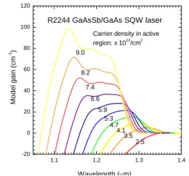
Fig. 3 shows the calculated modal gain spectrums for GaAsSb/GaAs single QW laser under carrier injection levels ranging from 2.5 to 5.3 × 10¹²/cm2. The confinement factor
of the laser is 0.0215. As can be seen, when carrier density increases, gain peak shifts toward short wavelength significantly. It is due to the band-bending effect taking place in the interface of GaAsSb/GaAs quantum well. From Fig. 3, one can easily find the
relation between the peak modal gain and peak wavelength. When a laser reaches oscillation, its modal gain is just equal to its total loss, which is the sum of the mirror loss and the internal loss. For a GaAsSb/ GaAs single QW laser with a cavity length of L, the mirror loss is (1/L)ln(1/R), while the internal loss obtained from Fig. 2 is 4.8 cm-1. Therefore, the modal gain for GaAsSb/GaAs lasers is (1.139/L + 4.8) cm-1. Through this formula, we can obtain the relation between the lasing wavelength and the cavity length. The results are shown in Fig. 3. For comparison, the experimental data is also depicted in the figure. Basically, the curvature of the curve is independent of GaAsSb band-gap energy. Changing the
) f f )( E ( ρ M E m ε nc q π g r 21 2 1 2 T 21 2 0 0 2 21= h − 1.1 1.2 1.3 1.4 -20 0 20 40 60 80 100 120 7.4 9.0 8.2 6.6 5.9 5.3 4.7 4.1 3.5 2.5 Carrier density in active region: x 1012/cm2 R2244 GaAsSb/GaAs SQW laser Mo del gai n (cm -1) Wavelength (µm)
Fig. 3 Calculated modal gain spectrums for GaAsSb/ GaAs SQW laser. The gain peak clearly shows a blue shift as the carrier density increases. 0 500 1000 1500 2000 2500 3000 1.22 1.24 1.26 1.28 1.30 1.32 1.34 1.36 wave le ng th ( µ m) cavity length (µm) Qv = 1.15 Qv = 1.02 Qv = 0.85 experiment data
Fig.4 Lasing wavelength as a function of cavity length of GaAsSb/GaAs laser. Curve represents the simulation results while the circles represent the experimental data.
band-gap energy only gives the curve a vertical shift. However, changing the valence band offset ratio of the GaAsSb/GaAs QW, Qv, not only provides the curve a vertical
shift, but also significantly affects the curvature of the curve as can be seen in Fig. 4. We repeatedly adjusted the bow parameter and valence-band-offset ratio until the difference between the experimental and theoretical results was minimized. Three curves with different Qv are depicted in Fig.
3. As can be seen, the calculated curve with Qv = 1.02 is in good agreement with the
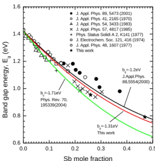
experimental data. The input parameters for this best-fitted calculation are listed as follows. The unstrained band-gap energy for GaAsSb in single QW is 0.869 eV. Note that the Sb compositions for this sample measured by XRD are 0.36. Combine with the well-known band-gap energy of GaAs and GaSb, we obtain a bowing parameter of -1.31 eV for the unstrained GaAsSb alloy. This result is in between the -1.2 eV reported by S. L. Chuang et. al. [5] and -1.71 eV reported by Wang et. al. [12] and fits most of the previous reported experimental data [18-23] quite well as shown in Fig. 5. The relative conduction and valence band edges as functions of Sb composition are shown in Fig. 6. The results from Chuang [5] and Wang [12] are also plotted. Strain effect is not considered in these three curves. Our result suggests that in the low composition range, the band alignment of GaAsSb/GaAs system is weak type-I. For higher Sb composition, it becomes type-II.
Conclusions
We have grown GaAsSb/GaAs type-II lasers and analyzed the band lineup of the QW. Due to the space charge electric field in the QW, the lasing wavelength showed a blue shift as the cavity length decreased. This phenomenon was simulated and utilized to derive the band structure of the QW. The best-fitted bowing parameter of GaAsSb alloy and valence-band-offset ratio of GaAsSb/GaAs QW are -1.31 eV and 1.02 in respectively. This finding can be used to
design GaAsSb-based devices.
References
[1] K. Nishi, T. Anan, M. Yamada, K. Kurihara, K. Tokutome, A. Kamei, and S. Sugou, 2001 Digest of the LEOS Summer Tropical Meetings 15 (2001). [2] M. Yamada, T. Anan, K. Kurihara, K.
0.0 0.1 0.2 0.3 0.4 0.5 0.6 0.8 1.0 1.2 1.4 1.6 bg=-1.71eV Phys. Rev. 70, 195339(2004) bg=-1.31eV This work Ba nd gap e nergy, E g (eV ) Sb mole fraction J. Appl. Phys. 89, 5473 (2001) J. Appl. Phys. 41, 2165 (1970) J. Appl. Phys. 54, 3433 (1983) J. Appl. Phys. 57, 4817 (1985) Phys. Status Solidi A 2, K141 (1977) J. Electrochem. Soc. 121, 416 (1974) J. Appl. Phys. 48, 1607 (1977) This work bg=-1.2eV J.Appl.Phys. 88,5554(2000)
Fig. 5 Band gap energy versus Sb mole fraction plot. Three curves with different bow parameters are depicted. Data from previous reports [18-23] are also plotted.
0.0 0.2 0.4 0.6 0.8 1.0 0.4 0.6 0.8 1.0 1.2 1.4 1.6 1.8 2.0 Ener gy (eV )
Sb mole fraction in GaAsSb
This work Chuang Wang 2.000 1.890 1.274 1.160
Fig.6 Relative energies of conduction and valence band edges as functions of Sb composition. Three curves with different bow parameters are plotted. Red curve represents the result of this study. Blue and green curves refer to [5] and [12] respectively. Note that strain effect is not included in these results.
Nishi, K. Tokutome, A. Kamer, and S. Sugou, Proceedings of 14th LEOS annual meeting 598 (2001).
[3] G. Ji, S. Agarwala, D. Huang, J. Chyi, and H. Morkoc, Phys. Rev. B 38, 10571 (1988).
[4] M. Peter, K. Winkler, M. Maier, H. Herres, J. Wagner, D. Fekete, K. H. Bachem, and D. Richards, Appl. Phys.
Lett. 67, 2639, (1995).
[5] G. Liu and S.-L. Chuang, J. Appl. Phys. 88, 5554 (2000).
[6] R. Teissier, D. Sicault, J. C. Harmand, G. Ungaro, G. Le Roux, and L. Largeau,
J. Appl. Phys. 89, 5473 (2001).
[7] X. D. Luo, C. Y. Hu, Z. Y. Xu, H. L. Luo, Y. Q. Wang, J. N. Wang, and W. K. Ge, Appl. Phys. Lett. 81, 3169 (2002). [8] R. T. Senger, K. K. Bajaj, E. D. Jones,
N. A. Modine, K. E. Waldrp, F. Jalali, J. F. Klem, G. M. Peake, X. Wei, and S. W. Tozer, Appl. Phys. Lett. 83, 2614 (2003).
[9] M. Dinu, J. E. Cunningham, F. Quochi, and J. Shah, J. Appl. Phys. 94, 1506 (2003)
[10] T. T. Chen, C. H. Chen, W. Z. Cheng, W. S. Su, M. H. Ma, Y. F. Chen, P. W. Liu, and H. H. Lin, J. Appl. Phys. 93, 9655 (2003)
[11] S. W. Ryu, and P. D. Dapkus, Semicond.
Sci. Technol. 19, 1369 (2004).
[12] J. B. Wang, S. R. Johnson, S. A. Chaparro, D. Ding, Y. Gao, Yu. G.
Sadofyev, and Y.-H. Zhang, Phys. Rev.
B. 70, 195339. (2004).
[13] D. Vignaud, X. Wallart, F. Mollot, and B. Sermage, J. Appl. Phys. 84, 2138, (1998).
[14] Weng W.Chow, Olga Blum Spahn, Hans Christian Schneider, and John F.Klem. IEEE. J. Quantum. Electron. 37, 9 (2001).
[15] P. W. Liu, M. H. Lee, H. H. Lin, and J. R. Chen, IEE Electron. Lett. 38,1354 (2002).
[16] O. Gunnarsson and B. I. Lundqvist,
Phys. Rev. B 13, 10 (1976).
[17] L. A. Coldren and S. W. Corzine, Diode
lasers and photonic integrated circuits,
John Wiley and Sons (1995).
[18] G. A. Antypas and L. W. James, J. Appl.
Phys., 41, 2165, (1970).
[19] J. L. Castano and J. Piqueras, J. Appl. Phys. 54, 3433 (1983).
[20] R. M. Cohen, M. J. Cherng, R. E. Benner, and G. B. Stringfellow, J. Appl. Phys. 57, 4817 (1985).
[21] M. B. Thomas, W. M. Coderre, and J. C. Woolley, Phys. Status Solidi A 2, K141 (1977).
[22] G. A. Antypas and R. L. Moon, J. Electrochem. Soc. 121, 416 (1974). [23] R. E. Nahory, M. A. Pollack, J. C.
DeWinter, and K. M. Williams, J. Appl. Phys. 48, 1607 (1977).