834 JOURNAL OF LIGHTWAVE TECHNOLOGY, VOL. 30, NO. 6, MARCH 15, 2012
A 25 Gbit/s Transmitter Optical Sub-Assembly
Package Employing Cost-Effective TO-CAN
Materials and Processes
Tien-Tsorng Shih, Pei-Hao Tseng, Yune-Yu Lai, and Wood-Hi Cheng, Fellow, IEEE, OSA
Abstract—A cost-effective 25 Gbit/s directly modulated trans-mitter optical sub-assembly (TOSA) employing transistor outline (TO)-CAN materials and processes is demonstrated. A high speed distributed feedback laser diode (DFB LD) chip used in the TOSA is characterized by a directly high frequency probing measurement and an equivalent circuit model according to the measurement re-sult. Using a TOSA package with TO-CAN structure and applying the deduced equivalent circuit model of the DFB LD chip in the simulation, a modified TOSA is proposed. The parasitic effect of bonding-wire and the gap induced in die bonding process is studied comprehensively to achieve an optimum configuration. Based on the simulated result, the proposed TOSA is fabricated through a conventional TO-CAN and TOSA fabrication process. The mea-sured results show that the TOSA exhibits a 3-dB bandwidth of 18.7 GHz and a clearly opening eye diagram of 25 Gbit/s. This de-veloped TOSA is potential for use in the next generation fiber net-work of 25 Gbit/s or 100 Gbit/s due to advantages of cost-effective design and mass production capability.
Index Terms—100 Gigabits Ethernet, 100 GbE-LR4, OTU4, TO-CAN, coaxial laser package, TOSA.
I. INTRODUCTION
R
ECENTLY, the standard of next generation networks of ITU-T G959.1 OTL4.4 optical transport unit 4 (OTU4), IEEE 802.3ba 100GBASE-LR4 (100 Gigabits Ethernet), and 21 Gbit/s fiber channel (20GFC) have been discussed and consented [1]–[7]. A high speed light source is one of the key components in these applications. The DFB LD nowadays is advanced and the modulation speed achieves 25 and 40 Gbit/s [8]–[13]. Conventionally, the package form factor for the above high speed laser diodes adopts a butterfly case or a particular rectangular metal box [14]–[17]. Due to the cost and manufac-turing issues, a laser module with a TO-CAN inside is widely accepted in the optical communication system [18]–[26]. Usually, the inner space of a TO-CAN package is tight and can not accommodate many electronic elements to compensate Manuscript received September 09, 2011; revised December 20, 2011; ac-cepted December 27, 2011. Date of publication December 30, 2011; date of current version February 11, 2012. This work was supported by the NSC under the Contract NSC-100-2221-E-151-032 and the MOE Program of the Aim for the Top University Plan.T.-T. Shih and Y.-Y. Lai are with the Department of Electronic Engineering, National Kaohsiung University of Applied Sciences, Kaohsiung, Taiwan (e-mail: tt@cc.kuas.edu.tw).
P.-H. Tseng and W.-H. Cheng are with the Department of Photonics, National Sun Yat-Sen University, Kaohsiung, Taiwan (e-mail: d963050002@student. nsysu.edu.tw; whcheng@mail.nsysu.edu.tw).
Color versions of one or more of the figures in this paper are available online at http://ieeexplore.ieee.org.
Digital Object Identifier 10.1109/JLT.2011.2182335
effects of the parasitical inductance and capacitance. After op-timization, some TO-CAN headers suitable for high frequency transmission have been proposed [27], [28]. The modulation speed of a directly modulated DFB laser module packaged by a TO-CAN form factor has been developed to 40 Gbit/s [29], [30]. However, the joint between the signal pin of a TO-CAN header and the inside microstrip adopts soldering process. The soldering process needs a particular technology and in-duces an extra process. In this study, a laser module without the soldering process which is compatible with an automatic TO-CAN assembly line and fits in with practical considerations for low-cost TOSA manufacturing process is proposed and demonstrated. The structure is designed theoretically through the ANSYS High Frequency Structure Simulator (HFSS) and the Agilent Advanced Design System (ADS) software. The TOSA is fabricated through an automatic TO-CAN assembly line and a laser welder. This cost-effective solution of the TOSA may be used in the next-generation fiber networks of 25 Gbit/s or 100 Gbit/s.
In Section II, a high speed DFB LD is characterized ex-perimentally and the equivalent circuit model is deduced. In Section III, the structure of a high speed TO-CAN laser module is proposed and studied theoretically. In Section IV, the fabrication and measurement results of the 25 Gbit/s TOSA is described and demonstrated. Finally, a brief conclusion is given in Section V.
II. THEFREQUENCYRESPONSE OF ADFB LDANDITS EQUIVALENTCIRCUITMODEL
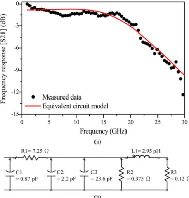
To evaluate the intrinsic frequency response of a DFB LD, the DFB LD chip was bonded on a golden microstrip of an aluminum nitride (AlN) substrate for a high frequency (HF) probing measurement. The measured frequency response of the DFB LD biased at 70 mA is shown in Fig. 1(a). The 3-dB band-width was 21.2 GHz and decreased at a higher bias current due to a thermal effect. By referring to the equivalent circuit model of a DFB LD from a previous study [25] and the mea-sured data, an equivalent circuit model of the DFB LD was es-tablished. Since HF measuring instruments and LD driving in-tegrated circuits (IC) are usually designed at an impedance of 50 , the equivalent circuit model is built accordingly and sub-jected to a terminal impedance of 50 . The diffusion capaci-tance (C3), the space charge capacicapaci-tance (C2), and the parasitic capacitance (C1) of the new equivalent circuit model were 23.6 pF, 2.2 pF, and 0.87 pF, respectively. The serial resistance (R1) was 7.25 . The inductance (L1) and the resistances (R2 and 0733-8724/$31.00 © 2012 IEEE
SHIH et al.: A 25 Gbit/s TRANSMITTER OPTICAL SUB-ASSEMBLY PACKAGE EMPLOYING COST-EFFECTIVE TO-CAN MATERIALS AND PROCESSES 835
Fig. 1. (a) The intrinsic frequency response curve and (b) the equivalent circuit model of the DFB LD.
R3) corresponding to the photon storage and the losses of pho-tons were 2.95 pH, 0.375 , and 0.12 , respectively. Above fitted parameters will change when the biased current is changed from 70 mA [25]. The simulated frequency response curve and the equivalent circuit model are shown in Fig. 1(a) and (b), respectively.
III. THEDESIGN ANDSTRUCTURE OF A25 GBIT/S TO-CAN LASERMODULE
A. The Structure of the Laser Module
The schematic diagram of the proposed TO-CAN laser module is shown in Fig. 2. The diameter of the TO-CAN header was 5.6 mm. The configuration and dimensions are similar with a conventional TO-56 header. Therefore, fabrica-tion processes and equipments are compatible. The TO-CAN header was a 5-pin structure. Two pins were used as HF signal feed-leads. The feed-leads with a diameter of 0.25 mm were used and the diameter of the feed-through holes was 0.575 mm. Another two pins were connected with the header in the backside and used to perform the grounding function. The last pin was reserved to connect with a monitor photodiode. The TO-CAN header can be used as either a single-ended or a differential package. To simplify the discussion, only the single-ended package for a directly modulated DFB LD was studied. A patterned AlN submount was placed on the surface of the stem of the TO-CAN header to accommodate the DFB LD chip and bonding wires. The DFB LD chip was bonded on the AlN submount through an AuSn soldering process. The AlN submount was glued on the surface of the stem through silver glue. An L-shaped microstrip was designed to transmit the HF signal. A ground pad surrounds the signal microstrip
Fig. 2. The schematic diagram of the proposed TO-CAN laser module.
was extended to the edge, and connects with the bottom metal. Also, the ground pad improved the transmission of the HF signal along the signal feed-lead. Two sets of bonding-wire were connected the signal feed-lead, signal microstrip, and the DFB LD chip. The HF signal was fed into the signal mi-crostrip and the DFB LD chip through the signal feed-lead and bonding-wires. Then, the HF signal was returned to the ground through the stem and grounding pins of the TO-CAN header.
B. The HF Performance Simulation of the Laser Module Under Different Wire Bonding Conditions
The bonding-wire may induce parasitic inductance and ca-pacitance and degrade the HF performance of the laser module. To investigate the variation of the HF characteristics of the laser module under different wire bonding conditions, a simulation combining the software of HFSS and the ADS was adopted [31], [32]. To improve the accuracy of the simulation, the DFB LD chip is substituted with the deduced equivalent circuit model. The diameter of the wire was 0.8 mil. Different lengths of the bonding-wire induce different parasitic inductances and will affect the high frequency performance of the module. Under a practical consideration, the length of bonding-wire (A) is set at 0.8 mm and the length of bonding-wire (B) is set at 0.4 mm. The parasitic inductance is estimated to be as the order of sub-nanohenry. Different shapes of bonding-wire induce different parasitic capacitances. For a reasonable shape, the parasitic capacitance should be as the order of femtofarad [33]. The shape of bonding-wire has a less effect compared with the length of bonding-wire in the operational frequency range. Due to a limited space on the surface of the signal feed-lead, the signal microstrip of the AlN submount, and the electrode of DFB LD chip, the maximum wire numbers of bonding-wire (A) and bonding-wire (B) were limited to five and three, respectively. The simulated 3-dB bandwidths of various wire bonding conditions are summarized in Table I. For a fixed wire number of bonding-wire (A), the 3-dB bandwidth of the laser module increased as the wire number of bonding-wire (B) increased and saturated when the wire number is larger than three. However, as the wire number of bonding-wire (B) was fixed, the 3-dB bandwidth of the laser module decreased as the wire number of bonding-wire (A) decreased. This abnormal phenomenon can be explained by a resonant peaking effect. A larger parasitic inductance induces a larger resonance and
840 JOURNAL OF LIGHTWAVE TECHNOLOGY, VOL. 30, NO. 6, MARCH 15, 2012
[25] T.-T. Shih, M.-C. Lin, and W.-H. Cheng, “High-performance low-cost 10-Gb/s coaxial DFB laser module packaging by conventional TO-CAN materials and processes,” IEEE J. Sel. Topics Quantum
Electron., vol. 12, no. 5, pp. 1009–1015, Sep./Oct. 2006.
[26] C.-C. Lin, Y.-C. Chi, H.-C. Kuo, P.-C. Peng, C. Chang-Hasnain, and G.-R. Lin, “Beyond-bandwidth electrical-pulse modulation of a TO-CAN packaged VCSEL for 10 Gbit/s injection-locked NRZ-to-RZ transmission,” J. Lightw. Technol., vol. 29, no. 6, pp. 830–841, Mar. 2011.
[27] Kyocera. [Online]. Available: http://global.kyocera.com/prdct/ semicon/semi/fo/pkg.html
[28] W. Kobayashi, K. Tsuzuki, T. Tadokoro, T. Fujisawa, N. Fujiwara, T. Yamanaka, and F. Kano, “Large bandwidth TO-CAN module with LCP based transmission line as serial 40 Gb/s 1.3/1.55- m light source,” in
Proc. Int. Semiconductor Laser Conf. (ISLC), Sep. 2010, pp. 195–196,
ThB4.
[29] W. Kobayashi, T. Tadokoro, T. Fujisawa, N. Fujiwara, T. Yamanaka, and F. Kano, “40-Gbps direct modulation of 1.3- m InGaAlAs DFB laser in compact TO-CAN package,” in Proc. OFC, Mar. 2011, pp. 1–3, OWD2.
[30] J. R. Kropp, J. A. Lott, N. N. Ledentsov, P. Otruba, K. Drogemiiller, G. Fiol, D. Bimberg, I. Ndip, R. Erxleben, U. Maass, M. Klein, G. Lang, H. Oppermann, H. Schroder, and H. Reichl, “A small form-factor and low-cost opto-electronic package for short-reach 40 Gbit/s serial speed optical data links,” in Proc. 3rd Electronic System-Integration
Technology Conf. (ESTC), Sep. 2010, pp. 1–4.
[31] T.-T. Shih, P.-H. Tseng, H.-W. Chen, C.-C. Tien, S.-M. Wu, and W.-H. Cheng, “A low-cost TO-CAN header for coaxial laser modules in 25 Gbit/s transmission applications,” IEEE Trans. Compon., Packag.
Manufact. Technol., vol. 1, no. 4, pp. 557–565, Apr. 2011.
[32] T.-T. Shih, P.-H. Tseng, Y.-Y. Lai, and W.-H. Cheng, “Compact TO-CAN header with bandwidth excess 40 GHz,” J. Lightw. Technol., vol. 29, no. 17, pp. 2538–2544, Sep. 2011.
[33] K. Mouthaan, R. Tinti, M. de Kok, H. C. de Graaff, J. L. Tauritz, and J. Slotboom, “Microwave modelling and measurement of the self- and mutual inductance of coupled bondwires,” in Proc. Bipolar/BiCMOS
Circuits and Technology Meeting (BCTM), 1997, pp. 166–169.
Tien-Tsorng Shih was born in Taiwan in 1965. He received the B.S. and Ph.D.
degrees from National Chiao Tung University, Taiwan, in 1986 and 1991, respectively.
In 1991, he joined Telecommunication Laboratories, Taiwan, as a research associate. From 1996 to 2000, he was a project manager at Chunghwa Telecom-munication Laboratories, Taiwan. In 2000, he founded Infomax Optical Tech-nology Corporation and was the CEO during 2000 to 2003. He is now a Pro-fessor at the Department of Electronic Engineering, National Kaohsiung Uni-versity of Applied Sciences, Taiwan. His main research interests include the theoretical study of optical waveguides and III-V optoelectronic devices, fab-rication of laser diodes, photodiodes, and planar lightwave circuits, packaging technology for optoelectronic devices, transceiver modules, and transmission technologies for the fiber optics communication applications.
Pei-Hao Tseng received the B.S. degree in electrical engineering from Chung
Hua University, Hsinchu, Taiwan, in 2004, and the M.S. degree in photonics and communications engineering from National Kaohsiung University of Ap-plied Sciences, Kaohsiung, Taiwan, in 2007. He is currently working toward the Ph.D. degree in the Department of Photonics, National Sun Yat-sen University, Kaohsiung, Taiwan.
His main research interests include high-speed optoelectronic packaging, transceiver modules, and microwave passive circuit for fiber optics transmis-sion and telecommunication applications.
Yune-Yu Lai received the B.S. and M.S. degree in electronic engineering from
National Kaohsiung University of Applied Sciences, Kaohsiung, Taiwan, in 2009 and 2011, respectively.
His main research interests include radio-frequency circuit design and mea-surement for telecommunication applications.
Wood-Hi Cheng (M’95–SM’00–F’10) was born in Changhua, Taiwan, on June
3, 1944. He received the Ph.D. degree in physics from Oklahoma State Univer-sity, Stillwater, in 1978.
From 1978 to 1980, he was a Research Associate at Telecommunication Lab-oratories, Taiwan. From 1980 to 1984, he was a Research Engineer at Gen-eral Optronics, Edison, NJ. From 1984 to 1991, he was a Principal Design Engineer at Rockwell International, Newbury Park, CA. From 1991 to 1994, he was an Optoelectronic Packaging Manager at Tacan Corporation. Carlsbad, CA. He is now a Professor at the Department of Photonics and Director of Southern Taiwan Opto-Electronic Center of Excellence, National Sun Yat-Sen University, Kaohsiung, Taiwan. His research and development activities have been focused on the design and fabrication of high-speed semiconductor lasers for lightwave communications, highly efficient light coupling from lasers into fibers, fiber couplers, characterization of III-V semiconductors materials, and optoelectronic packaging. His current research interests are the design, fabrica-tion, and finite-element-method analysis for laser module packaging, high-speed laser module packaging for digital lightwave systems, fabrication of high den-sity WDM components, and novel materials for electromagnetic shielding. He served as a consultant for Chunghwa Telecom Laboratories, Opto-Electronics and System Laboratories, and Chung-Shan Institute of Science and Technology, all from Taiwan.
Dr. Cheng is a Fellow of IEEE and OSA. He served as a Chair for the IEEE Lasers and Electro-Optics Society (LEOS), Taipei Chapter during 1999–2000, and served as a Chair for the OSA, Taipei Chapter during 2005–2006. He was recipient of the IEEE Photonics Engineering Achievement Award in 2010 for his contributions to design, development, and commercialization compact solid-state laser modules. He was also a recipient of the IEEE Photonics Distinguished Lecture Award in 2011.