1928 I E E E TRANSACTIONS ON ELECTRON DEVICES. VOL. 39. NO. 8. AUGUST 1992
A New Two-Dimensional Model
for
the Potential
Distribution of Short Gate-Length MESFET’s
and its Applications
Shan-Ping Chin, Student Member, IEEE, and Ching-Yuan Wu, Member, IEEE
Abstract-A new analytical technique for calculating the two- dimensional (2D) potential distribution of a MESFET device operated in the subthreshold region is proposed, in which the 2D Poisson’s equation is solved by the Green’s function tech- nique. The potential and electric-field distributions of a non- self-aligned MESFET device are calculated exactly from dif- ferent types of Green’s function in different boundary regions, and the sidewall potential at the interface between these regions can be determined by the continuation of the electric field at the sidewall boundary. The remarkable feature of the proposed method is that the implanted doping profile in the active chan- nel can be treated. Furthermore, a simplified technique is de- veloped to derive a set of quasi-analytical models for the side- wall potential at both sides of the gate edge, the threshold voltage of short gate-length devices, and the drain-induced bar- rier lowering. Moreover, the developed quasi-analytical models are compared with the results of 2D numerical analysis and good agreements are obtained.
B m Fourier coefficient for the one-dimensional (1D) potential distribution produced by the ionized impurity concentration.
Fourier coefficient for the doping profile in the ungate region at the source side N;,.(x)
c = l f o r n = O a n d c = 2 f o r n ? 1
.
Fourier coefficient for the doping profile in
)
N&(x)the ungate region at the drain side
NOMENCLATURE c = l f o r n = O a n d c = 2 f o r n 2 1
\k(x,
y)
Two-dimensional ( 2 D ) potential distribu- tion.E Dielectric permittivity of semiconductor.
4 Elemental charge (= 1.6 X C).
b Thickness of active layer.
vbi
tion.
I/Rs Gate-source voltage.
vds Drain-source voltage.
vth Threshold voltage.
k,(km) Wd(W,)
A$(Ak)
Built-in potential of a Schottky-barrier junc-
Eigenvalue of the Green’s function in the ungate (gate) region.
Position of depletion layer edge at the drain (source) side of the gate.
Fourier coefficient for the excess sidewall potential at the drain (source) side of the gate.
Nd, Fourier coefficient for the doping profile un-
der the gate
p ( x ‘ , y ’ ) Charge density.
VI Average 1D potential due to depletion charge
under the gate m
m = ~(2m - 1 ) ~
(=
c
-
v s Average sidewall potential at the source end of the gate
m
m = ~ (2m - l ) ~
-
vd Average sidewall potential at the drain end of the gate
m Manuscript received June 14, 1991; revised January 3 , 1992. This work
was supported continually for three years by the National Science Council, Taiwan, Republic of China, under Contracts NSC-78-0404-E009-26, NSC-79-0416-E009-01, and NSC-80-0416-E009-05. The review of this paper was arranged by Associate Editor M . D. Feuer.
The authors are with the Advanced Semiconductor Device Research Lab- oratory and the Institute of Electronics, National Chiao-Tung University, Hsinchu, Taiwan, Republic of China.
( V I +
m = l (2m - l ) ~
Gate length.
Element of the transfer matrix Lg
T m n
IEEE Log Number 9201207.
CHIN AND W U : POTENTIAL DISTRIBUTION OF SHORT GATE-LENGTH MESFET‘S
__
1929
Xmin Location of the minimum channel potential.
\kmin Minimum channel potential.
4 b
Channel barrier height ( = \Emin - Vgs,+ VbJ.
4;
Channel barrier height for defining the4(x) Bottom potential with respect to the source
e
h
Threshold voltage of a long-gate MESFETthreshold voltage.
potential (= \k(x, b ) - Vgs
+
V h J .(= Vbj - * l d ( b )
+
4 ; ) .
I. INTRODUCTIONHE GaAs MESFET’s are widely used in high-speed
T
logic circuit and microwave amplifier. The perfor- mance of a GaAs MESFET can be significantly enhanced by scaling down the device geometry. With the improve- ment on the process technology, a short gate-length MESFET device with sub-quarter-micrometer size can be fabricated. However, the gate-controlling capability will be reduced by the penetration of the electric field from the sidewall at both sides of the gate, and the threshold volt- age of a short gate-length device will be influenced by the drain bias.The short gate-length effect can be exactly analyzed by numerical simulation, based on a full set of semiconduc- tor device equations with reasonable boundary conditions
[ 11-[3]. However, the numerical simulation is limited by the computation time and is difficult to use in circuit anal- ysis. Furthermore, the results of numerical simulation can only provide discrete data points and are difficult to use in device optimization. The analytical model, which is generally limited by the mathematical treatment for dif- ferent device structures, becomes very difficult to develop when the multidimensional effect is obvious. However, a simple and accurate analytical model is very important for circuit analysis.
In modeling the short-channel effect in a short gate- length MESFET, the two-dimensiona (2D) Poisson’s equation satisfying different surface boundary conditions must be solved to get the 2D potential distribution. In pre- vious work in
[4],
[ 5 ] , the 2D Poisson’s equation has been solved by a Laplace reduction technique with the 2D Pois- son’s equation being divided into a 2D Laplace equation and a one-dimensional (1D) ordinary differential equa- tion, and the doping profile in the active channel has been assumed to be uniform. Moreover, in order to avoid the problems resulting from different surface boundary con- ditions the n + region was assumed to contact directly to the gate metal, and the absorption of the electric field by the depletion charges near the source/drain side was not taken into account. For a practical MESFET structure, the spacing between the n + region and the gate metal can- not be overlooked because it can reduce the short-channel effects [6] and further enhance the breakdown voltage. In a recent paper [7], the trial function method has been used to solve the 2D Poisson’s equation in the ungated part of the channel. However, this method does not clearly takethe surface boundary conditions in the ungate region into account.
Ion implantation has become a widely used process for doping the active channel and source/drain regions of a short gate-length MESFET [8]. Recently, the implanted channel profile has been considered in modeling the I-I/ characteristics of an implanted MESFET device by using 1D analysis [9]. In general, the effects of both short gate length and implanted channel profile have not been well described in the literature. In order to treat the implanted doping profile in the active channel of a MESFET device, the Green’s function technique used in MOSFET model- ing [lo] is used to solve the 2D Poisson’s equation. In this paper, a new analytical technique is developed, in which different types of Green’s function are used to cal- culate the 2D Poisson’s equation to satisfy different sur- face boundary conditions. The problem resulting from dif- ferent surface boundary conditions can be solved by matching the potential and electric field distributions. In Section 11, the boundary conditions for a non-self-aligned MESFET structure and 2D potential distribution calcu- lated by the Green’s function technique are presented. In Section 111, some approximations are made for a non-self- aligned MESFET in order to simplify the analytical equa- tions derived in Section 11. In Section IV, the developed quasi-analytical models are compared with the results cal- culated by 2D numerical simulation for a wide range of device parameters. Furthermore, the relationship between the short-channel effect and the device structure is dis- cussed. Finally, a conclusion is given in Section V .
11. THEORETICAL MODEL
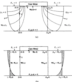
A simplified diagram showing the electric field distri- bution near the end of the gate metal for a non-self-aligned MESFET device operated in the subthreshold region is illustrated in Fig. l(a). It is shown that some of the lateral field will be terminated by the edge side of the gate metal if the device has a long gate length, and the channel po- tential is slightly affected by the lateral field. However, this is not true for a short gate-length device or when the lateral field is large. For a short gate-length MESFET, the channel potential cannot be entirely controlled by the gate bias and will be shifted by the penetration of the lateral field. From this veiwpoint, there are two factors which may play important roles for the short-channel effect in a short gate-length MESFET: one is the lateral field distri- bution at the sidewall of the gate edge; the other is the efficiency of the gate metal in terminating the lateral field. It is clear that a solution technique for the 2D Poisson’s equation satisfying suitable boundary conditions is re- quired to model the short-channel effect. However, it be- comes very difficult for a MESFET structure due to the complexity of the boundary conditions. In the following subsections, the Green’s function solution technique is proposed to solve the 2D Poisson’s equation for a non- self-aligned MESFET structure. Some assumptions and approximations are made to reduce the complexity in or- der to get a solution analytically.
1930 IEEE TRANSACTIONS ON ELECTRON DEVICES, VOL. 39, NO. 8, AUGUST 1992
(b)
Fig. 1. The schematic diagrams for a non-self-aligned MESFET structure operated in the subthreshold region. (a) Penetration of the sidewall field into the gate-controlled region and the boundary conditions used. (b) Ap- proximation used to develop an analytical model for 2D potential distri- bution.
A . Boundary Conditions
The cross-sectional view of a GaAs MESFET operated in the subthreshold region is shown in Fig. l(a), where the x coordinate represents the direction along the surface and the y coordinate represents the direction perpendicu- lar to the surface. Because the mobile carriers are negli- gibly small when the device is operated in the subthresh- old mode, the current continuity equation can be ignored. The charge distribution in the active channel is assumed to be the ionized impurity profile and the 2D Poisson’s equation can be written as
It is assumed that the effect of the surface states on the ungated semiconductor surface is very small and the elec- tric flux vanishes in these regions, hence the surface boundary conditions can be expressed as
for x
< 0 or
x> L,
(2)and
+(x, y ) l y = o = 0, for 0 I x I Lg (3)
where the gate metal is used as the reference point. For a practical GaAs MESFET, the effect of the semi- insulating substrate is very sophisticated. In order to sim-
plify the mathematical treatment without losing its valid- ity, the boundary condition in the bottom side of the ac- tive layer is set to the Neumann boundary condition and the substrate effect is neglected. The boundary condition in the bottom side of the active channel can be expressed as
E , ( x , b) = -2 y,
/Irb
= 0.(4)
When the MESFET device is operated in the subthresh- old region, the drain current is very small and the ohmic drop across the ungate regions can be neglected. The po- tentials at both sides of the depletion-layer edge can be expressed as wx3 Y)ls = Vbr - v g s \k(x, Y ) l d = vbr - vgs
+
Vds ( 5 ) and (6)where the depletion-layer edges at the source and drain sides are denoted by s and d , respectively.
Moreover, the electric field must vanish in the deple- tion-layer edges at both sides of the gate, otherwise, this field may cause a large current flow. Therefore, we may write
EEls = 0 (7)
and
where
n’
is the outward unit vector at the depletion-layer edge.B. Green s Function Solution Technique
The solution of the 2D Poisson’s equation in a finite region can be obtained by means of the Green’s function technique. Using Green’s theorem, the potential distri- bution can be expressed as [ 113
\k(x, y ) =
j j
G(x, y ; x’, y ’ )d x ’
dy’ VThe Green’s function for a rectangular domain can be expressed in a hyperbolic-sine (hyperbolic-cosine) form. However, this form cannot be directly applied to a MESFET structure shown in Fig. l(a) because the surface boundary conditions are different for the gated and un- gated regions. In order to solve the 2D Poisson’s equation with these different surface boundary conditions, the
CHIN AND WU: POTENTIAL DISTRIBUTION OF SHORT GATE-LENGTH MESFET’S 1931
Green’s function is chosen as G(x, x’; y, y’) =
W
cos (k,y) COS (k,y’)F~(x; x’; k,),
f o r x I 0 (loa>
b n = O
2 ”
G(x, x’; y, y’) = -
c
sin (k,y) sin (kmy’)FI,(x; x‘; km), (lob) b m = lfor 0 I x I L,,
where k, = n n / b , k, = (m - 1 /2) n / b ; n and m are the integers; c = 1 for n = 0 and c = 2 for n z 1; F,, F,,,
and FIrI are expressed by
f o r x ’ > x sinh (k,x’) sinh km(L, - x) &(x; x’;
k,)
= k, sinh (k,L,)i
f o r x ’ x Sinh k,(X - L,) sinh k,(L,+
Wd - x ’ ) k, sin (k,Wd) f o r x ’ > x Sinh k,(X‘-
L,) sinh k,(L,+
w d - X) k, Sinh (k,Wd) 3 f o r x ‘ < x.It is assumed that the depletion-layer edge at the source (drain) side is perpendicular to the surface at a position
- W,(L,
+
W,), as shown in Fig. l(b). It is noted that, in (1 la) and (1 IC), the hyperbolic-sine function decays exponentially for n I 1 and the influence of the sidewall potential at the source (drain) side of the gate due to the high-order terms of the Fourier component for the chargedistribution at the depletion edge can be estimated from exp (-nnW,/b) or exp (-naW,/b) for n 1 1. Since the depletion-layer edges at both sides of the gate are far away from the channel region under the gate for a non-self- aligned structure, it is expected that the channel potential is less affected by the detailed shape of the charge distri- bution in the depletion boundary at both sides of the gate because this charge distribution is described by the high- order terms of the Fourier series. The sidewall potential at both sides of the gate edge (x = 0 and
x
= L,) can be determined by using the continuation of the lateral electric field. The Fourier transformation for the sidewall poten- tial at the source/drain side of the gate edge is performed, and the Fourier coefficients of the sidewall potential can be expressed as the superposition of two partsW
\k(O, y) = ( A ;
+
B,) sin (kmy) (12a)m = l
and
W
\k(L,, y) =
c
(Ad,+
B,) sin (k,y) (12b)where B , is the Fourier coefficient of the 1D potential distribution due to the ionized impurity profile under the gate and is expressed by
m = l
b
B =
2
j’
* i d ( Y ) sin (kmy) dY (13)b o in which \Eld( y) is expressed as
Note that \ E l d ( y) in (14) is independent of bias condi-
tions; A i and Ad, are the unknown variables, which can
be determined by the boundary conditions.
Substituting
( 3 ,
( l l a ) , and (12a) into (9), the x-component electric field in the ungated region at the source side can be expressed aswhere E:,,(x, y) is the electric field due to the sidewall potential at the source side and is expressed by
W - vs W, , = I sinh (k,W,) k, cosh k,(Ws
+
x) E:,,(x, y) = -- -c
E:,,(x, y) is the electric field due to the potential at the depletion-layer edge at the source side and is expressed by
~
1932 IEEE TRANSACTIONS ON ELECTRON DEVICES, VOL. 39, NO. 8 . AUGUST 1992 E:,,@, y ) is the electric field due to the depletion charge
in the ungated region at the source side and is given by
-
sinh k,(W,+
x )dx
1
.
(18) The boundary condition in (7) is used to determine the unknown parameter W,. Integrating (15) over the active channel at x = - W,, we can obtain the following equa- tion:The average lateral electric field at the depletion-layer edge at the source side can be eliminated by using (19).
Note that the high-order terms in (1 8) do not exactly van- ish due to the assumption of the perpendicular relation between the depletion-layer edge and the surface. How- ever, the sidewall potential at the source side is not strongly affected by this approximation because these terms decay exponentially.
Similarly, the lateral electric field under the gate can be expressed as cosh km(Lg - X) sin (kmy) sinh (kmLg) m cosh (kmx) E ! , L , ( ~ , Y ) =
C
-
k m ( A i+
B,) sin (kmy) . (kmLg) m = l [cosh ( k , ~ )-
cosh km(L, - x)]. (23)Note that the doping profile N d ( x , y) under the gate is assumed to be only dependent on the y direction, thus Nd is independent of x under the gate. The lateral electric field must be continuous at x = 0, so we obtain
Substituting (15) and (20) into (24) and performing the Fourier transformation, i.e.,
5
s:
we obtain kmBm - (AS, cosh (kmL,) - A i ) k m+
sinh (kmL,) m - Vbj+
Vgs+
v,
1
+
c
Tm,k, coth (k, W,) n = l m m m-
Wss
slvb.<x>
sinh k,(W,+
x )dx
= 0 , f o r m = 1, 2, 3,-
.
9- (26)where the first term in (26) can be eliminated because
A similar treatment can be performed for the drain side to obtain another system of equations, and the results are expressed as Bmki = q N d , n / € . - v b i
+
vds - v g s Vd -+ -
wd wd and ( A i cosh (kmL,) - AS,) km sinh (kmL,)-
sinh k,(L,+
wd-
x )dx
= 0, f o r m = 1, 2, 3, *-
, 00. (28)In order to accurately model the 2D effects, one must obtain self-consistent solution from (19) and (26)-(28).
CHIN AND WU: POTENTIAL DISTRIBUTION OF SHORT GATE-LENGTH MESFET’S
However, since these equations are too complicated from the viewpoint of an analytical model, some approxima- tions will be made in the following section in order to get a simple expression.
111. A SIMPLIFIED TECHNIQUE FOR A
NON-SELF-ALIGNED MESFET
With the help of a numerical simulation, some approx- imations can be made for a non-self-aligned structure. First, it is shown that the Fourier coefficients ( A h and A i ) of the excess sidewall potential decrease rapidly with respect to the integer
m
and the first term is almost five times larger than the second term. Secondly, the hyper- bolic-sine function decreases exponentially with respect to the integer m. Therefore, it is expected that the first term is sufficient to predict the channel potential under the gate, especially for the region near the middle of the gate. As a result, the potential distribution under the gate can be approximated by the following equation:where k l (= a/2b) is the eigenvalue for the first term of the Fourier series in the channel region under the gate.
It is clearly seen that the potential distribution under the gate in (29) is expressed in terms of only two variables
( A ; and A ! ) which can be solved from (19) and (26)-(28).
Similarly, since the doping profile at both sides of the gate is assumed to be independent of x, (26) with m = 1 can be rewritten as
( A ; cosh (kIL,) - AY) kl sinh (k,L,)
1
+
- - 4 1(-@!b
wf
-v,;
+
I/,,+
v,
aw,
2E m m m qNi,n 1 - cosh (kn W,)+
C
TI,, - n = l E kn sinh (k, W,) m m+
c
Tlnkn coth (knW,)c
B m , T m l , n = 0 n = l m l = Iwhere W, can be obtained from (19) and is expressed by
(31) 2E
Note that the most complicate term in (30) is the third term, which is a coupling term between these Fourier coef-
ficients and can be rewritten as
OD m
1933
However, the solution of (30) is insensitive to this term and the ratio ( A h / A i ) is almost constant for wide ranges of device parameter and bias conditions. Therefore, this term can be simplified by the numerical analysis and is expressed as
1.4
C
Tl,,k,, coth (knW,)C
ALIT,,,,z
-/I;. (33)n = l m l = I K b
Moreover, the average potential can be approximated by
(34)
m m
- 2
V, VI
+
- A ; .a
Using (31), (33), and (34), (30) can be rewritten in a simple form
+
T(WJ (35)where a,
0,
VI, and Vp are the structure parameters, whichare independent of bias conditions and are expressed as
a 1.4 2 K =
-
coth (kIL,)+
-
a 1 2 sinh (k,L,)p = -
m B mv,
=c
m = ~ (2m-
1)a (37)Equation (35) is very similar to the result of the 1D case
with uniformly doped substrate. The second term on the left-hand side of (35) is related to the electric field pro- duced by the boundary condition at the drain side, VI is the average potential for the 1D potential distribution due to the depletion charges, Vp is the effective pinch-off po- tential and is equal to the pinch-off voltage when the ac-
1934 IEEE TRANSACTIONS ON ELECTRON DEVICES, VOL. 39. NO. 8, AUGUST 1992
tive channel is uniformly doped. The relation between the the nonuniformly doped profile and the 2D effect is clearly described in (40), in which is contributed by two terms: the first term is the 1D sidewall potential due to the ion- ized impurities under the gate, and the second term is the nonuniformly distributed depletion charges at the source side of the gate. However, from another viewpoint, v(W,) can be treated as the unmatching part of the lateral field between different regions and must be offset by the side- wall potential. If we assume that W, is sufficiently larger than b , then coth ( k , W,) G 1, and
v(
W,) can be approxi- mated byIt should be noted that 17 is independent of W , from this approximation. This means that the variable W, is elimi- nated in (35) and the unknown variables are only As and
A?. In general, this approximation is valid for different Gaussian profiles, however, the iteration must be per- formed to get a self-consistent solution for heavy doping in the ungated region.
The same treatment can be performed for the drain side. Similarly, we can obtain
where the parameters used are same as those in (35) if the structure parameters are symmetrical for both the source and the drain, i.e.,
1V. APPLICATIONS AND VERIFICATIONS
It is known that 2D effects in a short gate-length MESFET can be easily demonstrated by measuring the threshold voltage and the subthreshold current of the fab- ricated short gate-length MESFET’s. These two electrical parameter/characteristics are strongly dependent of gate length and applied drain bias. Therefore, the derived equations in Section I11 will be used to develop the thresh- old-voltage model and the drain-induced barrier lowering of a short gate-length MESFET in the following subsec- tions. Moreover, a new 2D device simulator [12] based on conventional semiconductor device equations is used to verify the accuracy of the developed analytical models.
A . Excess Sidewall Potentials and Potential Distribution
In order to calculate the potential distribution under the gate, the sidewall potential and the width of the depletion layer at both sides of the gate must be calculated first. The
first term of the Fourier coefficient for the excess sidewall potential at the source end of the gate can be solved from (31) and ( 3 9 , and the results are
and
where a l = [&If
+
q(W,)]/(aV,) - 64/(7r3a2), bl =8/(7ra), and c , = 2al/7r - 64/(7r4a2).
Similarly, the results for the drain side are
(45)
and
(46)
where a2 = [PAS
+
7 ( W d ) ] / ( a V p ) - 64/(7r3a2), b2 = 8/(7ra), and c2 = 2a2/7r - 64/(7r4a2).Note that the above equations seem to be similar to the 1D results; however, the 2D effects are properly consid- ered. It should be noted that the magnitude of A ” , A f ) is proportional to the lateral electric field at the gate edge and is strongly affected by the total amount of the deple- tion charges that can terminate the electric field. It is ex- pected that the self-aligned structure will have a larger sidewall potential than the non-self-aligned structure if the depletion edges at both sides of the gate touch the n+ re- gion.
Comparisons between the first term of the Fourier coef- ficient in the excess sidewall potential at the source side in (43) and the 2D numerical analysis are shown in Fig. 2 , in which the active channel thickness is 0.2 pm, Rp is the projected range with the reference point at the semi- conductor surface, AR, is the standard deviation or the projected straggle, and the doses of ion implantation are chosen to keep the pinch-off voltage of a long gate-length device at 1.5 V. Fig. 3(a) shows the bottom potential ver-
sus the normalized distance along the channel ( x / L g ) for various gate lengths. It is clearly seen that the central por- tion of the bottom potential distribution increases with de- creasing gate length, and good agreements between the analytical model and the 2 D numerical analysis are ob- tained for this portion which is important for accurately modeling the threshold voltage as described in the next subsection. Note that there are some discrepancies be- tween comparisons at the gate edges, especially for the case of a shorter gate-length device. These discrepancies are mainly due to the fact that A ; in (43) and A;‘ in (45)
1935 CHIN AND W U : P O T E N T I A L DISTRIBUTION OF S H O R T G A T E - L E N G T H MESFET’S
3.0- 2.5- 2.0- c C a8 .- 1.5- c 01 0 U 1.0 - 0.5- 0.0 VI- U MESFET Device: L = 0 . 5 p . b = O . l p
Gaussian’s ProGle .AR =0.06,” Vds=OV, Vbi=0.85V + + Numerical Analysis
-
Analytical Model Dose(R )= 4 5 . 1 0 ~ ~ / c m ~ ( o o v )*
I I 0.0 1.0 2.0 3.0 4.0 5.0 6.0 7.0 8.0 I L a8 3 0 U .- 3.5, 1Fig. 2. Comparisons between the first term of the Fourier coefficients in the excess sidewall potential and the 2D numerical analysis for different
Gaussian profiles in the active channel.
n
c + : N8mit.l Andyds
QO 0 1 0 2 0 3 0 4 0 5 0 6 0 7 0 8 0 9 10 Normoliml Distance, X / L ,
(a)
‘1 MESFET Device L-=O 5m, b=O 2 p
1
Gauuim’s ProGle : Dae=1.2x10¹²/cmZ, R = O . l p , A R p = O . M p
c + + ’ Numerical Analysii a 2 v C 1 v 0.5 L 0,
2
0.0E
-0.5 ov 0 m -1.0 -1.5 0.0 0.1 0.2 0.3 0.4 0.5 0.6 0.7 0.8 0.9 1.0 1.1 1.2 Normalized Distance, X / L , (b)Fig. 3. Comparisons of the bottom potential versus the normalized dis- tance ( x / L , ) between the analytical model and the 2D numerical analysis for a Gaussian profile. (a) Various gate lengths with V,, = 0 V and V,, =
-2.15 V. (b) Various V,, and Vxa = -2.15 V for gate length of 0.5 pm.
tion of the bottom potential with the drain bias is shown in Fig. 3(b). It is noted that the potential barrier is low- ered by the drain bias, and satisfactory agreements be- tween the analytical model and the 2D numerical simu- lation are obtained.
B. Threshold Voltage
Threshold voltage is a key device parameter in circuit design. A usual definition for the threshold voltage of a MESFET implies an abrupt transition between the tum- off and tum-on regions. The drain current, however, does not immediately decrease to zero for the gate bias below the threshold voltage. Instead, the drain current varies al- most exponentially with the gate bias in the subthreshold region due to the formation of the channel barrier. From this viewpoint, we use the formation of the channel bar- rier to define the threshold voltage. The criterion for the threshold voltage is defined by the condition that the channel barrier height
( 4 b )
is equal to4;,
i.e.,If the device structure is symmetrical in the source and drain regions and V,, = 0, we obtain
A ? = A : . (48)
Substituting (48) into (35), A i can be written as
where a3 = 77 ( w , > / [ ( a -
PI
vpl
- 6 4 / [ n 3 ( a -P)*I,
b3= 8 / [ n ( a -
p ) ] ,
and c3 = 2 a 3 / a - 64/[n4(a -p)2].
Substituting (48) and (29) into (47), the threshold volt- age must satisfy the following equation:
v t h = v p h - 2 a i (50)
where K = sech (k,L,/2)/2. as
From (49) and (50), v t h can be analytically expressed
+
2Ka3+
2b: K 2 - c3)”*].
(51) From (51), the K factor is a key parameter used to de-scribe the short gate-length effect. Comparisons between the analytical model and the 2D numerical simulation for various Gaussian profiles in the active channel are shown in Fig. 4, in which the dose of ion implantation is chosen to keep the pinch-off voltage of a long gate-length device at 1.5 V for various profiles. It is shown that the devel- oped analytic threshold-voltage model is valid for gate length down to 0.15 pm and different Gaussian profiles in the active channel. It is noted that the 2D effect on the threshold voltage is not obviously influenced by the non- uniform doping profile under the gate. This phenomenon is due to the fact that most of the doping impurities in the
1916 IEEE TRANSACTJONS ON ELECTRON DEVICES. VOL. 39, NO. 8. AUGUST 1992
device is operated in near turn-on. The 2D numerical
-
analysis of the threshold voltage for a self-aligned 3
MESFET structure with different sidewall spacings be- .?
-0.5 Dae(R )= 4 5.10'2/cm2(0.0,m) MESFET Device .b=L =0.5@, b = O 2 F Gaussian's Profile : A R = O . O 6 P v =-3.15V and V -ll",V bi- ~ o s e ( ~ )= 4 5 - 1 0 ~ ~ / c m ~ ( o . o p m )
-
c In -0.8--
a a.-
I=-.
-1.1-
0, 13) 0 0-
> - 1 . L - 2 l? 5 -1.7- r IA MESFET Device b = 0 2 w G a w u u ' n ProCle AR - 0 0 6 ~ V -OV, $=4 ds- IV, m d Vbl=085V + + Numerical Analysis-
Aadyticd Model -2 0 0 0 02 0 4 0 6 0.8 10 12 1 4 16 18 2 0 Gate L e n g t h . Lg ( u m ) -0 ' 5 ,-
5=-.
-o'Ol
-1.1 &7-
A L = ~ A L = Z O O ~ AL=4001 MESFET Device b = 0 2 pGaussian's Profile Doae=l 2.1012/cm2, R =O Iw, AR =OO%m
Vds=OV, $=4 IV, and Vbl=O 85V
- + - Self-Ahgned Structure
-
o - NonSdf-Aligned st rat^^0.0 0.1 0.2 0.3 0.4 0.5 0.6 0.7 0.8 0.9 1.0 1.1 G a l e Length, L, ( u r n )
F i g . 4 . Comparisons o f the threshold voltage versus gate length between the analytical model and the 2D numerical analysis for different Gaussian profiles in the active channel.
F i g . 5 . T h e simulated variations o f the threshold voltage with respect to the gate length for various spacings in self-aligned and non-self-aligned M E S F E T ' s .
of the subthreshold current curve. Therefore, it is impor- tant to include the DIBL effect for designing the cutoff characteristics of a short gate-length MESFET.
Equation (29) can be used to model the DIBL effect, in
cated nearly at the middle of the gate if the device is sym- metrical in the source and drain regions and V,, is small. The channel barrier can be written as
which A ; and A ; can be obtained from (43)-(46), and the
4,,
= 'k,,, - Vbj+
V,, minimum of the channel potential can be obtained by= \ k l d ( b ) - Vb,
+
V , ,+
[2AS,Af cosh (klL,)(52)
-
(A?)* - ( A d 2 1)I
1/2 /sinh(W,).
(54)
Comparisons between the analytical model and the 2D of 0.5 pm and an active layer thickness of 0.2 pm. It is Using (29) and ( 5 2 ) 9 the location Of the minimum channel
numerical simulations are shown in Fig. 6 for a gate length
potential can be solved as
clearly seen that the effect of a nonuniform channel pro- file can be well predicted by the developed analytical model. It is noted that the shift of the channel barrier for the heavily doped case will be larger than for the lightly doped case.
.
(53)kl sinh (k,L,)
Note that x,,, is L,/2 when A i = A ? . This means that the
turn-on point in a non-self-aligned MESFET device is lo-
1
1 [cosh (klL,) - AS,/A;'
CHIN A N D WU: POTENTIAL DISTRIBUTION O F SHORT GATE-LENGTH MESFET‘S 1937
V. CONCLUSION
A new 2D analytical model for the 2D potential and
electric field distributions of a non-self-aligned MESFET
is presented, in which the effects of implanted profile and surface boundary conditions are properly considered in the proposed model. The problem resulting from different types of surface boundary conditions is treated by match- ing the sidewall boundary conditions, and the potential distribution is obtained by the Green’s function tech- nique. There are no trial solution and fitting parameters used in the developed models. Based on the derived ana- lytical potential distribution, the simplified formula for the sidewall potential, the threshold voltage, and the drain- induced barrier lowering can be obtained. From compar- isons between the developed analytical models and the 2D numerical simulation, the short-channel effects in non- self-aligned MESFET’s can be clearly described by the simplified models.
REFERENCES
[ I ] T. Wada and J . Frey, “Physical basis of the short-channel MESFET operation,” IEEEJ. Solid-State Circuits, vol. SC-14, no. 2, pp. 398-
412, 1979.
[2] K. Hono, H . Yanai, and T. Ikoma, “Numerical simulation of GaAs MESFET’s on the semi-insulating substrate compensated by deep traps,” IEEE Trans. Elecrron Devices, vol. 35, no. 11, pp. 1778-
1785, 1988.
[3] J . C . Ramirez, P. J . Mcnally, L. S. Copper, J . J . Rosenberg, L. B. Freund, and T . N. Jackson, “Development and experimental verifi- cation of a two-dimensional numerical model of piezoelectrically in- duced threshold voltage shifts in GaAs MESFET’s,” IEEE Trans. Electron Devices, vol. 35, no. 8, pp. 1232-1240, 1988.
141 J . D. Marshall and J . D. Meindl. “An analytical two-dimensional model for silicon MESFET’s,” IEEE Trans. Electron Devices, vol. 35, no. 3, pp. 373-383, 1988.
[5] -, “A sub- and near-threshold current model for silicon MES- FET’s,” IEEE Trans. Electron Devices, vol. 3 5 , no. 3, pp. 388-390,
1988.
[6] N . Kato, Y. Matsuoka, K. Ohwada, and S. Moriya, “Influence of n ‘-1ayer-gate gap on short-channel effects of GaAs self-aligned MES- FET’s (SAINT),’’ IEEE Electron Device L e t t . , vol. EDL-4, no. 11.
[7] C.-S. Chang, D.-Y. S. Day, and S. Chan, “An analytical two-di- mensional simulation for the GaAs MESFET drain-induced barrier lowering: A short-channel effect,” IEEE Trans. Electron Devices,
vol. 37, no. 5, pp. 1182-1186, 1990.
[8] R. Anholt and T . W. Sigmon, “Ion implantation effects on GaAs MESFET’s,” IEEE Trans. Electron Devices, vol. 36. no. 2. pp. 250-
255, 1989.
[9] S. N. Mohammad, M. B. Patil, J . - I . Chyi, G . B. Gao, and H. Mor- koq, “Analytical model for I-V characteristics of ion-implanted MESFET’s with heavily doped channel,” IEEE Trans. Electron De- vices, vol. 37, no. l , pp. 11-20, 1990.
[IO] P. S . Lin and C . Y. Wu, “A new approach to analytically solving the two-dimensional Poisson’s equation and its application in short- channel MOSFET modeling,” IEEE Trans. Electron Devices, vol.
ED-34, no. 9 , pp. 1947-1956, 1987.
[ I I] J . D. Jackson, Classical Electrodynamics. New York: Wiley, 1975. [12] S. P. Chin and C . Y . Wu, “A new methodology for two-dimensional
numerical simulation of semiconductor devices,” IEEE Trans. Com- puter-Aided D e s , vol. I 1, Sept. 1992.
pp. 417-419, 1983.
S h a n - P i n g C h i n (S’86) was born in Taiwan, Re- public of China, on September 21, 1961. He re- ceived the B.S. degree from the Department of Physics, National Tsing-Hua University, Taiwan, Republic of China, in 1985, and entered the In- stitute of Electronics, National Chiao-Tung Uni- versity, for graduate study in September 1985. Now, he is a Ph.D. candidate and engages in de- vice physics and new simulation techniques for deep-submicrometer MESFET’s in the Advanced Semiconductor Device Research Laboratory.
C h i n g - Y u a n Wu (M’72) wds born in Taiwan,
Republic ot China, on March 18, 1946 He re ceived the B S degree from the Department ot Electrical Engineering, National Taiwan Univer- sity, Taiwan, Republic of China, in 1968, and the M S and Ph D degrees trom the State Universlty of New York (SUNY) at Stony Brook, in 1970 and 1972, respectively
During the 1972-1973 academic year, he was dppointed ab a Lecturer at the Department of Elec- trical Sciences, SUNY, Stony Brook During the 1973-1975 acddemic years, he was a Visiting Associate Profes\or at Na- tional Chiao-Tung University (NCTU), Taiwan, Republic of China In 1976, he became a Full Protessor in the Department of Electronics and the Institute of Electronics, NCTU At NCTU, he had been the Director of Engineering Laboratorie\ and Semiconductor Research Center, during 1974-1980, the Director of the Institute ot Electronics, during 1978-1984, and the Dedn, College of Engineering, during 1984-1990 He was a prin- cipal invesigator of the National Electronic\ Mass Plan-Semiconductor Devices and Integrated-Circuit Technologies during 1976-1979, and had been d Coordinator of the National Microelectronics Re\earches and High-
Level Man-Power Education Committee. National Science Council, Re- public of China, during 1982-1988 He has been a Research Consultant at the Electronics Research and Service Organizdtion (ERSO), ITRI. d mem- ber of the Academic Review Committee. the Ministry of Education, and the chairman of the Technicdl Review Committee on Intormation and Mi- croelectronics Technologies, the Ministry of Economic Affairs His re- search activities havc been in semiconductor device physics and model- ing?, integrated-circuit designs dnd technologies His present research area\ focus on the developments of ethcient 2D and 3D simulators for deep- submicrometer semiconductor devices, design rules and optimization tech- niques for deep-submicrometer CMOS devices, and key technologies for deep-wbmicrometer CMOS device\ He has published over 150 papers i n
the semiconductor field dnd has served ds a reviewer for international jour- nals such ds IEEE ELECTRON D EV I CF LFTTFRS. IEEE TRANSACTIONS ON
ELECTRON DFVICES, Solid-State blectronics, etc He received the Aca-
demic Research Award in Engineering trom the Ministry of Education (MOE), in 1979, the outstdnding Scholar dWdrd from the Chinese Educa- tional and Cultural Founddtion, i n 1985 He has also received the outstand- ing research Professor tellow\hip from the Ministry of Education and the Nationdl Science Council (NSC), Republic of China, during 1982-1991
Dr Wu is d member of the Honordry Editorlal Advisory Board of Solid- State Electronics and is a board member of the Chinese Engineering
Society