Study of the thermal property of copper oxide nanowires
C. F. Dee
a, Y. Y. Wong
b, K. P. Lim
cand B. Y. Majlis
aa
Institute of Microengineering and Nanoelectronics, Universiti Kebangsaan Malaysia, Malaysia
bDept. Materials Science and Engineering, National Chiao Tung University, Taiwan
c
Physics Dept., Faculty of Science, Universiti Putra Malaysia, Malaysia
ABSTRACT
As a high potential candidate for field-emission emitters, gas sensors, high-critical temperature superconductors, copper oxide NWs have been intensively studied in the synthesized methods, electrical properties and chemical properties. However, there are not many literatures report on the thermal property of them. It is important for one to understand the thermal behavior in order to justify the failure limit of the material especially in nanoscale. In this paper, copper oxide NWs synthesized through direct heating in atmospheric ambient were rapidly annealed in nitrogen ambient at different temperature to check the critical thermal failure point where the free standing copper oxide NWs start to collapse. It was found that copper oxide NWs with diameters around 100 nm started to collapse after 30 minutes of annealing in the nitrogen ambient at 300ºC due to the thermal shock incurred by rapid annealing. Increase in temperature will cause the NWs with bigger diameters start to fail. NWs in same diameter range will be able to withstand the temperature up to several hours if no thermal shock is induced. This was happening even when the wires were heated in a higher temperature of 600ºC. This result is important for copper oxide NWs when they are incorporated into the other heat sensitive device. The results are important for justifying the failure behavior for devices based on copper oxide NWs.
Keywords: Copper oxide (CuO and Cu2O) nanowires, Thermal properties, Scanning electron microscope (SEM), X-ray diffraction (XRD), Annealing in nitrogen ambient
1. INTRODUCTION
As one of the member for high-Tc superconductors, copper oxide has been intensively studied. It is p-type semiconductor that exhibits a narrow band gap (1.2eV) [1] and has been a candidate for photoconductive and photothermal materials, electrochemical application and potential application in gas sensing [2]. Since the first discovery of CuO and Cu2O whiskers by Pfefferkorn in the 1950s [3], two major type of CuO and Cu2O nanostructured materials have been synthesized by various methods. These include direct thermal heating methods [4], hydrothermal method [5] and sol-gel method [6]. Plenty of different shapes of copper oxide nanostructures have been synthesized such as nanosheets [7], nanorings [8], nanowhiskers [9], nanowires [10], nanoneedles [11, 12], nanorods [13], nanotubes [14] and nanocrystals [15]. Researches have been done on the electrical properties, field emission and gas sensing properties of copper oxide NWs [4, 16]. Nevertheless, to our best knowledge, this topic has not been studied especially on the durability during post-annealing effect on the as-synthesized CuO NWs. This report studies the thermal property of copper oxide NWs and the results could be directly related to failure analysis study of copper oxide nanowires (NWs) when annealed at high temperature. This study will give a guideline when integration of copper NWs with Si CMOS technology is needed because annealing process is an essential step in Si semiconductor device fabrication.
2. EXPERIMENTAL METHOD
Copper oxide NWs have been synthesized by direct heating of copper plates at 500ºC on a hot plate (Barnstead Therlyne) in open air for 4 hrs. The golden color of copper plate was tarnished and turned to black after heating. A thin layer of the copper was peeled off from the plate after the heating. On the outer side of the peeled off layer, the color has changed to black. The tarnished black layer on top of the layer was confirmed by SEM as the formation of copper oxide NWs. Numerous number of entangled copper oxide NWs formed on the surface which scatter and capture the light that result in the black color on the surface. The same effect happen on silicon grass formed when doing dry-etching on silicon substrate [17]. The peeled off layers covered by copper oxide NWs were then stuck on the Al2O3 substrate (Coors Tek, ADS-996) by silver paste. Those NWs were rapidly heated in the N2 ambient in a minifurnace in order to test their
*cfdee@vlsi.eng.ukm.my / deechangfu@gmail.com; phone 603-89216928; fax 603-89250439; www.ukm.my/imen
Second International Conference on Smart Materials and Nanotechnology in Engineering, edited by Jinsong Leng, Anand K. Asundi, Wolfgang Ecke, Proc. of SPIE Vol. 7493,
749346 · © 2009 SPIE · CCC code: 0277-786X/09/$18 · doi: 10.1117/12.840527 Proc. of SPIE Vol. 7493 749346-1
durability to heat. 20 units flow rate of N2 on a Chicago II 60648 N014-96 was applied during the annealing process. For temperature 200, 300, 400 and 500ºC, the as grown CuONWs were instantly placed to the center of the chamber after the set temperatures have been achieved to test the tolerance of the nanostructures to abrupt temperature change. This process will check the compatibility of CuO NWs to high and abrupt temperature gradient and compatible with rapid thermal annealing (RTP) process for CMOS technology. The same experiment was repeated at 600ºC, but the samples were inserted toward the center of the minifurnace slowly (~0.4cm/sec). The length of the quartz tube from the edge to the center is about 30 cm. The temperature gradient for the tube is ~100ºC/5cm (20ºC /cm). Each time, it took about 75 seconds to reach the center of the tube. Therefore the temperature of each sample is increased at a rate of about 8ºC per sec. The annealing process is only been considered started after it reaches the center of the quartz tube. The slow entry-process will reduce the effect of temperature shock on the samples; therefore the behavior of copper oxide NWs under conventional slow annealing process could be studied. Crystal information of the as grown CuO NWs and NWs annealed in 400ºC and 600ºC have been studied using the X-ray diffraction (BEDE D1 XRD system) under a typical 2-theta scan mode.
3. RESULT AND DISCUSSIONS
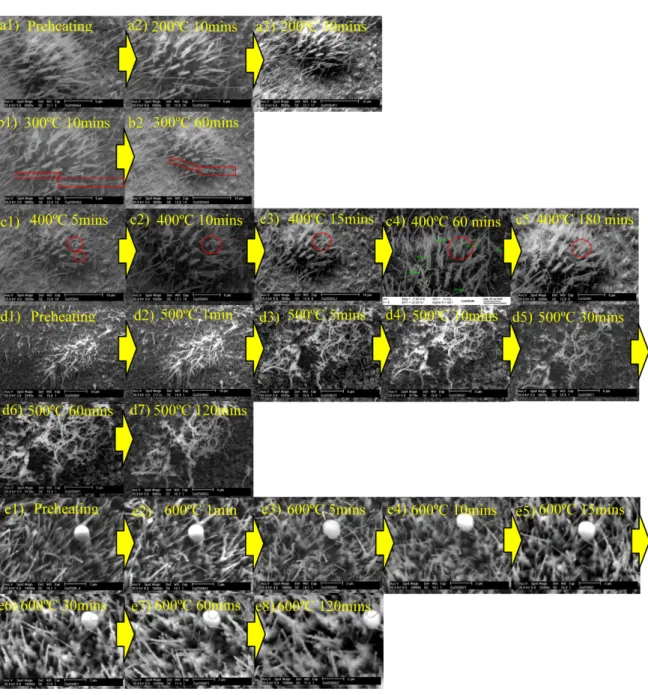
Fig. 1 shows a series of SEM micrographs for as-synthesized copper oxide NWs and morphology after annealing at various temperatures in N2 ambient. SEM pictures shows that the surface of the copper plate was completely covered by a dense array of uniform copper oxide NWs. The diameters for the as grown copper oxide wires are in between ~50 to ~500 nm. They are formed on the top surface of the layer peeling off from copper plates. The bases of the copper oxide wires are consist of the copper oxide granules. The peel-off effect may due to the strain induced when the formation of copper oxide granule. As shown in Fig. 1, the thickness of the peeled off layer is about 10µm, the wires are grown from the granular oxide layer.
For copper oxide NWs heated in N2 ambient at 200ºC, no damage and collapse of the NWs have been observed. At 300ºC, it starts to reach the softening point of the copper oxide NWs where the NWs with diameter less than 100 nm start to bend due to the thermal shock. The strength of the NWs starts to fail in supporting themselves. The red box in Fig. 2 (b1 and b2) clearly shows the change of the straight wires to curve shape after 60 minutes of heating. As the wires were abruptly heated to 400ºC for 5 minutes, the wires with bigger diameters (~300 nm) started to collapse (As shown in the red circles in Fig. 2 (c1)). Some crystal defects might be induced to the wires due to thermal shock. The continuous annealing process didn’t cause any further bending and collapse of the same wires. Therefore, it is suggested that the sintering process take place to cover up the defect and strengthen the copper oxide wires after the initial bending. As the thermal shock of 500ºC was applied to the sample (by inserting the samples instantly into the center of the tube), almost all copper oxide wires were skewed, distorted and collapsed after 5 minutes of heating. The failure point of NWs has been achieved due to both the combination of thermal shock with sufficient high temperature (500ºC).
Fig. 1. SEM pictures for the as-grown CuO NWs
~10µm
Proc. of SPIE Vol. 7493 749346-2
A new sample was undergoing an annealing process with temperature of 600ºC. The abrupt increase in the temperature was avoided this time by inserting the sample slowly into the tube as mentioned in experimental method. The collapse due to the thermal shock was not observed this time. It was found that copper oxide NWs under the slow-heating annealing process can withstand higher temperature. Those NWs with the same diameters which would have collapsed at 500°C still maintaining the self-supporting capability.
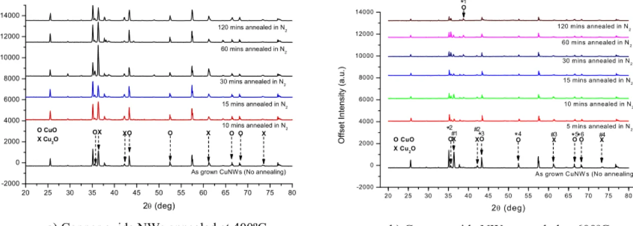
XRD analyses were also been carried out on the pre and post-annealed samples at 400ºC and 600ºC. Fig. 3 a) and b) shows the XRD spectra of the copper oxide NWs after annealed at 400ºC and 600ºC respectively. Basically, the synthesis processes formed both the CuO and Cu2O crystalline materials as shown in the XRD spectra with the marking of “O” and “X” respectively. There is no significant change on the intensity of diffraction peaks for both CuO and Cu2O after annealing in N2 at 400ºC. Some non-labeled peaks from the silver paste and Al2O3 substrates are also shown in the same spectra.
Fig. 2. SEM images for copper oxide NWs annealed in N2 ambient at 200, 300, 400, 500 and 600ºC.
Proc. of SPIE Vol. 7493 749346-3
For copper oxide NWs annealed at 600ºC in N2 ambient, intensities of Cu2O peaks (#1, #2, #3 and #4) gradually diminished. The intensity of a CuO peak indicated as “*1” started to appear upon annealing in N2 ambient. This suggests that new form of CuO structure has been created and it might be developed from the diminishing of Cu2O structure after the sample was heated for 120 minutes. Though, the reduction of CuO peaks intensities labeled with “*3, *4, *5 and *6 may because of the deterioration and collapse of the existing CuO NWs after prolong heating in N2 ambient.
4. CONCLUSIONS
Thermal property of copper oxide NWs in N2 ambient has been studied. The failure process of the free-standing copper oxide NWs has been observed under excessive thermal environment. The copper oxide NWs are able to withstand annealing temperature of 600ºC for two hrs if no sudden and abrupt temperature increment. The thermal shock will destroy the wires easily even at temperature as low as 300ºC. XRD results show that the Cu2O structures ware gradually diminished if annealed at 600ºC. All these information are important by the time when copper oxide is ready to be integrated into a standard CMOS circuit.
5. ACKNOWLEDGMENTS
This work has been supported in part by Science fund (03-01-02-SF0076) and GUP (UKM-GUP-BTT-0726-179) 6. REFERENCES
1. M. K. Wu, J. R. Ashburn, C. J. Torng, P. H. Hor, R. L. Meng, L. Gao, Z. J. Huang, Y. Q. Wang, and C. W. Chu, "Superconductivity at 93K in a new mixed-phase Y-Ba-Cu-O compound system at ambient pressure," Physical
Review Letters. 58(9), 908-910 (1987).
2. V. R. Katti, A. K. Debnath, K. P. Muthe, M. Kaur, A. K. Dua, S. C. Gadkari, S. K. Gupta, and V. C. Sahni, "Mechanism of drifts in H2S sensing properties of SnO2:CuO composite thin film sensors prepared by thermal evaporation," Sensors Actuators B. 96, 245-252 (2003).
3. F. R. N. Nabarro and J. P. J, Growth of crystal whiskers, in Growth and perfection of crystal growth R.H. Daremus, R.B. W, and T. D, Editors. 1958, Wiley: New York.
4. Y. W. Zhu, T. Yu, F. C. Cheong, X. J. Xu, C. T. Lim, V. B. C. Tan, J. T. L. Thong, and C. H. Sow, "Large-scale synthesis and field emission properties of vertically oriented CuO nanowire films," Nanotechnology. 16, 88-92 (2005).
5. L. Shenzhong, Z. Hui, J. Yujie, and D. Yang, "CuO nanodendrites synthesized by a novel hydrothermal route,"
Nanotechnology. 15, 1428-1432 (2004). 20 25 30 35 40 45 50 55 60 65 70 75 80 -2000 0 2000 4000 6000 8000 10000 12000 14000 O CuO X Cu2O
As grown CuNWs (No annealing) 120 mins annealed in N2 60 mins annealed in N2 30 mins annealed in N2 15 mins annealed in N2 10 mins annealed in N2 Off se t Inte n sity (a .u.) 2θ (deg) O X OX O X O O X
Fig. 3. XRD spectra for copper oxide NWs annealed at 400 and 600ºC.
a) Copper oxide NWs annealed at 400ºC b) Copper oxide NWs annealed at 600ºC
20 25 30 35 40 45 50 55 60 65 70 75 80 -2000 0 2000 4000 6000 8000 10000 12000 14000 6 * #4 3 # 2 # 1 # *3 *4 *5 2 * O CuO X Cu2O O 5 mins annealed in N2 120 mins annealed in N2 60 mins annealed in N2 30 mins annealed in N2 15 mins annealed in N2 10 mins annealed in N2 O ffse t In ten si ty ( a. u. ) 2θ (deg)
As grown CuNW s (No annealing) O
X
OX O X O O X
*1
Proc. of SPIE Vol. 7493 749346-4
6. Y.-k. Su, C.-m. Shen, H.-t. Yang, H.-l. Li, and H.-j. Gao, "Controlled synthesis of highly ordered CuO nanowire arrays by template-based sol-gel route," Trans. Nonferrous Met. Soc. China. 17(4), 783-786 (2007).
7. J. P. Liu, X. T. Huang, Y. Y. Li, K. M. Sulieman, X. He, and S. F. G, "Self-Assembled CuO Monocrystalline Nanoarchitectures with Controlled Dimensionality and Morphology," Cryst. Growth Des. 6, 1690-1696 (2006). 8. X. Wang, G. Xi, S. Xiong, Y. Liu, B. Xi, W. Yu, and Y. Qian, "Solution-phase synthesis of single-crystal CuO
nanoribbons and nanorings," Cryst. Growth Des. 7(5), 930-934 (2007).
9. W. Wang, Y. Zhan, X. Wang, Y. Liu, C. Zheng, and G. Wang, "Synthesis and characterization of CuO nanowhiskers by a novel one-step, solid-state reaction in the presence of a nonionic surfactant," Materials Research
Bulletin. 37(6), 1093-1100 (2002).
10. C. F. Dee, M. Yahaya, M. M. Salleh, and B. Y. Majlis. "Synthesis and characterization of CuO nanowires," Proc. IEEE International Conference on Semiconductor Electronics. 286-289 (2006).
11. Y. L. Liu, L. Liao, J. C. Li, and C. X. Pan, "From copper nanocrystalline to CuO nanoneedle array: Synthesis, growth mechanism, and properties," J. Phys. Chem. C. 111, 5050-5056 (2007).
12. W. X. Zhang, X. G. Wen, and S. H. Yang, "Controlled reactions on a copper surface: Synthesis and characterization of nanostructured copper compound films," Inorg. Chem. 42, 5005-5014 (2003).
13. W.-T. Yao, S.-H. Yu, Y. Zhou, J. Jiang, Q.-S. Wu, L. Zhang, and J. Jiang, "Formation of Uniform CuO Nanorods by Spontaneous Aggregation; Selective Synthesis of CuO, Cu2O, and Cu Nanoparticles by a Solid Liquid Phase Arc Discharge Process," The Journal of Physical Chemistry B. 109(29), 14011-14016 (2005).
14. W. Zhang, S. Ding, Z. Yang, A. Liub, Y. Qian, S. Tang, and S. Yang, "Growth of novel nanostructured copper oxide (CuO) films on copper foil," J of Crys. Growth. 291(2), 479-484 (2006).
15. K. Zhou, R. Wang, B. Xu, and Y. Li, "Synthesis, characterization and catalytic properties of CuO nanocrystals with various shapes," Nanotechnology. 17, 3939-3943 (2006).
16. L. Liao, Z. Zhang, B. Yan, Z. Zheng, Q. L. Bao, T. Wu, C. M. Li, Z. X. Shen, J. X. Zhang, H. Gong, J. C. Li, and T. Yu, "Multifunctional CuO nanowire devices: p-type field effect transistors and CO gas sensors,"
Nanotechnology. 20, 085203-085208 (2009).
17. H. Jansen, M. d. Boer, R. Legtenberg, and M. Elwenspoek, "The black silicon method: a universal method for determining the parameter setting of a fluorine-based reactive ion etcher in deep silicon trench etching with profile control," J. Micromech. Microeng. 5, 115-120 (1995).
Proc. of SPIE Vol. 7493 749346-5