Investigation of the effect of different oxygen partial pressure to LaAlO
3
thin
film
properties and resistive switching characteristics
Kou-Chen Liu
a,⁎
, Wen-Hsien Tzeng
b, Kow-Ming Chang
b,c, Jiun-Jie Huang
b, Yun-Ju Lee
d, Ping-Hung Yeh
d,
Pang-Shiu Chen
e, Heng-Yuan Lee
f, Frederick Chen
f, Ming-Jinn Tsai
fa
Institute of Electro-Optical Engineering, Chang Gung University, Tao-Yuan 33302, Taiwan, ROC
b
Institute of Electronics, Department of Electronics Engineering, National Chiao Tung University, HsinChu 30010, Taiwan, ROC
c
Department of Electronic Engineering, I-Shou University, No. 1, Sec. 1, Syuecheng Rd., Kaohsiung 840, Taiwan, ROC
d
Department of Physics, Tamkang University, Tansui 251, Taiwan, ROC
eDepartment of Material Science and Engineering, Minghsin University of Science and Technology, Hsinchu 340, Taiwan, ROC f
Electronics and Optoelectronics Research Laboratory, Industrial Technology Research Institute, Hsinchu 310, Taiwan, ROC
a b s t r a c t
a r t i c l e i n f o
Available online 4 May 2011 Keywords:
Lanthanum aluminate Resistive switching Switching memory Oxygen partial pressure LaAlO3
Pulsed laser deposition
The pulsed laser deposition and growth of a high-k dielectric lanthanum aluminate LaAlO3(LAO) thinfilm on
indium tin oxide/glass substrate at different oxygen partial pressure was studied. Based on the pulsed laser deposition growth mechanism, we explain how a difference in the oxygen partial pressure influences the surface roughness, formation of an interfacial layer, and the transparent resistive switching characteristics of LAO thinfilms. The micro-structure and oxygen concentration difference inside LAO thin films may be the main reason for the difference in electrical and resistive switching properties. Films grown at higher oxygen partial pressure displayed more reliable resistive switching performance, due to the formation of the interfacial layer and a lower concentration of oxygen vacancies. The interfacial layer serves as a good oxygen reservoir and the involvement of more oxygen ions ensures the switching reliability. The migration of oxygen ions between the interfacial layer and the LAOfilm under applied bias may be the switching mechanism.
© 2011 Elsevier B.V. All rights reserved.
1. Introduction
The high demand for nonvolatile memory (NVM) with low power consumption, high density, and compatibility with conventional complementary metal oxide semiconductor (CMOS) technology has led to increased research. As a result, resistive random access memory (RRAM), which is based on the concept of resistance switching (RS), has emerged as one of the prime candidates for next generation NVM
[1–3]. Several materials have been shown to exhibit RS characteristics, including transition metal oxide[4–6], perovskite oxides[7–9], and some organic materials[10]. Various models such as thefilamentary model [11,12] and the charge trapping model [13,14] have been proposed to explain the RS mechanism. Most of these materials show polycrystalline structures, and the existence of the grain boundaries may facilitate the formation of the conducting filaments and determine the electrical properties[15]. In recent years, amorphous materials have also attracted attention since they are free from grain boundaries which improve film uniformity and avoid detrimental pad-to-pad variations in switching characteristics, in contrast to polycrystalline cells. However, the resistive switching mechanism in
amorphousfilms might be different from that in polycrystalline films due to the absence of these grain boundary defects in amorphous thin films.
In this study, we investigate the use of amorphous LaAlO3(LAO)
thinfilms for RRAM devices. The ternary oxide LaAlO3, is one of the
materials that has been identified by the semiconductor industry as a potential replacement for SiO2in gate dielectric layers. It has a high
dielectric constant of 25[16]and has large band offsets (over 2 eV) with silicon[17]. Furthermore, the thinfilm of LAO is amorphous at temperatures up to 800 °C[18], the band gap is predicted to be 6.2 eV
[19], and it is theoretically thermally stable in contact with silicon at up to 1000 °C[20]. Since the LAO thinfilm exhibits reliable RS properties, it is a good choice for 1T1R integration applications. However, the use of a lanthanum-based dielectric layer for the RRAM applications has not received great attention. In lanthanum-based films, the oxygen vacancy density is critical for determining the resistance values. The influence of oxygen partial pressure during pulsed laser deposition (PLD) on the thin film morphology and resistive switching properties of LAO is the subject of our study. 2. Experimental method
The PLD process was used to deposit the LAOfilms using an LAO target as the resistive layer of transparent RRAM (T-RRAM) device on
⁎ Corresponding author.
E-mail address:[email protected](K.-C. Liu).
0040-6090/$– see front matter © 2011 Elsevier B.V. All rights reserved. doi:10.1016/j.tsf.2011.04.205
Contents lists available atScienceDirect
Thin Solid Films
an indium tin oxide (ITO)/glass substrate. A KrF excimer laser (λ=248 nm) was used as the light source for PLD with a pulse duration of 25 ns, a repetition rate of 3 Hz, and laser energy of 500 mJ. The distance from the target to the substrate was 10 cm and the target rotation rate was 5 rpm. The ambient oxygen pressure, which is the most important parameter of the PLD process, was varied, taking values of 0.93, 1.87, and 3.73 Pa. We use ITO as a top electrode (TE). A 100 nm ITOfilm was deposited using the dc sputter system using a shadow mask with a diameter of 1200μm. The electrical characterization was carried out using an Agilent 4156C semiconductor parameter analyzer (SPA) at room temperature. The surface morphology, LAOfilm thickness and chemical composition of LAO thinfilms was characterized by atomic force microscopy (AFM), a surface profiler and X-ray photoelectron spectroscopy (XPS). Cross-sectional high resolution transmission electron microscopy (HR-TEM) was employed to examine the micro-structure. The currentflow from the top to the bottom electrode was defined as a positive sweep.
3. Results and discussion
The surface roughness of LAO thin film with oxygen partial pressure of 0.93 (L1), 1.87 (L2), and 3.73 (L3) Pa was measured by AFM. The root mean square (RMS) surface roughness of L1, L2, and L3 samples was about 3.66, 4.00, and 4.38 nm, respectively, as shown in
Fig. 1(a)–(c). The thicknesses of the L1, L2, and L3 samples were about 25, 28, and 40 nm, as measured using the surface profiler and TEM analysis. The PLD process parameter such as oxygen pressure[21]
or substrate temperature [22], can influence the thin film growth mechanism and the nucleation reaction—the LAO thin film thickness and surface roughness increased linearly with oxygen content. This increase may be related to some physical properties of thin film growth conditions. The cross sectional structures of the stacked ITO/LAO/ITO devices were characterized by HR-TEM, as shown in
Fig. 2(a)–(c). A very clear interfacial layer (IL) with a rougher surface between the ITO substrate and the LAO film deposited in the L3 sample is clearly observed, while no IL can be observed in L1. This indicates that LAO thinfilm deposition at a higher oxygen pressure aids the formation of the IL. The three LAO samples were all in the amorphous phase due to the high crystallization temperature of about 800 °C[18].
To explain how the oxygen pressure influences the thin film growth during the PLD process, we need to examine the mechanism of the PLD fabrication process. The PLD-deposited thinfilm properties show a high correlation with the conditions in the chamber. The oxygen gas has two effects expected to influence the film formation. It alters the evaporated plume length, and provides a highflux of background gas particles bombarding the surface during the deposition. The evaporated plume is a critical factor to determine the deposited thinfilm quality during PLD. According to Dyer et al.[23], the deposited thinfilm quality was influenced by the specific effect of the plume length and ambient pressure. The plume length L and the oxygen pressure Pofollow Lα
(E/Po)1/3γ, where E is the laser-pulse energy, andγ is the ratio of specific
heats of the elements in the plume. From the above equation, high oxygen pressure has a corresponding shorter plume length L. They mentioned that as the target-to-substrate distance is located beyond the plume length L, the concentration of smaller clusters decreases and larger clusters appear, indicating that with a longer transfer time, the clusters merge via reaction [24]. Therefore, the vaporized species undergo more collisions and form larger clusters during transformation from plume to the substrate surface. Ionized atomic oxygen is quite reactive and tends to interact easily with the vaporized species. A continuous source of atomic oxygen can contribute on oxygen activity and arrival adatoms to the substrate surface, thus leading to higher deposition rate and thicker LAO thinfilm. The quality of the vacuum is a major practical consideration for the determination of the deposition rate[25,26]. Therefore, the thicker thinfilm was observed under the
same deposition time as shown inFig. 2. The deposition rate alternation may lead to different thinfilm nucleation and growth mechanism. For a high oxygen pressure circumstance, the vaporized species tend to form clusters before arriving at the substrate surface. Large clusters have the additional effect of decreasing the surface diffusion coefficient of the adsorbed vapor atoms, therefore, the adhesion of the ejected matter is poor, the shape size growth follows a random distribution, and a rougher
a
b
c
Fig. 1. AFM images of the LAOfilms grown with oxygen partial pressures of (a) 0.93, (b) 1.87, and (c) 3.73 Pa.
surface can be expected. Another possible reason for the increase in surface roughness with increasing oxygen pressure may be attributed to an increased particulate formation in the laser plume[27]. In addition, the atomic oxygen may be kicked or impinged onto the substrate surface, which causes growth of the interfacial layer during thinfilm deposition.
Fig. 3shows the XPS spectra of the La 3d core level electrons. The peak binding energy of the La 3d core level electron increases with the
increase in oxygen pressure from 0.93 to 3.73 Pa; this can be attributed to highly oxidized of the LAOfilm. Further, fewer structural defects are introduced. The Al 2p core level electron shifts from 72 to 74 eV; this corresponds to a peak binding energy shift from near metal Al0+to the oxidized Al3+spectra. Xiang et al.[28]claimed that when
LAOfilm is deposited under a high oxygen pressure of 10− 1Pa, the
kinetic and internal energy of theflying particles is easily lost due to frequent collisions and reactions between the evaporated particles and oxygen. Above 2 × 10− 3Pa, the stoichiometric ratio of La, Al, and O in the deposited LAOfilms is maintained at around 1:1:3, otherwise the oxygen content decreases with decreasing oxygen pressure. The leakage current density of LAO thinfilms, which decreases gradually with the increase in oxygen pressure at a certain given electricfield value, corresponds with the XPS analysis. The XPS results confirm that at high oxygen pressure, the atomic oxygen compensates for the oxygen deficiency of vaporized species by collision or reaction. The result is a stronger binding energy of the oxidized peak and less defects in the LAO thinfilm. For resistive memory applications, the LAO thinfilm property must be well controlled during PLD fabrication by modulating the oxygen pressure.
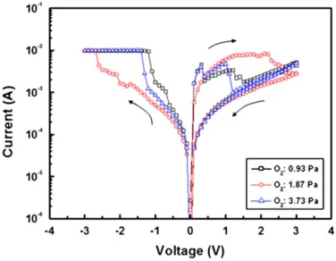
The forming process is needed in the beginning to trigger the RS properties, and the L3 samples exhibit the largest forming voltage than the others. This may be due to the thicker thickness and/or less oxygen deficiency on L3 samples. After the forming process, three
5 nm
a
5 nm
b
c
5 nm
Fig. 2. High resolution cross-sectional TEM images of the LAOfilms grown with oxygen partial pressures of (a) 0.93, (b) 1.87, and (c) 3.73 Pa.
Fig. 3. XPS spectra of the La 3d core-level electrons of the three samples.
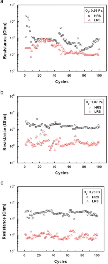
devices exhibited bipolar RS behavior, and the RS from the low resistance state (LRS) to high resistance state (HRS) can be realized with positive voltages (clockwise loop). To evaluate the memory performance of the ITO/LAO/ITO devices, the endurance characteris-tics were measured, as shown inFig. 4.Fig. 5(a)–(c) compares the endurance characteristics of the three LAO devices. During the 100
consecutive switching cycles, several switching-failure cycles are observed on the L1 devices. The resistance values in both states are distinguishable on the L3 devices. The average values of the resistance ratio measured at a bias voltage of 0.1 V was about 4.7, 9.7, and 26.7 for the L1, L2, and L3 respectively. The ratio is similar to amorphous Ga2O3 films using the PLD process [29]. As non-volatile memory
device application, RRAM devices usually require a large ratio between HRS and LRS to have a high signal-to-noise ratio. The distinct bipolar RS properties of the three samples may be due to the difference in composition of LAO thinfilms and the micro-structure at the LAO/ITO (BE) interface.
Two factors influence the stable RS characteristics: the structural difference and composition differences. For the former, we can clearly observe fromFig. 2(a) and (c), there is an additional IL at the LAO/ITO (BE) interface of L2 and L3 samples, but not L1. The IL serves as a reservoir for oxygen ions under the applied bias. As a negative voltage is applied to the top electrode, oxygen ions move toward the interfacial layer, and the state is switched to LRS. During the operation, the oxygen ions can rest inside this IL, contributing to a large conducting current. When a positive voltage is applied, the oxygen ions move back to the LAO thinfilm and the state switches to HRS. The oxygen ion migration between the IL and LAO thinfilms dominates the state to LRS or HRS. The resistance value level is determined by the number of oxygen ions involved, this is the second factor. Under the identical current compliance of 10 mA, the L3 sample extracts more oxygen ions due to oxygen defects deficiency, as shown inFig. 3. This indicates that higher oxygen content can be involved for the RS characteristics on L3 samples, compared to the L1 samples. The involvement of more oxygen ions ensures the reliability of the switching behaviors, especially during the LRS to HRS operation. This improves the RS stability. This may also explain why L2 samples with an IL at the LAO/ITO interface still show several unreliable switching characteristics. Although the ITO electrode can also serve as an oxygen reservoir controlling RS characteristics, the observed RS properties are poor and the high and low resistance values are unstable from cycle to cycle, like the L1 samples shown inFig. 5(a). Random fluctuations of the high and low resistance values for L1 samples cause severe degradation and data read-out errors, resulting in unreliable memory performance. Physical thickness difference of the three samples was not the dominate factor for the RS, because the effective thickness for the RS operation may depend on material and is difficult to be expected. We also tested the opposite RS characteristic by sweeping the counter-clockwise loop (positive bias for HRS to LRS and negative one for LRS to HRS) on the three samples; the three devices can also be switched to HRS using a negative bias. However, the RS properties are quite poor compared to the clockwise direction (not shown here). Therefore, the existence of the IL is essential for a reliable RS operation, like the La0.7CaMnO3 (LCMO)/TiOx reported
by Liu et al.[30]. Based on these observations, we believe that the presence of the IL is responsible for the stable RS characteristics of the LAO thin films. Also, a thin film with lower oxygen vacancy concentration displays better high to low resistance ratio RS properties because more oxygen ions are involved in the switching process. 4. Conclusion
The transparent ITO/LAO/ITO sandwich structures were fabricated and the resistive switching characteristics of LAO T-RRAM grown at different oxygen partial pressures using pulsed laser deposition were investigated. We explain how different oxygen partial pressures influence the thin film morphology based on the thin film growth mechanism. The LAOfilms grown at higher oxygen partial pressure provide lower leakage current, and a more stable high to low resistance ratio. The interfacial layer serves as a good reservoir for oxygen ions. The migration of the ions between the interfacial layer and LAOfilm may be the switching mechanism involved. Further work is needed to study
a
b
c
Fig. 5. The resistance values of both ON and OFF-state at 0.1 V of LAO-based transparent memory grown with oxygen partial pressure of (a) 0.93, (b) 1.87, and (c) 3.73 Pa.
how the difference in the oxygen content of LAOfilms influences the switching reliability under different temperatures and how to the ITO electrode instability can be overcome.
References
[1] I.G. Baek, M.S. Lee, S. Seo, M.J. Lee, D.H. Seo, D.-S. Suh, J.C. Park, S.O. Park, H.S. Kim, I.K. Yoo, U.-In. Chung, J.T. Moon, IEDM Tech. Dig, 2004, p. 587.
[2] T. Fujii, M. Kawasaki, A. Sawa, H. Akoh, Y. Kawazoe, Y. Tokura, Appl. Phys. Lett. 86 (2005) 012107.
[3] R. Waser, M. Aono, Nat. Mater. 6 (2007) 833.
[4] C. Rohde, B.J. Choi, D.S. Jeong, S. Choi, J.S. Zhao, C.S. Hwang, Appl. Phys. Lett. 86 (2005) 262907.
[5] S. Kim, I. Byun, I. Hwang, J. Kim, J. Choi, B.H. Park, S. Seo, M.J. Lee, D.H. Seo, D.S. Suh, Y.S. Joung, I.K. Yoo, Jpn. J. Appl. Phys. 44 (2005) L345.
[6] K.C. Liu, W.H. Tzeng, K.M. Chang, Y.C. Chan, C.C. Kuo, C.W. Cheng, Microelectronic Reliab. 50 (2010) 670.
[7] N. Das, S. Tsui, Y.Y. Xue, Y.Q. Wang, C.W. Chu, Phys. Rev. B 78 (2008) 235418. [8] J.W. Park, M.K. Yang, K. Jung, J.K. Lee, IEEE Trans. Electron. Dev. 55 (2008) 782. [9] C.Y. Liu, P.H. Wu, A. Wang, W.Y. Jang, J.C. Young, K.Y. Chiu, T.Y. Tseng, IEEE Electron
Dev. Lett. 26 (2005) 351.
[10] X.N. Liu, Z.Y. Ji, D.Y. Tu, L.W. Shang, J. Liu, M. Liu, C.Q. Xie, Org. Electron. 10 (2009) 1191.
[11] M. Liu, Z. Abid, W. Wang, X. He, Q. Liu, W. Guan, Appl. Phy. Lett. 94 (2009) 233106. [12] G.S. Park, X.S. Li, D.C. Kim, R.J. Jung, M.J. Lee, S. Seo, Appl. Phy. Lett. 91 (2007)
222103.
[13] L. Goux, J.G. Lisoni, T. Gille, K. Attenborough, D.J. Wouters, ECS Lett. 11 (2008) H245.
[14] A. Chen, S. Haddad, Y.C. Wu, IEEE Electron Dev. Lett. 29 (2008) 38.
[15] S. Kim, H. Moon, D. Gupta, S. Yoo, Y.K. Choi, IEEE Trans. Electron Dev. 56 (2009) 696.
[16] B.-E. Park, H. Ishiwara, Appl. Phys. Lett. 79 (2001) 806.
[17] L.F. Edge, D.G. Schlom, S.A. Chambers, E. Cicerrella, J.L. Freeouf, B. Hollander, J. Schubert, Appl. Phys. Lett. 84 (2004) 726.
[18] M. Suzuki, T. Yamaguchi, N. Fukushima, M. Koyama, J. Appl. Phys. 103 (2008) 034118.
[19] Y.Y. Mi, Z. Yu, S.J. Wang, P.C. Lim, Y.L. Foo, A.C.H. Huan, C.K. Ong, Appl. Phys. Lett. 90 (2007) 181925.
[20] K.L. Ovanesyan, A.G. Petrosyan, G.O. Shirinyan, C. Pedrini, L. Zhang, Opt. Mater. 10 (1998) 291.
[21] B. Ali, A.K. Rumaiz, A. Ozbay, E.R. Nowak, S.I. Shah, Solid state commun. 149 (2009) 2210.
[22] C.V. Ramana, R.J. Smith, O.M. Hussain, C.M. Julien, Mater. Sci. Eng. B 111 (2004) 218.
[23] P.E. Dyer, A. Issa, P.H. Key, Appl. Phys. Lett. 57 (1990) 186.
[24] Y. Nishikawa, K. Tanaka, Y. Yoshida, Nippon Kinzoku Kaishi 55 (1991) 581. [25] S.S. Kim, B.-T. Lee, Thin Solid Films 446 (2004) 307.
[26] X.B. Lu, Z.G. Liu, X. Zhang, R. Huang, H.W. Zhou, X.P. Wang, B.-Y. Nguyen, J. Phys. D: Appl. Phys. 36 (2003) 3047.
[27] L.C. Chen, in: D.B. Chrisey, G.K. Hubbler (Eds.), Pulsed Laser Deposition of Thin Films, Wiley, New York, 1994, p. 115.
[28] W. Xiang, H. Lu, L. Yan, H. Guo, L. Liu, Y. Zhou, G. Yang, J. Jiang, H. Cheng, Z. Chen, J. Appl. Phys. 93 (2003) 533.
[29] X. Gao, Y. Xia, J. Ji, H. Xu, Y. Su, H. Li, C. Yang, H. Guo, J. Yin, Z. Liu, Appl. Phy. Lett. 97 (2010) 193501.
[30] X.J. Liu, X.M. Li, Q. Wang, W.D. Yu, R. Yang, X. Cao, X.D. Gao, L.D. Chen, Solid State Commun. 150 (2010) 137.