Improvement of Crystalline and Photoluminescence of Atomic Layer
Deposited
m‑Plane ZnO Epitaxial Films by Annealing Treatment
S. Yang,
#B. H. Lin,
#,†C. C. Kuo,
#H. C. Hsu,
‡,¶W.-R. Liu,
#,†M. O. Eriksson,
§P.-O. Holtz,
§C.-S. Chang,
#C.-H. Hsu,*
,†,#and W. F. Hsieh*
,#,‡#Department of Photonics & Institute of Electro-Optical Engineering, National Chiao Tung University, Hsinchu 30050, Taiwan †Division of Scientific Research, National Synchrotron Radiation Research Center, Hsinchu 30076, Taiwan
‡Department of Photonics and Advanced Optoelectronic Technology Center, National Cheng Kung University, Tainan 70101,
Taiwan
¶Research Center for Energy Technology and Strategy, National Cheng Kung University, Tainan 70101, Taiwan §Department of Physics, Chemistry and Biology (IFM), Linköping University, Linköping, Sweden
ABSTRACT: Monocrystalline m-plane ZnO epitaxial films withflat surface morphology were grown on m-plane sapphire by using atomic layer deposition. X-ray diffraction and transmission electron microscopy measurements verify not only the in-plane epitaxial relationship of the as-grownfilms as (101̅0)⟨0001⟩ZnO||(101̅0)⟨1̅21̅0⟩Al2O3 but also the absence of domains with undesirable orientations, which are generally obtained in the m-plane ZnO films grown by other methods. Experimental results indicate that the basal plane stacking fault (BSF) is the dominant structural defects that contribute to the
emission at 3.31 eV in m-plane ZnOfilms. Exactly how thermal annealing affects the structural and optical properties of ZnO epi-films was also investigated. Additionally, based on time-resolved photoluminescence at 5 K, the decay time of BSF related emission and near-band-edge (NBE) emission were determined. Results of this work further demonstrated that the decay time of NBE emission increases with a higher annealing temperature, accompanied by an improvement in crystal structure.
■
INTRODUCTIONZnO based materials have been widely investigated owing to their photonic applications. The advantages of ZnO including high stability, UV-excitonic emission at room temperature (RT), low manufacturing costs, and nontoxicity make it a highly promising material for UV-light emitting devices (LEDs) and an alternative to conventional GaN-based materials. Recent studies have demonstrated the feasibility of fabricating blue LEDs by using polar ZnO.1,2 c-Plane sapphire is extensively adopted as a substrate to grow ZnO epitaxialfilms of excellent quality and at an acceptable cost. Nevertheless, strong spontaneous polarization and piezoelectric polarization at the interfaces of ZnO based heterostructures induce a large internal electricfield along the c-axis, resulting in the quantum-confined Stark effect and ultimately a spectral red-shift and significant decrease in luminous efficiency. To avoid this problem, considerable efforts have been made to increase luminous efficiency by taking advantage of the nonpolar m-plane orientated ZnO layers through several growth methods, including molecular beam epitaxy (MBE),3−6 metal organic chemical vapor deposition (MOCVD),7,8 and pulsed laser deposition (PLD).9,10 Unfortunately, fabricating m-plane ZnO epi-films with high structural perfection and smooth surface morphology is still quite difficult. A common problem is the coexistence of minor domains with (101̅3),3,6,7 (0002),6 or
(112̅2)6 orientations. In particular, (101̅3) oriented domains are often observed and difficult to eliminate. Moreover, the surface morphologies of the deposited m-plane ZnOfilms on foreign substrates often exhibit striped features that are elongated along a direction either parallel or normal to the ZnO c-axis, depending on growth conditions.7,8,11 These features strongly hamper the applicability of ZnO-based heterostructures. Different from other growth methods, the growth mechanism of atomic layer deposition (ALD) relies on the sequential self-terminated chemical reactions, leading to layer-by-layer growth with the advantages of accurate thickness control, high uniformity, high reproducibility, high covering ratio, and low growth temperature. Despite the success in growing epitaxial m-plane ZnOfilms without minor domains on a m-plane sapphire by ALD,12 the crystalline quality of epitaxial films must be further improved, and the correlation between structural and optical properties should be explored in depth.
In this work, m-plane oriented ZnO epitaxialfilms are grown with a single crystallographic orientation and smooth surface morphology by using the ALD method. Thermal annealing Received: March 21, 2012
Revised: August 6, 2012 Published: August 21, 2012
treatment allows us to further improve the crystallinity and morphology of these m-plane ZnO layers. The epitaxial relationship (101̅0)⟨0001⟩ZnO||(101̅0)<1̅21̅0>Al2O3with a nearly perfect domain match along the [12̅10]ZnO direction is also
confirmed. Additionally, experimental results identify basal plane stacking faults (BSFs) with a density of about∼106cm−1
as the major defects leading to the broad emission around 3.31 eV in the photoluminescence (PL) spectra. According to time-resolved photoluminescence (TR-PL) results, lifetime of the D0X emission increases with an increasing thermal annealing
temperature. For the sample annealed at 800°C, its D0X and BSF emission have life times about 58 and 500 ps, respectively. Based on these results, how the specific growth mechanism of the ALD method influences the growth of m-plane ZnO on the m-plane sapphire is discussed.
■
EXPERIMENTAL SECTIONPrior to ZnO deposition, m-plane (101̅0) oriented sapphire was cleaned by sequential D.I. water/acetone/D.I. water rinse for 5 min/5 min/5 min, followed by blow drying with N2 gas. A clean sapphire substrate was loaded into the ALD reactor (SYSKEY Ltd., Taiwan), followed by heating to 200°C and maintaining that temperature for 30 min. Diethylzinc (DEZn with a chemical formula of Zn(C2H5)2 supported by SAFC) and H2O (D. I. water of 18 MΩcm) kept in reservoirs at 25 °C were used as zinc and oxygen precursors, respectively. The growth cycle consisted of precursor exposures and N2 purge following the sequence of DEZn/N2/H2O/N2 with corresponding durations of 5s/15s/5s/15s. Precursor exposure includes introducing and depositing the precursor. DEZn and H2O have a vapor pressure of about 7 and 17 Torr (∼933 and ∼2266 Pa), respectively, at RT. Precursors were introduced into the chamber by opening the valves to the precursor reservoirs for 200 ms; no carrier gas was used. The chamber was then isolated and maintained at a pressure of 1−2 Torr (133−166 Pa) for 5 s to facilitate the chemical reaction at the sample surface. High purity N2 gas (4N) was subsequently introduced with aflow rate of 500 sccm, accompanied by chamber evacuation for 10 s to purge the reaction chamber. Continuous pumping for 5 s after termination of the N2flow yields a chamber pressure of about 1× 10⁻²Torr (∼1.3 Pa) prior to another run of precursor introduction. All of the samples underwent 400 growth cycles, followed by thermal annealing at temperatures varying from 400 to 800°C for 1 h in pure oxygen at atmosphere of 1 atm. X-ray diffraction (XRD) measurements were conducted using a four-circle diffractometer at the beamline BL13A of the National Synchrotron Radiation Research Center (Hsinchu, Taiwan) with an incident wavelength of 1.025 Å. Two pairs of slits were used between the sample and a NaI scintillation detector, yielding a typical resolution higher than 1× 10⁻³Å−1. Surface morphology and roughness of the ZnO films were measured by a Veeco Innova Scanning Probe Microscope. Next, the structural defects of the ZnO thinfilms were analyzed using transmission electron microscopy (TEM). TEM specimens with a thickness∼80 nm were prepared by using a focused ion beam (FEI Helios 400S). High resolution TEM (HR-TEM) images were captured by using the JEOL JEM-2100F TEM with accelerating voltage 200 kV, and the selected area electron diffraction (SAED) patterns were taken at the ZnO/sapphire interface with afield of view∼130 nm. Additionally, dark field images were taken by using a FEI TECNAI G2 20 TEM with an accelerating voltage of 200 kV, camera length of 300 mm, and objective aperture size of 10μm. For transient PL measurements, the third harmonic (λexc = 266 nm) obtained from a femtosecond Ti:sapphire laser with a pulse width of 150 fs and a repetition rate of 76 MHz was used as an excitation source. Moreover, the luminescence signal was dispersed by a 0.3 m monochromator and recorded by a UV sensitive streak camera (Hamamatsu C5680), yielding a spectral resolution of about 1 meV and temporal resolution better than 10 ps. All of the PL spectra were recorded at 5 K.
■
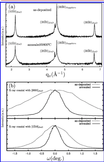
RESULTS AND DISCUSSIONThis work examines the structural characteristics of the ZnO layers by taking XRD measurements on the as-deposited and 800°C annealed samples. In addition to the intense sapphire (303̅0) Bragg reflection, only the ZnO (101̅0), (202̅0), and (303̅0) reflections are observed in the radial scans along surface normal of both samples (Figure 1(a)). The absence of other
diffraction peaks confirms that the ZnO films are of single crystallographic (101̅0) orientation, i.e., the m-plane orienta-tion. Upon annealing, the peak widths of all of the ZnO reflections significantly decrease. For instance, the full width at half-maximum (fwhm) of the ZnO (101̅0)ZnO reflection decreases from 9.38× 10⁻³to 5.36× 10⁻³Å−1, thus confirming the increase of the structural coherent length and the improvement of crystalline quality of the ZnO layers. Figure 1(b) shows the rocking curves of the (101̅0)ZnO specular reflection of the samples with the directions of incident X-rays along two orthogonal directions, either aligned or perpendicular to the ZnO c-axis. The dotted and solid curves are taken before and after thermal treatment, respectively. Along both directions, the peak widths significantly decrease after thermal annealing,
Figure 1.(a) XRD radial scans along the surface normal (θ-2θ scan) of an as-deposited ZnOfilm and a 800 °C annealed sample. The abscissa qzdenotes momentum transfer along the surface normal. (b) Theω rocking curves across the (101̅0)ZnOspecular reflection with impinging X-rays aligned with (top panel) ZnO c-axis and (bottom panel) [112̅0]ZnOa-axis, respectively.
revealing the decrease of the tilt angle of the ZnO layer. Moreover, the fwhm measured with an X-ray along the [0001]ZnO c-axis is always substantially larger than that along the [12̅10]ZnOa-axis, i.e. 2.489° vs 1.219° before annealing and
0.679° vs 0.464° after thermal annealing. This phenomenon reveals a higher structural perfection of the obtained m-plane ZnOfilm along the a-axis than that along the c-axis.
This work also examines the epitaxial relationship between the ZnO layer and the sapphire substrate by performing azimuthal cone scans (ϕ-scan) across the off-normal {101̅2}ZnO
and {033̅0}Al2O3reflections (Figure 2). In addition to revealing a
2-fold symmetry, all of the ϕ-scans indicate that the angular positions of {101̅ ± 2}ZnOreflections coincide with those of the
(033̅0)Al2O3 and (33̅00)Al2O3, which yield the in-plane relation-ship of [0001]ZnO||[12̅10]Al2O3 with an uncertainty of the polarity of the ZnO layer. Under this configuration, the lattice mismatches between ZnO and the underneath sapphire are 0.06% and 9.4% along ZnO a- and c-axes. A similar reduction is found in the fwhm of the {101̅2}ZnOpeaks from 1.39° to 0.68° upon annealing, manifesting the decrease of the twist angle. This decrease in both tilt and twist angles is often attributed to the reduction of both the edge and screw dislocation densities.13
Based on the angular positions of diffraction peaks, the interplanar spacings along three orthogonal axes are deduced, i.e., the surface normal m-axis and the two lateral directions, a-axis and c-a-axis. The as-deposited ZnO film has spacings of 5.630, 3.253, and 5.214 Å along the m-, a-, and c-axes, respectively. After thermal annealing, deviations of the interplanar spacings from the corresponding bulk values are all within 0.2% or less, indicating that the deposited layer is nearly strain free.
Figure 3(a) shows the cross sectional TEM images taken along the [1̅21̅0]ZnOzone axis of the 800°C annealed sample.
Figure 3(b) shows the corresponding SAED patterns. The coexistence of the rectangular and hexagonal lattices associated with ZnO and sapphire, respectively, confirms that the epitaxial relationship is (101̅0)⟨0001⟩ZnO||(101̅0)⟨1̅21̅0⟩Al2O3, which
agrees with the XRD data. Notably, the TEM image reveals several contrasting lines that propagate along the growth direction (marked by triangles). The lines are likely due to basal plane stacking faults (BSFs). This work further characterizes the nature of the contrasting lines by performing diffraction contrast analysis on the annealed sample. The contrasting lines are clearly visible in the dark field image recorded with diffraction vector g equal to (101̅0), as shown in Figure 3(c) but are out of contrast for g equal to (0002), as shown in Figure 3(d). According to the extinction rules, the stacking faults are out of contrast when g•R is equivalent to an integer. The displacement vectors R associated with three BSFs, I1, I2, and E,
are 1/6(22̅03), 1/3(11̅00), and 1/2(0001), respectively. The observed variation of g dependent contrast indicates that the BSFs in the m-plane ZnOfilm belong to intrinsic type I1and/
or I2. However, we cannot further distinguish between these
two types owing to insufficient information. Figure 4(a) shows the cross-sectional TEM image taken along the [0001]ZnOzone
axis, perpendicular to that of Figures 3, where no contrasting lines are identified. The associated SAED pattern in Figure 4(b) exhibits the hexagonal ZnO structure and sapphire diffraction patterns. Figures 4(c) and 4(d) show the darkfield images with gequal to (101̅0)ZnOand (1̅21̅0)ZnO, respectively. Again, these
images contain no contrasting lines. The absence of the contrast lines in this zone axis supports the assumption that the contrasting lines observed in Figure 3 originate from the BSFs, which lie on the planes perpendicular to this zone axis, thus ruling out the possibility of threading dislocations. These TEM images reveal that BSF is the dominant structural defect, and its density is estimated to be about 1× 106cm−1, which is quite
close to the value of the high quality m-plane ZnOfilms grown on the lattice-matched LaAlO3 substrate at a high growth
temperature by PLD.10
Based on the cross sectional TEM images, the thickness of the m-plane ZnOfilm is estimated to be ∼130 nm, which is also consistent with that derived from X-ray reflectivity measure-ment. According to the ALD growth mechanism,14each ALD cycle deposits one atomic layer of ZnO on the surface. Along the [101̅0]ZnO direction, each unit cell contains two atomic layers. Four hundred growth cycles deposit 200 unit cells and is anticipated to yield a total layer thickness of 200 × aZnO ×
(√3/2) = 112.6 nm. The measured thickness is significantly larger than that of theoretical calculations. In the case of ALD growth of c-plane ZnO, which consists of alternatively stacked Zn and O atomic layers, the experimental layer thickness correlates well with the anticipated value. However, each m-plane ZnO surface is composed of alternatively arranged Zn and O atomic rows. The steric effect, which functions well in the c-plane ZnO geometry, may not be as efficient in the current orientation, resulting in the growth of more than a monolayer in a reaction cycle. Detailed surface analysis is necessary to resolve this problem.
This work also examines the lattice matching across the interface by taking HR-TEM images near the ZnO/sapphire interface. Figure 5(a) shows the HR-TEM cross sectional image recorded with the [1̅21̅0]ZnOzone axis. Thefigure inset shows
the corresponding Fourierfiltered image using (1̅21̅0)Al2O3and (0002)ZnO reflections, where widely separated misfit disloca-tions, as represented by additional (1̅21̅0)Al2O3 half planes (marked by triangles) inserted into the sapphire lattice, scatter along the interface, owing to the 9.4% lattice mismatch across the interface. In contrast, Figure 5(b) shows the image taken
Figure 2. The azimuthal reflection scan across the {101̅2}ZnO and {303̅0}Al2O3planes. The in-plane relationship of the ZnOfilm and the sapphire substrate has been determined as {0002}ZnO||{112̅0}Al2O3and {0002}Al2O3||{112̅0}ZnO. The thermal annealing treatment improved the edge and screw dislocations of the as-deposited ZnOfilm as the fwhm decreasing from 1.39° to 0.68°.
along the [0002]ZnOzone axis, where regularly arranged atomic
rows are well resolved. Its Fourier filtered image formed by using (0006)Al2O3and (1̅21̅0)ZnOspots, as displayed in thefigure inset, reveals that four (1̅21̅0)ZnOplanes match three (0006)Al2O3 planes along the [1̅21̅0]ZnO direction; in addition each extra (1̅21̅0)ZnOplane corresponds to a misfit dislocation (marked by
triangles). The nearly evenly spaced misfit dislocations reveal the domain matching epitaxial (DME)15at the interface along [1̅21̅0]ZnO with an effective mismatch about 0.06%, which
agrees with the reported observation in samples grown by another method.5
Figures 6(a) and (b) show the surface morphology of the samples before and after annealing, as determined by atomic force microscopy (AFM), respectively. Surface morphologies of the nonpolar ZnOfilms grown by MOCVD and MBE methods usually exhibit striped features elongated along a direction either parallel or normal to the ZnO c-axis, depending on the growth conditions and terminated with specific crystal facets in some cases.6−8,11,14,16 In contrast, the granular features in Figure 6 confirm the absence of preferable lateral growth directions of the ZnO layer grown by ALD.7,8,11This difference can be attributed to the layer-by-layer growth nature and the self-limiting growth mechanism of ALD, for which the adatoms rather attach to surface lattice sites than congregate into clusters, resulting in atomically smoothly and fully covered layers. Moreover, both surfaces show only a slight amount of surface roughness. Upon annealing, surface feature size increases, accompanied by a decrease of the root-mean-square
(rms) roughness (as estimated from the square area of 1× 1 μm2) from 1.62 to 1.38 nm. Owing to the annealing induced
roughness degradation in c-plane ZnO grown on c-plane sapphire under similar growth conditions14and the (000± 1) polar surfaces having the highest surface energies, the improvement of surface roughness upon annealing in this work is owing to the low surface energy of the (101̅0)ZnO terminated surface.16
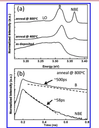
Moreover, this work investigates the optical properties of the m-plane ZnO and the influence of the annealing effect by taking time-integrated PL (TI-PL) measurements at 5 K (Figure 7(a)). A broad emission band appears in the spectrum of the as-deposited ZnO film at an energy below 3.31 eV. Upon annealing at 400°C, the emissions below ∼3.31 eV are strongly depressed; in addition, the broad emission band shrinks to a peak centered at ∼3.31 eV (marked as “B band”) with a line width of about 12 meV. Meanwhile, a peak centered at∼3.365 eV with a line width about 6 meV (marked as“NBE”) emerges. The absence of NBE emission and the presence of broad emission below 3.3 eV before annealing is likely due to residual organic functional groups, which are trapped inside thefilm and can be eliminated by annealing. The origin of the NBE band emission is mainly donor bound exciton (D0X) recombination
at a low temperature.17 The observed energy ∼3.365 eV is similar to that reported by Ku et al.12(3.364 eV) on the m-plane ZnO prepared by the same method but is higher than the commonly reported D0X transition ∼3.360 eV. The D0X resulted from the hydrogen and Al/Ga combination could have
Figure 3.The cross sectional TEM image (a) and the selected area electron diffraction (SAED) pattern (b) taken along the [1̅21̅0]ZnOzone axis. The darkfield images recorded with diffraction vector g equal to (101̅0)ZnOand (0002)ZnOare shown in (c) and (d), respectively. The contrast lines in the images marked by the triangles are identified to be the intrinsic type basal plane stacking faults.
the emission with similar energy but are unlikely the cause in this work because of the high temperature annealing treatment. In addition to impurity induced energy shift, the other possible cause of the D0X energy shift is the band gap deformation
induced by strain. In this work, the annealedfilm suffers a strain of∼0.2% tensilely along [101̅0]ZnO,∼0.3% compressively along the [0002]ZnO, and ∼0.05% tensilely along the [12̅10]ZnO.
Because of the complicated strain profile, it is difficult to predict the amount and direction of energy shift without sophisticated theoretical calculations. However, the band gap deformation
depending on the strain in the m-plane GaN thinfilm has been reported.18According to this report, the transition energies of the free excitons in the GaN would blue-shift for 6−8 meV due to the similar strain condition as reported in this work. Such a result suggests that the high D0X transition energy is attributed to the strain induced ZnO band gap deformation. Previous works have observed the B band at 3.31 eV in ZnOfilms and associated it with the basal plane stacking faults (BSFs).19−21 According to our structural analysis results, the m-plane ZnO films have a large density (∼106cm−1) of BSFs, i.e., significantly
Figure 4.The cross sectional TEM image (a) and the selected area electron diffraction (SAED) pattern (b) taken along the zone axis of [0001]ZnO. The darkfield images taken with diffraction vector g equal to (101̅0)ZnOand (1̅21̅0)ZnOare presented in (c) and (d), respectively.
Figure 5.The high resolution images of the interface with the zone axis of (a) [1̅21̅0]ZnOand (b) [0001]ZnO. The inset in (a) is the corresponding Fourierfiltered image using the (1̅21̅0)Al2O3and (0002)ZnOspots, and the Fourierfiltered image in (b) is formed by using the (0006)Al2O3and (1̅21̅0)ZnOreflections.
higher than that found in most c-plane ZnOfilms. Therefore, the B emission band is unsurprisingly the dominant feature in the low-temperature PL spectra of m-plane ZnO films. The small bump located at ∼72 meV lower than the B band, as marked by “LO”, is attributed to the longitudinal optical phonon (LO) replica of the B band. With thermal treatment at elevated temperatures, the intensity ratios of NBE to B band emissions increase from 0.16 to 0.19 and, then, to 0.76 for annealing temperatures of 400, 600, and 800 °C, respectively. The increasing intensity ratio implies that the thermal treatment with higher temperatures further eliminates the residual impurities and dislocations. Closely examining the TR-PL spectra of the 800°C annealed sample illustrated in Figure 7(b) reveals that the B band and NBE band decay curves exhibit a multiexponential decay, implying a complex transition mechanism. The decay curves can be wellfitted by using the
biexponential decay model to estimate the decay times. Based on thefitting results, the B band decay times are estimated to be∼500 ps and ∼40 ps with the ∼500 ps one dominating. The transitions of donor−acceptor pair (DAP) and two electron satellite (TES) were observed with energy∼3.31 eV at a low temperature.22,23The decay time of DAP at∼3.31 eV has been found in the range of 108−317 ps at a temperature of 77 K22as well as the decay time of TES found to be ∼27 ns at a temperature of 10 K.23However, to observe the TES transition band the ZnO material requires very high crystalline quality, and the emission intensity is much weaker than that of D0X; the
TES transition is thus the minor contribution to the 3.31 eV band in these samples. The longer lifetime of the B band emission implies the indirect transition resulting from the type-II quantum well formed by the BSF.21
For the NBE band in Figure 7(b), the decay times are approximate 58 and 175 ps; in addition, the 58 ps one is dominant. Under such a situation, the decay times of the dominating decay curves are taken as the major decay times. Many works have described the decay times of the D0X
transition in ZnOfilms and nanorods. For ZnO films, the decay times of∼100 ps at a temperature of 10 K were reported by Jen et al.24and Chichibu et al.,25while Liu et al.22reported 389 ps at 77 K. For ZnO in the form of nanorods, 432 ps was reported by Mohanta et al.26at a temperature of 4.3 K for those grown by MOCVD on the GaN substrate, and 32−80 ps was reported by Bekeny et al.27 at 10 K for those grown chemically in aqueous solution with different annealing processes. In this work, the NBE band decay time of about 58 ps is less than the D0X transition decay times mentioned above yet close to the
value of the ZnO nanorods grown in aqueous solution. This finding can be attributed to the large density of BSFs, which interfere with the D0X transition. Closely examining the TR-PL
spectra of the samples annealed at different temperatures (not shown here) reveals that the decay time of NBE band increases monotonically from 39, 53 to 58 ps with an elevated annealing temperature raised from 400, 600, to 800°C, respectively. The samples annealed at a higher temperature show a longer NBE decay time. Variations of the NBE to B band intensity ratio and the decay time as functions of annealing temperature indicate that the crystalline and optical properties of the as-deposited ZnOfilm are strongly and negatively influenced by the residual chemical function group. In addition to eliminating the residual chemical function group by low temperature annealing at 400 °C, thermal treatment repairs the defect and dislocations by a high annealing temperature, which is normally observed in crystalline bulk. However, thermal annealing is ineffective in eliminating the BSFs in the ZnOfilms.
■
CONCLUSIONSThis work demonstrates that ZnO thinfilms grown on m-plane sapphire by ALD are single crystallographic m-plane orientated. The epitaxial relationship between the m-plane ZnO film and the m-plane sapphire substrate follows (101̅0)⟨0001⟩ZnO|| (101̅0)⟨1̅21̅0⟩Al2O3 and reveals the DME with nearly perfect domain matching across the ZnO/sapphire interface along the [12̅10]ZnO direction. The smooth surface with isotropic
granular features confirms the layer-by-layer growth nature of ALD growth. Based on the PL spectra and the TEM images of the annealed samples, large density (∼106 cm−1) of intrinsic type BSF is identified as the major defect and may be the origin of the B band emission centered at about 3.31 eV in the PL
Figure 6.AFM images of the as-deposited (a) and annealed (b) m-ZnO films with surface roughness (Rrms) of 1.62 and 1.38 nm, respectively.
Figure 7.(a) The time integrated photoluminescence at 5 K of the as-deposited sample and sample annealed at 400 and 800°C. (b) The time-resolved photoluminescence at 5 K of the NBE and B band in the sample annealed at 800°C.
spectra. The time-resolved photoluminescence reveals that the NBE emission band is the D0X transition, and its decay time increases with the higher annealing temperatures. Our results further demonstrate that the ALD method is a highly promising alternative for fabricating high quality m-plane ZnO epi-layers on m-plane sapphires with a high surface flatness. Thermal annealing further improves the crystalline and optical qualities.
■
AUTHOR INFORMATIONCorresponding Author
*E-mail: [email protected] (C.-H.H.) and [email protected]. edu.tw (W.F.H.).
Notes
The authors declare no competingfinancial interest.
■
ACKNOWLEDGMENTSThe authors would like to thank the National Science Council of Taiwan for financially supporting this research under Contract No. NSC-99-2221-E-009-095-MY3, NSC-99-2112-M-006-017-MY3, and NSC-100-2112-M-213-002-MY3. Ted Knoy is appreciated for his editorial assistance.
■
REFERENCES(1) Lim, J. H.; Kang, C. K.; Kim, K. K.; Park, I. K.; Hwang, D. K.; Park, S. J. Adv. Mater. 2006, 18, 2720−2724.
(2) Jiao, S. J.; Zhang, Z. Z.; Lu, Y. M.; Shen, D. Z.; Yao, B.; Zhang, J. Y.; Li, B. H.; Zhao, D. X.; Fan, X. W.; Tang, Z. K. Appl. Phys. Lett. 2006, 88, 031911.
(3) Lee, J. W.; Kim, J. H.; Han, S. K.; Hong, S. K.; Lee, J. Y.; Hong, S. I.; Yao, T. J. Cryst. Growth 2010, 312, 238−244.
(4) Cagin, E.; Yang, J.; Wang, W.; Phillips, J. D.; Hong, S. K.; Lee, J. W.; Lee, J. Y. Appl. Phys. Lett. 2008, 92, 233505.
(5) Chauveau, J. M.; Vennéguès, P.; Laüegt, M.; Deparis, C.; Zuniga-Perez, J.; Morhain, C. J. Appl. Phys. 2008, 104, 073535.
(6) Kim, J. H.; Han, S. K.; Hong, S. I.; Hong, S. K.; Lee, J. W.; Lee, J. Y.; Song, J. H.; Park, J. S.; Yao, T. J. Vac. Sci. Technol., B: Microelectron. Nanometer Struct.–Process., Meas., Phenom. 2009, 27, 1625−1630.
(7) Moriyama, T.; Fujita, S. Jpn. J. Appl. Phys. 2005, 44, 7919−7921. (8) Chou, M. M. C.; Chang, L.; Chung, H. Y.; Huang, T. H.; Wu, J. J.; Chen, C. W. J. Cryst. Growth 2007, 308, 412−416.
(9) Ho, Y. T.; Wang, W. L.; Peng, C. Y.; Chen, W. C.; Liang, M. H.; Tian, J. S.; Chang, L. Thin Solid Films 2010, 518, 2988−2991.
(10) Wang, W. L.; Ho, Y. T.; Chiu, K. A.; Peng, C. Y.; Chang, L. J. Cryst. Growth 2010, 312, 1179−1182.
(11) Matsui, H; Tabata, H. J. Appl. Phys. 2006, 99, 124307. (12) Ku, C. S.; Lee, H. Y.; Huang, J. M.; Lin, C. M. Cryst. Growth Des. 2010, 10, 1460−1463.
(13) Liu, W.-R.; Hsieh, W. F.; Hsu, C.-H.; Liang, S. K.; Chien, F. S.-S. J. Appl. Crystallogr. 2007, 40, 924.
(14) Yang, S.; Lin, B. H.; Liu, W. R.; Lin, J. H.; Chang, C. S.; Hsu, C. H.; Hsieh, W. F. Cryst. Growth Des. 2009, 9, 5184−5189.
(15) Narayan, J.; Larson, B. C. J. Appl. Phys. 2003, 93, 278. (16) Zúñiga-Pérez, J.; Muñoz-Sanjosé, V.; Palacios-Lidón, E.; Colchero, J. Appl. Phys. Lett. 2006, 88, 261912.
(17) Hamby, D. W.; Lucca, D. A.; Klopfstein, M. J.; Cantwell, G. J. Appl. Phys. 2003, 93, 3214.
(18) Ghosh, S.; Waltereit, P.; Brandt, O.; Grahn, H. T.; Ploog, K. H. Phys. Rev. B 2002, 65, 075202.
(19) Schirra, M.; Schneider, R.; Reiser, A.; Prinz, G. M.; Feneberg, M.; Biskupek, J.; Kaiser, U.; Krill, C. E.; Thonke, K.; Sauer, R. Phys. Rev. B 2008, 77, 125215.
(20) Stampfl, C.; Van de Walle, C. G. Phys. Rev. B 1998, 57, R15052. (21) Yang, S.; Kuo, C. C.; Liu, W.-R.; Lin, B. H.; Hsu, H. C.; Hsu, C.-H.; Hsieh, W. F. Appl. Phys. Lett. 2012, 100, 101907.
(22) Liu, C. Y.; Zhang, B. P.; Binh, N. T.; Wakatsuki, K.; Segawa, Y. J. Cryst. Growth 2006, 290, 314.
(23) Mézy, A.; Anceau, S.; Bretagnon, T.; Lefebvre, P.; Taliercio, T.; Yi, G. C.; Yoo, J. Superlattices Microstruct. 2006, 39, 358.
(24) Jen, F. Y.; Lu, Y. C.; Chen, C. Y.; Wang, H. C.; Yang, C. C.; Zhang, B. P.; Segawa, Y. Appl. Phys. Lett. 2005, 87, 252117.
(25) Chichibu, S. F.; Onuma, T.; Kubota, M.; Uedono, A. J. Appl. Phys. 2006, 99, 093505.
(26) Mohanta, S. K.; Tripathy, S.; Zhang, X. H.; Kim, D. C.; Sho, C. B.; Yong, A. M.; Liu, W.; Cho, H. K. Appl. Phys. Lett. 2009, 94, 041901. (27) Bekeny, C.; Voss, T.; Hilker, B.; Gutowski, J.; Hauschild, R.; Kalt, H. J. Appl. Phys. 2007, 102, 044908.

![Figure 3. The cross sectional TEM image (a) and the selected area electron di ffraction (SAED) pattern (b) taken along the [1̅21̅0] ZnO zone axis](https://thumb-ap.123doks.com/thumbv2/9libinfo/7648465.139049/4.938.222.717.93.600/figure-sectional-image-selected-electron-ffraction-pattern-taken.webp)
![Figure 5. The high resolution images of the interface with the zone axis of (a) [1 ̅21̅0] ZnO and (b) [0001] ZnO](https://thumb-ap.123doks.com/thumbv2/9libinfo/7648465.139049/5.938.91.761.641.896/figure-high-resolution-images-interface-zone-axis-zno.webp)