IEEE TRANSACTIONS ON ELECTRON DEVICES, VOL. 42, NO. 6, JUNE 1995 1113
A
New Approach to Modeling the Substrate Current
of
Pre-Stressed and Post-Stressed
MOSFET’s
Jiuun-Jer Yang,
Steve
Shao-Shiun Chung, Member, IEEE, Peng-Cheng Chou, Chia-Hsiang Chen, and Mou-Shiung Lin, Member, IEEEAbstract-In this paper, we propose a closed form expression of a new and accurate analytical substrate current model for both pre-stressed and post-stressed MOSFET’s. It was derived based on the concept of effective electric field, which gives a more reasonable impact ionization rate in the lucky-electron model. This effective electric field, composed by two experimentally determined parameters, can be regarded as a result of nonlocal heating effects within devices. This model shows a significant improvement to the conventional local fieM model. One salient feature of the present model is that it allows us to characterize the time evolution of the substrate current of stressed MOSFET’s
for t h e j r s t time. Experimental verification for a wide variety of MOSFET’s with effective channel lengths down to 0.3 pm shows that the new model is very accurate and is feasible for any kind of MOS device with different drain structures. The present model can be applied to explore the hot carrier effect in designing submicrometer MOS devices with emphasis on the design optimization of a device drain engineering issue. In addition, the present model is well suited for device reliability analysis and circuit level simulations.
I. INTRODUCTION
T is well known that the substrate current
IB
can beI
used as a good monitor of the hot carrier effect [I]. Therefore, accurate prediction of the substrate current is crucial in designing reliable MOS devices and for analyzing circuit level reliability in VLSVULSI design [ 2 ] , [3]. In modeling the substrate current, the widely used form [4]-[6] for device analysis and circuit simulation utilizes the maximum electric field (E,) in the local electric field for the specific device structure as the dominant factor in hot carrier generation. This local field model for the substrate current agree reasonably well for large devices (e.g., L,tf>
1.0 pm). However, for the short channel MOS devices, the local field model fails to model the I B especially at high gate biases. To improve modeling accuracy, the impact ionization rate has to be modeled nonlocally by considering the two-dimensional (2- D) electric field effects as well as the heating effects [7], [8] (i.e., the solution by considering the nonisothermal effect).In addition to the drain current degradation in stressed devices, hot carrier induced oxide damages will in tum affect Manuscript received November 15, 1994; revised December 12, 1994. The review of this paper was arranged by Associate Editor K. Tada. This work was supported by the National Science Council, Taiwan, ROC, under Contract J.-J. Yang, S. S. Chung, and P.-C. Chou are with the Department of Electronic Engineering and Institute of Electronics, National Chiao Tung University, Hsinchu 300, Taiwan, ROC.
C.-H. Chen and M. S. Lin are with Taiwan Semiconductor Manufacturing Co., Hsinchu Industrial Park, Taiwan, ROC.
IEEE Log Number 9410965. NSC-8 1 -0404-EOO9-620.
the inner channel electric field distribution which then alter the substrate current characteristics [9]. Due to the difficulty in knowing the exact information about the amount and distribution of interface states or oxide charges, none has been made to model the substrate current characteristics of stressed MOSFET’s in analytical form. Undoubtedly, an accurate I B model for degraded devices is also essential for device and circuit level reliability studies.
To deal with the aforementioned problems, in this paper, we will propose a new analytical substrate current model based on the so-called effective electric field instead of the E, concept to calculate the impact ionization rate as well as the substrate current. Section I1 describes the new substrate current model and the new approach for modeling both the pre- stressed and post-stressed I B characteristics. Discussion and the comparison with reported models are also given. Section 111 presents a major application of this new model to study the hot carrier reliability of a new class of LATID (Large-Angle-
- Tilt implanted Drain) MOS devices. Conclusions are given in Section IV.
11. A NEW ANALYTICAL SUBSTRATE CURRENT MODEL In this section, a self-consistent analytical substrate current model for pre-stressed (fresh) and post-stressed MOSFET’s was derived by combining the concept of Lucky-Electron (LE) model and nonlocal field effect within devices. A series of LDD and LATID MOS [lo] devices with a wide range of process and device parameters, such as gate oxide thickness ('Tax), spacer width ( X , , ) , n- implantation dosage and im- plantation angle, are used to justify the accuracy of the present model. All the devices in this study have drawn channel width (W) 20 pm.
A. A New Substrate Current Model for MOSFET improved I B model can be expressed as
Based on the concept of the effective electric field, an
a
IB
=-ID
. ld . E,% . exp( -P/Eetf) (la)P
P
(Y
= - I D ’ (VDS - % h o t ) . exp(-P/Eeff). (1b) Here, the impact ionization rate ai = a.exp( -P/E,tf) is used, in which Eetf is used instead of E, in the conventional LE model. In the LE model, E, is expressed as (VDS - v D s a t ) / l d [4], where V D ~ ~ ~ is the saturation voltage. We define E,ff =
(VDS - VDhot)/ld as the effective electric field inside a device 0018-9383/95$04.00 0 1995 IEEE
I
1114
that is decisive for hot carrier behaviors. l d is regarded as
the effective hot carrier distribution length. (VDS - VDhot) is considered as the hot carrier driving force, in which VDhot is the hot carrier starting force. In developing this model, two-dimensional nonlocal field effect or the electron heating effect is included in the E,ff term which can be experimentally determined. To extract E e ~ , (lb) is rearranged to obtain another Eetf expression which gives
(2b)
-
P
-ID.O.(VDS-VDhot)
In
(
IB .PFor a given gate bias VGS and from the measured
1 ~ s - v ~ ~
and IB-VDS curves, two important parameters, VDhot and i d ,can be uniquely obtained by taking the following steps:
1) To calculate saturation voltages VDsat from
1 ~ s - v ~ ~
data, the method described in [l 11 was adopted here.In this method for determining VDSat, a function G is defined as
(3)
where gds = a I ~ s / a V D s is the conductance of the device. The first peak values of the G versus VDS curves correspond to the saturation point where VDS = VDsat- The VDsat value will be used as the initial guess for undetermined parameter VDhot
.
2) The surface impact ionization coefficients, a and ,B, adopt the values by Slotboom et al. [12] and are treated as fixed values in this model. With VDhot initially guessed as VD&, doing iteration between (2a) and (2b) using fixed point algorithm, VDhot and l d can be found.
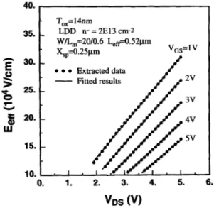
As (2a) implies, the relationship between E e ~ versus VDS exhibits a straight line. The intercept of the line with the VDS axis and the slope give VDhot and Zd values. For different gate voltages, Fig. 1 shows the linear rela- tionship between E e ~ and VDS for an LDD device, in which L, and
le^
represent the drawn channel length and effective channel length, respectively. VDhot and l d are found to beincreasing functions of VGS and can be expressed as an empirical form easily. The comparison of the IB character- istics given in Fig. 2 between the modeled and measured results for different channel length devices shows excellent agreements for wide range biases. Fig. 3 shows excellent agreements between modeled and experimentally measured IB characteristics for both LDD and LATID MO$ devices with wide range of gate oxide thickness, n- implantation dosage and angles. In particular, the effective channel length of the device in Fig. 3 (marked with solid triangle) with n- dosage 6E13 cmV2 and 45' implantation angle is 0.3 pm (extracted using the method described in [13]). One distinct feature of this new approach'is that VDhot and l d
are self-consistently extracted from experimental data so that very accurate modeled results can be achieved. Moreover, no additional fitting procedure is needed.
lEEE TRANSACTIONS ON ELECTRON DEVICES, VOL. 42, NO. 6, JUNE 1995
n
E
s
d 0 F v5
w
40-I
35. 30. 25. 20. 15. 10.-
To,=14nm LDD n- = 2E13 cm-2 WiLm=20/0.6 Le&.52pm XSp=0.25pm V,,=lV-
Extracteddata Fitted results 2 v 3 v 4 v - _. 0 . 1 . 2 . 3 . 4 . 5 . 6 . VDS(v)
The extracted effective electric field versus the drain voltages of an Fig. 1.
LDD device.
.-
~0 . 1 . 2 . 3 . 4 . 5 . 6 .
Fig. 2. Comparison of the substrate current between measured and modeled results for two different channel length LDD devices. Dash lines are the results of (4b). Cross marks are the results of the new 1~ model. The device parameters are To, = 140 A, n- dose = 2E13 cm-' and Xsp = 0.25 pm.
B. Substrate Current Characteristics for Degraded MOSFET's Owing to the existence of oxide trapped charges and inter- face states after hot carrier injection, the electric field in the surface depletion area changes. As a result, the E e ~ varies and then modulates the magnitude of the substrate current. Through the charactization of the time evolution of VDhot and l d , the substrate current of post-stressed MOSFET can be adequately modeled. To examine the effects of different types of trapped charges and interface states on the variations of VDhot and l d in n-channel devices, we designed a two-step dc hot carrier
YANG et al.: A NEW APPROACH M MODELING THE SUBSTRATE CURRENT OF MOSFET'S 1115 n
a
U m I 1oo
1 0" lo-* 1 0" 1o4
1 0" 1o6
1 0-' 1 0" 1o9
i doOT,,=SMI. n-=4E13, LDD, L&.45pn ATox=lOnm, n.=4E13, LDD, L&.51pm WTOx=14nm, n.dE13, LDD, L&.44pm OTOx=8nm n'=4E13,45" LATID, Le@.36pm
I
AT0=8nm, n-=6E13,45" LATID, Le@.3pnFig. 3. Comparison of the substrate current between measured and modeled results for LDD and LATID MOS devices with wide range of gate oxide thickness, n- implantation dosage and angle. Symbols are measured data. Solid lines are modeled results. The L , and X , , of all devices are 0 . 6 pm and 0.15 pm, respectively. 45' LATID means the n- implantation angle is 45' (as illustrated in Fig. 7).
stress on devices. The device was first biased at VGS = 1 V and VDS = 7 V for lo4 seconds stress, then, subsequently biased at
VGS = VDS = 7 V for another lo4 seconds stress. The device characteristics were measured during certain period of the stress time. A fixed base level charge pumping measurement
[14] was also performed to identify the types of the oxide damages after carrier injection.
I) Eeff Variation During Hot Hole Injection: Divices stressed at VGS = 1 V and VDS = 7 V will cause hole injection, since the direction of the momentum of holes is toward the gate while electron is to the drain. The hole injection generates hole traps in the oxide as identified by charge pumping method, similar measurement results were also ob- served and well explained in [9]. The time evolution of parameters VDhot and l d for a LDD device during hot hole
injection are shown in Fig. 4. VDhot values vary slightly,
while the l d values increase with stress time and the l d -
V i s curve shift in parallel, the resultant E e ~ decreases. In other words, hole traps reduce the
IB
current. Using the extracted parameter values, the modeled I B characteristics of a post-stressed device and the comparison with experiment for two successive stress time are given in Fig. 5 which shows excellent agreement. The new model successfully characterizes the E e ~ variations.2 ) Eeff Variation During Hot Electron Injection: The same device was continuously biased at VGS =
VDS
= 7 V for additional stress to generate hot electron injection. Judging from charge pumping measurement, the latter electron injec- tion generates large amount of negative charges, which can be negative oxide traps and acceptor-type interface states as explained in [9]. The time evolution of VDhot and l d during hotelectron injection was evaluated and a similar result to Fig. 4 was obtained. The Zd-VGS curve shifts parallelly, however, the
2.0 n 1.8 1.6 l?
5
1.4 1.2 1 .o 2.0 1.5 U-
n5
'd 1.0 c>"
0.5 0.0t
I WL,=20/0.6 Leff=O.52pm LDD ~ = 2 E 1 3 c m - ~ -.- 0 . 1 . 2 . 3 . 4 . 5 . 6 .Fig. 4. Time evolution of VDhot and Id during hot hole injection at VGS = 1 V and VDS = 7 V for the same device in Fig. 1. The Id curve shifts upward.
n
a
U m I 10 10 10 10 -9 -10Y'
3v
I V 0 . 1 . 2 . 3 . 4 . 5 . 6 . VGS(v)
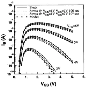
Fig. 5. Comparison of the post-stressed substrate current between measured and modeled results for the same device as in Fig. 1. The lines are the measured data for fresh, after 100 sec stress and after lo4 sec stress, respectively. Cross marks are the modeled results.
Id values decrease with stress time in contrast to the effect of
aforementioned hole injection. The VDhot-VGS curve merely increasingly shifts to a relatively large value (0.03 V in this case) in a very short time (less than 50 seconds) stress and then almost unchanges in the following stress, the resultant
E e ~ increases with stress time. In other words, negative oxide
traps and acceptor-type interface states enlarge
IB.
3) The E e ~ Variation of Post-Stressed MOSFET's in Reverse Mode Operation: The reverse mode I B characteristics (ex- changing source and drain electrodes) were also characterized to study the influence of source side oxide damages on the
1116
hot carrier behaviors. The stress was done at Vis = 1 V and VDS = 7
v
for io4 seconds. The parameters vDhot and ldshow very different variations with stress time and VGS as compared with the aforementioned two forward mode cases. VDhot values increase especially at higher VGS biases. On the contrary, l d values decrease gradually with increasing VGS.
Higher gate bias magnifies the oxide damage effect at the source side. Longer stress time has larger variations. The resultant effect of the source side oxide damages reduce E,R, and thereby giving rise to the decrease of I B with stress time. The reverse mode E e ~ of LDD devices has larger degradation than that of LATID devices which will be explained later.
C. Discussion
Several implications from the comparison of the present model with the conventional ones [4]-[6] can be drawn as follows:
In modeling the substrate current of a conventional single drain MOS device, the following form of the con- ventional approach [5] based on the local field concept is widely used
a
IB
=-ID
.
l d.
E, * exp( -@/E,) ( 4 4P
P
. e x P ( - @ l d / ( V D S - VDsat)), (4b)
(Y
= - I D
.
(VIS - VDsat)in which E, = (vDS-vD,,t)/ld is generally considered as the maximum electric field along the channel. Two approaches are commonly used to calculate E,. (a) VD,,, is extracted experimentally by utilizing the idea implied in (4b) as first described in [5], and the l d is
presumably formulated related to the device geometry [15] which is treated as the characteristic length that is bias independent. In this appraoch to model I,, (Y
and
P
values can be extracted experimentally from (4b) as long as VDsat and Id have been calculated. (b) The E, value and its expressions are obtained or fitted from device simulation or analytical electric field models [41,[6]. The modeled results of (4b) using approach (a) are
compared with the new model and the measured data as shown in Fig. 2. Since the model parameters are not all directly extracted from experimental data self- consistently, the above approaches more or less require adjustable parameters (e.g., (Y and
P)
to reasonablymatch their models with measured data. However, their results often mismatch the I B values at higher VGS values since their E, expressions fail to reflect the complicated electric field variations over wide biases. In the new approach here, E e ~ really reflects the 2-D electric field effect so that the overall impact ionization rate (Y
.
exp(-P/E,R) accurately determines theIB
value.
One salient feature of the new approach is that it can be applied to any kind of MOS devices with different drain structures (e.g., LDD, LATID devices). However, the conventional approaches to obtained
E,
were derived[EEE TRANSACTIONS ON ELECTRON DEVICES, VOL. 42, NO. 6 , JUNE 1995 based on the conventional single drain MOS devices only, and needs individual modification for different LDD structures.
The extracted VDhot is smaller than its initial guess VDsat. For the first time, this model suggests that the hot carrier driving force should be ( VDS - VDhot) instead of
widely used value (VDS
-
V D ~ ~ ~ ) which reflects only maximum electric field. In other words, the E, concept is not adequate to present 2-D effect inside devices. Fig. 6 compares the positions of VDsat and VDhot on the IDS-VDS curves of a LDD device. This implies that the drain biased at a point below saturation region has already significantly contributed to the impact ionization. Moreover, the effective hot carrier distribution length is an increasing function of VGS and is independent of the drain bias. For circuit simulation use, VDhot and Id canbe well formulated as VDhot = VDO
+
VDI.
VGS+
V D ~.
V& and l d = ld~+ld~.V&+ld:!.V&, respectively. From the newIB
model and the extracted E e ~ , the carrier energy distribution inside a device can be figured out as follows. (a) For a given VDS, a higher VGS bias results in a smaller hot carrier driving force (V& - VDhot) and longer effective distribution length, reflecting the profile that the carrier energy in such biases has a more slower variation and wider distributions. (b) For a given VGS, larger VDS results in a higher ( VDS - VDhot) value across the same distribution length so that gives a higher peak electric field.Various stress experiments performed at different biases and devices show that the hot carrier induced oxide damages have minor effect on the overall apparent hot carrier driving force (VDS - VDhot). However, Id
is sensitive to the net amount of total trapped oxide charges. The parallel shift of ld curves in Fig. 4 can be
characterized and empirically formulated as a function of time given by
A l d = 3.0712 X . lo&) (cm). ( 5 ) With VDhot approximately unchanged, the stressed 1~
characteristics (Fig. 5 ) can be predicted by employing ( 5 ) with very high accuracy.
During the hot carrier injection, large amount of inter- face states are generated below the sidewall spacer at the drain side which then in reverse mode operation electrically deplete mobile carriers at the source side and thus induce additional series resistance there. The variations of (Vis
-
VDhot) and i d in reverse modeare caused by an extra voltage drop at the source side due to the increased series resistance which effectively decreases drain bias and gate bias. This resistance ef- fect is more obvious at higher VGS biases, since the larger drain current enhances more larger voltage drop across the damaged region. Assume AV(V&) is the voltage dropped at source region, the effective gate bias excluding resistance effect reduces to (VGS-AV(VGS)), which reduces the drain current. Owing to less amount of conducting carriers in the channel, the carriers in the
YANG ef al.: A NEW APPROACH TO MODELING THE SUBSTRATE CURRENT OF MOSFET'S 1117 T0,=14nm LDD n-=2E13 cm-2
I
w&=20/0.6 Le~0.52pm XS,=0.25pm na
E
v 10. 8. 6. 4. 2. n - -..
0 . 1 . 2 . 3 . 4 . 5 . 6 . vDS(v)
Fig. 6.same device in Fig. 1.
Comparison of V D and ~ VDhot ~ ~ on the 1 ~ s - v ~ ~ curves for the drain side are easily to be depleted by the lateral electric field, the device thus exhibits a smaller Id value. The
effective drain bias excluding resistance effect is also reduced to (VDS - AV(V&,)). The hot carrier driving force across the impact ionization region becomes
where b h o t = (VDhot,O
+
Av(vGS)) and VDhot,O is the hot carrier starting voltage without oxide damages at source side. Because the drain bias applied at drain electrode is still VDS, the characterized resistance effect is emerged into VDhot, which makes the overall VDhot values larger at higher Vis. In summary, the influence of source side oxide damages on theIB
characteristics comes from the lowering of the hot carrier driving force and the narrowing of the effective distribution length. The degree of the variations of VDhot is larger than that of l d , the resultant Eeff within devices is reduced. Thedegradation of LDD devices is larger than LATID devices since LDD devices suffer greater hot carrier effect (see Fig. 8). Large amount of interface states are generated which mostly located outside the gate edge [lo], [ 161 in LDD device. Therefore, the resistance effect of LDD devices is more significant.
111. HOT CARRIER ANALYSIS OF VARIOUS LDD-STRUCTURE DEVICES USING Eeff
By applying the present
IB
model to a set of n-channel LATID MOS devices [IO] and evaluating the performance degradation of these devices under hot carrier effect, we will demonstrate that E e ~ can be also used as a good monitor of the hot carrier reliability. The LATID MOS device samples were fabricated using the standard poly-silicon gate CMOS technology. The gate oxide is 140A.
After the conventionalgate etching step of CMOS process, a phosphorus n- tilt angle implantation of dosage 2E13 c n r 2 with energy 80 kev was performed with tilt angle 0 (0' to 60') from the source and
drain sides by rotating the wafer automatically. Then heavy Arsenic n+ implant was done by a 0.25 pm vapor-deposited oxide spacer width offset from the gate edge for all devices. The drawn channel length of all devices discussed here is 0.6 Pm-
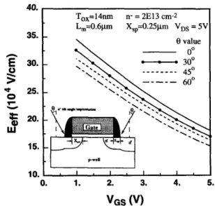
The extracted effective electric fields of LATID MOS de- vices with various tilt angles are compared in Fig. 7. Smaller effective electric field is observed for devices with larger implantation angle although their drain current is larger as presented in our reported results [ 171. Due to gate control over the longer n- region and the separation of main current path away from maximum heating points within device formed by large tilt angle implantation, the resultant E e ~ in LATID MOS device is thus reduced. To examine the relationship between
Eeff and hot carrier reliability, we performed a dc hot carrier
stress biased at VGS = 3.5 V and VDS = 7 V to evaluate their interface state generation and the associated normalized drain current degradation ( A I D / I D o ) . The results are given in Fig. 8. The interface states (AN;,) are characterized by charge pumping measurement. We found that LATID device with larger implantation angle has smaller amount of AN;, and less A I D / I D o , which means that hot carrier effect in such device is alleviated. The trend of the hot carrier effect in the characterized devices is consistent with that given by extracted E e ~ . In other words, device with smaller E e ~ will suffer less hot carrier effect and vice versa. E e ~ successfully quantitizes hot carrier effect. Therefore, to compare the hot carrier reliability between various devices, in particular for the device drain engineering applications, E e ~ and its components (VDS - VDhot, and I d ) can provide more detailed physical information of the hot carrier effect than the conventional measured I B / I D ratio that people commonly used.
IV. CONCLUSION
In this paper, a new concept for modeling the hot carrier induced MOS device substrate current is proposed. Three major improvements over the previous models are 1) an effective electric field is introduced in the model to account for the hot carrier heating and 2-D field (nonlocal) effects within devices; 2) the new analytical substrate current model is rather flexible and suitable for any kind of MOS devices with different drain structures; and 3) it enables us to model thepost- stressed I B characteristics for the first time. This study also finds that different types of oxide damages show very different influences on the effective electric field. The post-stressed
IB
characteristics are skillfully modeled through characterizing the time evolution of effective electric field. The new approach accurately calculates the I B characteristics for MOS devices with effective channel length down to 0.3 pm.
One major application of the present model is to explore the hot carrier effect in designing a submicron MOS device with emphasis on the drain engineering issue. With a trade- off between the use of n- implantation dosage and angle, we conclude that the design optimization of a hot carrier
1118 IEEE TRANSACTIONS ON ELECTRON DEVICES, VOL. 42, NO. 6 , JUNE 1995 n
E
d 0 F U5
w
To,=14nm n- = 2E13 cm-2 Lm==0.6pm Xsp=0.25pm VDs = 5\ 35.-
30.-
-
30’ 25.-
20.-
15.-
0. 1. 2. 3. 4. 5. VGS(v)
Fig. 7. Extracted effective electric field for LATID MOS devices with various n- implantation angles. The insert is a schematic diagram of a LATID MOS device.
ld2
ToX=14nm, n-=2E13~m-~, Lm=0.6pm Stress @VDs=lV, V,s=3.5V
AI&,, evaluated @ V & l . lV, VGS=5V
n Y
E
0 U c 2- U - A A+ +
xx
-
d
I
e
%
U 0 1 0’ 102Id
1$ la5Time (sec)
Fig. 8. Time evolution of hot carrier generated AN,, and linear region drain current degradation for LATID MOS devices with various implantation angles.
resistant LATID device can be better understood through the use of the newly developed substrate current model. The newly developed substrate current model can be. further incorporated into SPICE models to evaluate the circuit level hot carrier reliability [ 181.
REFERENCES
[ l ] E. Takada and N. Suzuki, “An empirical model for device degradation due to hot-carrier injection,” IEEE Electron Device Lett., vol. EDL-4, [2] Y. Leblebici and S.-M. Kang, “Modeling of nMOS transistors for simulation of hot-carrier-induced device and circuit degradation,” IEEE Trans. Computer-Aided Design, vol. 11, no. 2, pp. 235-246, 1992. pp. 111-113, 1983.
[31
191
S. S. Chung, P.-C. Hsu, and J.-S. Lee, “A new MOSFET hot carrier model in SPICE feasible for VLSI reliability analysis,” in Proc. Int’l VLSI Technology, Sys., and Appl., Taipei, Taiwan, May 22-24, 1991, pp. 283-287.
P. K. KO, “Hot-electron effects in MOSFET’s,” Ph.D. Dissertation, Dept. of Electrical Engineering and Computer Science, Univ. of California, Berkeley, June 1982.
T. Y. Chan, P. K. KO, and C. Hu, “A simple method to characterize substrate current in MOSFET’s,” IEEE Electron Device Let?. , vol. EDL-
G . 4 . Huang and C.-Y. Wu, “An analytical saturation model for drain and substrate currents of conventional and LDD MOSFET’s,” IEEE Trans. Electron Devices, vol. 37, no. 7, pp. 1667-1677, 1990. C. G. Hwang and R. W. Dutton, “Substrate current model for submi- crometer MOSFET’s based on mean free path analysis,” IEEE Trans. Electron Devices, vol. 36, no. 7, pp. 1348-1354, 1989.
S. S. Chung and G.-H. Lee, “Accurate modeling of the energy-dependent hot electron effects in submicron MOSFET’s,” in Proc. 1993 Int. Confi Solid State Devices and Materials, Chiba, Japan, Aug. 28-Sept. 1, 1993, pp. 479-481.
P. Heremans, R. Bellens, G. Groeseneken, and H. E. Maes, “Consistent model for the hot-carrier degradation in n-channel and p-channel MOS- FET’s,” IEEE Trans. Electron Devices, vol. 35, no. 12, pp. 2194-2209, 1988.
T. Hori, J. Hirase, Y. Odake and T. Yashi, “Deep-submicrometer large- angle-tilt implanted drain (LATID) technology,” IEEE Trans. Electron Devices, vol. 39, no. 10, pp. 2312-2324, 1992.
W. Y. Jang, C. Y. Wu, and H. J. Wu, “A new experimental method to determine the saturation voltage of a small-geometry MOSFET,” Solid-state Electron., vol. 31, pp. 1421-1431, 1988.
J. W. Slotboom, G. Streutker, G. J. T. Davids, and P. B. Hartog, “Surface impact ionization in silicon devices,” in IDEM Tech. Dig., pp. 494497, 1987.
S. S. Chung and J.-S. Lee, “A new approach to determine the drain- to-source series resistance of LDD MOSFET’s,” IEEE Trans. Electron Devices, vol. 40, no. 9, pp. 1709-1711, 1993.
S. S. Chung, J.-J. Yang, C.-H. Tang, and P.-C. Chou, “Characterization of hot electron induced interface states in LATID MOS devices using an improved charge pumping method,” in Proc. 1993 Int. Con$ Solid State Devices and Materials, Chiba, Japan, Aug. 28Sept. 1, 1993, pp. 84 1-843.
T. Y. Chan, P. K. KO, and C. Hu, “Dependence of channel electric field on device scaling,” IEEE Electron Device Lett., vol. EDL-6, no. IO, pp. 551-553, 1985.
F.-C. Hsu and H. R. Grinolds, “Structure-enhanced MOSFET degra- dation due to hot-electron injection,” IEEE Elecfron Device Letr., vol. J.-J. Yang, S. S. Chung, P.-C. Chou, C.-S. Chen, and M.-S. Lin, “Suppression of the hot carrier effect in designing LATID MOS devices based on a new substrate current model,” in Proc. Int’l VLSI Technology,
Sys., and Appl., Taipei, Taiwan, May 12-14, 1993, pp. 173-177. J.-J. Yang, S. S. Chung, P.-C. Chou, C.-S. Chen, and M.-S. Lin, “A consistent drain and substrate current model of LDD MOS devices for circuit simulation,” in Proc. Int’l Workshop on VLSI Process and Devices Modeling (VPAD), Nara, Japan, May 14-15, 1993, pp. 140-141. 5, pp. 505-507, 1984.
EDL-5, pp. 71-74, 1984.
Jiuun-Jer Yang was born in Kinmen, Fukien, ROC, in 1967. He received the B.S. degree in electrical engineering from National Cheng-Kung University, Taiwan, in 1989, and the M.S. degree in electronic engineering from National Chiao-Tung University, Taiwan, in 1991. He is currently working toward the Ph.D. degree in the Institute of Electronics, Na- tional Chiao-Tung University. His current research interests include VLSIAJLSI technology, device de- sign, device modeling and simulation, and reliability study of miniaturized MOS devices.
YANG ef al.: A NEW APPROACH TO MODELING THE SUBSTRATE CURRENT OF MOSFET’S 1119 Steve Shao-Shiun Chung (S’83-M’85) received
the B.S. degree from the National Cheng-Kung University, Taiwan, in 1973, the M.Sc. degree from the National Taiwan University in 1975, and the Ph.D. degree from the University of Illinois at Urbana-Champaign, in 1985, all in electrical engi- neering.
From 1976 to 1978, he worked for an electronic instrument company as Head of the R&D division and subsequently as Manager of the Engineering Division. From 1978 to 1983, he was with the Department of Electronic Engineering and Technology at the National Taiwan Institute of Technology (NTIT) as a Lecturer. He was also in charge of an Instrument Calibration Center at NTIT. From 1983 to 1985, he held a research assistantship in the Solid State Electronics Laboratory and the Department of Electrical and Computer Engineering at the University of Illinois. In September 1985, he served at NTlT again as an Associate Professor in the Department of Electronic Engineering. Since August 1987, he has been with the Department of Electronic Engineering and Institute of Electronics, National Chiao Tung University, and has been a Full Professor since the Fall of 1989. His current teaching and research interests are in the areas of solid- state device physics and VLSI technology; Spice device modeling; numerical simulation and modeling of submicrometer and deep-submicrometer MOS devices, SO1 devices, nonvolatile memories, and m ’ s ; charactenzation and reliability study of VLSI devices and circuits; and computational algorithms for VLSI circuits. He has authored and co-authored more than 60 international journal and conference papers in the above areas.
Dr. Chung has served as a Technical Program Committee Member of the ASIC Conference, IEEE, since 1989.
Peng-Cheng Chou was born in Taiwan, ROC, in 1968. He received the B.S. degree in electrical engineering from National Cheng-Kung University, Taiwan, in 1991, and the M.S. degree in electronic engineering from National Chiao-Tung University, Taiwan, in 1993. His thesis study is on the design of a submicrometer large tilt-angle implanted drain MOS device and process. His research interests are in the area of VLSIAJLSI technology, device design and reliability study of deep-submicrometer MOS devices.
Chia-Hsiang Chen received the B.S. degree in electrophysics and M.S. degree in electro-optics from the National Chiao-Tung University, Taiwan, in 1981 and 1985, respectively.
In 1985, he worked on the GaAs MESFET pro- cessing at MRLIITRI. During 1986-1989, he was involved in the processing of infrared detector based on both the InSb CID arrays and HgCdTe PV, PC arrays in CSIST Taiwan. In 1989, he joined R&D department of TSMC and from then he has worked on the process development and device design. Now he is the manager of device engineering section, Technology Development Division, Taiwan Semiconductor Manufacturing Company, Ltd., Hsin-Chu, Taiwan.
Mou-Shiung Lin (M’82) received the B.S. degree in physics from the National Taiwan University, Taiwan, in 1975, and the M.S. and Ph.D. degrees in applied physics from Harvard University, Cam- bridge, MA, in 1978 and 1982, respectively. He was a visiting scientist at the Massachusetts Institute of Technology while working on this Ph.D. disserta- tion.
From 1982 to 1984, he worked at IBM Corp., Essex Junction, VT, where he was involved in the develooment of lJ3M first two eenerations of CMOS technologies, CMOS I and CMOS 11. He joined AT&’fBell Laboratories at Murray Hill, NJ, in 1984. At Bell Labs., he spent five years working on the advanced VLSI packaging (AVP) technology for multichip interconnection based on the silicon substrate and flip-chip solder joint approaches. He defined and shaped the AVP technology. He then spent a year working on semiconductor lasers and optical amplifiers for use in optical communication systems. He joined Taiwan Semiconductor Manufacturing Company (TSMC), Taiwan in 1990, and is now the director of the R&D Division. He has been leading the R&D teams to accomplish the development of the 0.8 um, 0.6 um, 0.5 um technologies; with applications in logic, ASIC, mixed-mode, 1M high speed SRAh4, 4M DRAM, 4M EPROM, 1M flash, EEPROM PLD, 8M mask ROM. The teams are now working on the 0.35 p m technology development, and some exploratory module development on the 0.25 p m and below technologies. He has been an Adjunct Professor at the National Taiwan University in 199&1991 and National Chiao-Tung University in 1991-1993. He authored or co-authored over 50 joumal or conference papers in the areas of semiconductor devices. VLSI technologies, VLSI packaging, and semiconductor lasers.
Dr. Lin is listed in Marquis’ Who’s Who in Frontiers of Science and