Low Voltage and High Speed SONOS Flash Memory
Technology: The Strategies and the Reliabilities
Steve S. Chung
Department of Electronics Engineering, National Chiao Tung University, Taiwan
TEL: 886-3-5731830 Fax: 886-3-5734608 email: schung@cc.nctu.edu.tw The flash memory has been evolved from floating gate to the nitride-trapping storage type-SONOS, and even progresses toward the nano-crystal memory in the future. Among them, floating gate flash memory has been one of the most successful nonvolatile memories for the largest volume production, in the past two decades. In comparison, SONOS-type trapping storage has reliability issue and has yet not been fully approved for mass production. On the other hand, the floating gate flash memory requires high control gate voltage for programming which limits the device scaling and reliability, while the SONOS type flash needs to overcome the reliability issues, especially the tunnel oxide and data retention. In this paper, we address different strategies for designing SONOS-type flash memories with low voltage operation, for achieving good reliability while keeping high speed performance. Various schemes will be demonstrated to meet the low voltage and high speed requirements. Also, the strategies for achieving excellent data retention will be specifically presented.
Introduction
In the past two decades, floating gate memory has been the mainstream of flash memory products such as memory stick, smart card, mobile applications etc. [1] However, the requirements of high voltage operation and/or its compatibility with the logic process have been the roadblocks for developing low power and low cost applications. As a consequence, SONOS type flash memory has been involved as a potential candidate to replace the floating gate technology. However, the use of SONOS cell as a commercial product has not yet been so popular comparing to the floating gate cells. It lies in the fact that the charge loss in a SONOS cell can not be well-controlled as a result of the inherent nature of the ONO structure with very thin tunnel oxide for the programming and erase.
In general, in a SONOS cell, the program/erase operation is achieved via the tunneling of electrons/holes through the very thin tunnel oxide. As a result, the cell has poor retention due to this thin tunnel oxide. In order to improve the retention of the SONOS cells, a relatively thick bottom oxide is used to prevent charge loss such as NROM cell [2] or by the using of high-k ONO layer [3-4]. However, the thicker bottom oxide increases the difficulty for low voltage and/or low power design.
In this paper, the strategies for achieving high performance design of a SONOS type flash memory while keeping excellent reliability will be introduced. The fundamental concepts toward a low voltage operating scheme will be addressed.
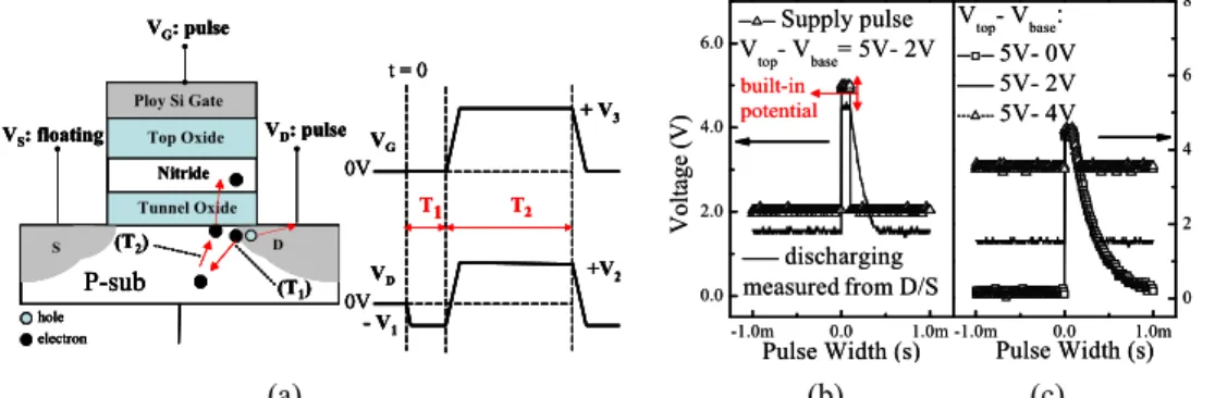
VG: pulse P-sub Ploy Si Gate S D Top Oxide Nitride Tunnel Oxide electron hole (T1) VD: pulse VS: floating (T2) VG: pulse P-sub Ploy Si Gate S D Top Oxide Nitride Tunnel Oxide electron hole (T1) VD: pulse VS: floating (T2) 0V + V3 +V2 t = 0 T1 T2 0V - V1 VG VD 0V + V3 +V2 t = 0 T1 T2 0V - V1 VG VD VG: pulse P-sub Ploy Si Gate S D Top Oxide Nitride Tunnel Oxide electron hole (T1) VD: pulse VS: floating (T2) VG: pulse P-sub Ploy Si Gate S D Top Oxide Nitride Tunnel Oxide electron hole (T1) VD: pulse VS: floating (T2) 0V + V3 +V2 t = 0 T1 T2 0V - V1 VG VD 0V + V3 +V2 t = 0 T1 T2 0V - V1 VG VD
The Experimental Memory Cells
The n-channel flash SONOS cells with ONO layer thickness (50/40/50) (Ao), W/L= 0.2/0.2(Pm), were fabricated using 0.13Pm CMOS technology. Medium-doped n+
-region in the S/D extension was used to maintain a high breakdown voltage.
Design of Low Voltage Operating Schemes
In the past several years, three strategies are commonly used to design reliable SONOS flash memory cells. One is based on the ONO layer band-gap engineering approach [5-6]. The second one is using high-k in the ONO layer [3-4], and the last one is using low voltage operation schemes. With a controlled band structure in the ONO layer, the charge storage in the nitride layer will see a deeper energy level such that charge loss can be reduced. By using the high-k as oxide replacement in the ONO layer gives rise to a reduction of the leakage current as well as the charge loss. However, to cope with the need, operation scheme is the most straightforward one. In a series of study proposed by us in [7-8] using operating scheme approach is one of the feasible solutions with low voltage, high speed, and excellent data retention capability. Not only the operating voltage can be reduced to below 5V, very high speed can also be achieved. The design of reliable SONOS with operating scheme approach will be highlighted as the following. Injection Scheme for Holes- BBHHI
Fig. 1(a) shows the schematic for hole injection scheme, called back-bias assisted hot hole injection (BB-HHI). During T1, source and drain are kept floating with a positive
bias (+Vtop) applied at the bulk, where source or drain-substrate junction capacitance is
charged [3]. At the end of T2, bulk bias is turned-off (the junction is switched to reverse
bias mode) and changed to +Vbase, the generated holes in the space charge region are then
injected into the nitride storage through discharging, during the VB falling pulse edge, T3,
as can be seen from Figs. 1(b) and 1(c).
(a) (b) (c)
Fig. 1 (a) Experimental set up and timing diagram for BB-HHI injection. (b) The supplying pulse(square) and the discharging waveform at S/D for the case of Vtop- Vbase= 5V- 2V. (c) The discharging condition for three different Vtop- Vbase cases.
Fig. 2(a) shows the 'VT versus the pulse height, in which a higher level Vtop gives a
larger'VT. Moreover, it also shows the 'VT as a function of 'VB (=Vtop- Vbase), and the
'VT reaches its maximum at 'VT = 4V. For example, comparing the conditions of Vtop
-Vbase =7V- 2V and Vtop- Vbase =7V- 0V, although the condition of Vtop- Vbase =7V- 0V has
larger space charge region variation during the transition from forward bias mode to reverse bias mode and the hot holes generated via discharging induced breakdown are
-1.0m 0.0 1.0m 0.0 2.0 4.0 6.0 discharging measured from D/S Supply pulse Vtop- Vbase= 5V- 2V Vo lt ag e ( V ) Pulse Width (s) -1.0m 0.0 1.0m 0 2 4 6 8 V top- Vbase: 5V- 0V 5V- 2V 5V- 4V Pulse Width (s) built-in potential -1.0m 0.0 1.0m 0.0 2.0 4.0 6.0 discharging measured from D/S Supply pulse Vtop- Vbase= 5V- 2V Vo lt ag e ( V ) Pulse Width (s) -1.0m 0.0 1.0m 0 2 4 6 8 V top- Vbase: 5V- 0V 5V- 2V 5V- 4V Pulse Width (s) built-in potential
much more than the condition of Vtop- Vbase =7V- 2V; the base level of zero voltage does
not assist such hot holes to surmount the oxide barrier. Hence, if we slowly adjust the voltage of the base level, the best injection condition can be estimated to be 'VB = 4V
which also indicates at least 4V difference from Vtop to Vbase which is needed for
sufficient hole generation. Fig. 2(b) shows the VT versus pulse width which reaches a
stable VT after 1usec or longer T2.
(a) (b)
Fig. 2 (a) Relationship between threshold voltage and the difference of bulk bias (Vtop-Vbase). (b)
Threshold voltage window saturates with increasing pulse width after 1Psec.
Fig. 3 Experimental set up and timing diagram for FBEI (forward-bias electron injection).
(a) (b)
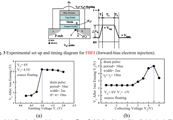
Fig. 4 (a) Changing the emitting voltage at T1 to find the best bias condition for injection in Fig. 3. (b)
Changing the collecting voltage to find the best bias condition for V2 in Fig. 3. After 4.5V, VT is dropping since the lateral field dominates the mechanism of motion of electrons.
Injection Scheme for Electrons- FBEI
For electron injection as shown in Fig.3, called forward-bias assisted electron injection (FBEI), similar to PASHEI in [9], is developed. Initially, the source, drain, and gate are grounded, during time T1, a negative voltage is applied at the drain, where
electrons are generated due to forward bias drain/substrate p-n+ diode. During time T2,
both gate and drain are switched to positive bias, then, electrons are accelerated toward the drain and reach the nitride layer via the vertical field. Fig. 4(a) shows the VT with
respect to the emitting voltage V1during T1, in which V1= -1.0V is sufficient to reach a
stable VT. Fig. 4(b) determines the collecting voltage V2 during T2, which reaches the
2 3 4 5 6 7 8 -1 0 1 2 3 4 5 V top = 5V Vtop = 6V V top = 7V 'V B(= Vtop-Vbase) (V) Th re sh old V o lta g e Sh if t ' VT (V ) + Vtop t = 0 + Vbase ϦVB T1 T2 T3 0V + Vtop t = 0 + Vbase ϦVB T1 T2 T3 0V 2 3 4 5 6 7 8 -1 0 1 2 3 4 5 V top = 5V Vtop = 6V V top = 7V 'V B(= Vtop-Vbase) (V) Th re sh old V o lta g e Sh if t ' VT (V ) + Vtop t = 0 + Vbase ϦVB T1 T2 T3 0V + Vtop t = 0 + Vbase ϦVB T1 T2 T3 0V + Vtop t = 0 + Vbase ϦVB T1 T2 T3 0V + Vtop t = 0 + Vbase ϦVB T1 T2 T3 0V VTsaturates
for pulse width longer than 1µsec 10n 100n 1u 10u 100u 1m 0 1 2 3 4 5 6 Pulse Width (s) T h reshold Vol tage V T (V) Vtop= 5V Vbase= 1V + Vtop t = 0 + Vbase ϦVB T1 T2 T3 0V + Vtop t = 0 + Vbase ϦVB T1 T2 T3 0V VTsaturates
for pulse width longer than 1µsec
VTsaturates
for pulse width longer than 1µsec 10n 100n 1u 10u 100u 1m 0 1 2 3 4 5 6 Pulse Width (s) T h reshold Vol tage V T (V) Vtop= 5V Vbase= 1V + Vtop t = 0 + Vbase ϦVB T1 T2 T3 0V + Vtop t = 0 + Vbase ϦVB T1 T2 T3 0V VS= VD= floating P-sub Ploy Si Gate S D Top Oxide Nitride Tunnel Oxide VB: pulse electron hole (T3) (T1) VS= VD= floating P-sub Ploy Si Gate S D Top Oxide Nitride Tunnel Oxide VB: pulse electron hole (T3) (T1) + Vtop t = 0 + Vbase ϦVB T1 T2 T3 0V + Vtop t = 0 + Vbase ϦVB T1 T2 T3 0V VS= VD= floating P-sub Ploy Si Gate S D Top Oxide Nitride Tunnel Oxide VB: pulse electron hole (T3) (T1) VS= VD= floating P-sub Ploy Si Gate S D Top Oxide Nitride Tunnel Oxide VB: pulse electron hole (T3) (T1) 0.0 -0.5 -1.0 -1.5 -2.0 -2.5 2 3 4 5 6 Emitting Voltage V1 (V) VT Af ter 1 m s Er asin g (V) drain pulse: period= 10us width= 2us tf= tr= 10ns VG= 6V V2= 4.5V source floating 0 1 2 3 4 5 0 1 2 3 4 5 6 VT Af ter 1m s E rasing V T (V ) drain pulse: period= 10us width= 2us tf= tr= 10ns Collecting Voltage V 2(V) VG= 6V V1= -1V source floating
1 10 100 1000 1000 2 3 4 5 6 Program: Vtop= 5V V base= 1V VG= 0V pulse width= 0.3us S= D= floating T h resh o ld Vo lt ag e VT (V) Cycle Times Erase: 1ms VG= 6V Drain:V2= 4.5V V1= -1V S= floating VB= 0V Pulse period: T1= 2us T2= 8us 1 10 100 1k 10k 100k 1M 10M 100M 1G 0 1 2 3 4 5 6 T=25°C Vtop= 5V Vbase= 1V
top pulse width= 0.3us
1ms erasing T1= 2us VG= 6V drain pulse: V1= -1V V2= 4.5V S floatingVB= 0 Thr eshold V o ltage V T (V) Retention Time (s) 10 years window ~2.8V
maximum VT when V2= 4.5V. Fig. 5 shows the transient characteristics by using the
scheme in Fig. 3, in which higher gate voltage gives faster injection speed as expected.
Fig. 5 Transient behavior of electron injection
for various gate and drain biases.
Demonstration of 1Bit and 2Bit Operations
Through different combinations of the hot hole injection and hot electron injection, different applications of the SONOS cell with 1bit/cell or 2bits/cell can be implemented.
Performance and Reliability of 1bit/cell
In the first experiment, to demonstrate a negative logic operation by using BB-HHI for program to the logic-1 state and FBEI for erase to the logic-0 state, Fig. 6(a) shows the endurance test up to 104 P/E cycles, in which no window closure can be seen and a larger operation window around 3.2V can be achieved. Fig. 6(b) shows the data retention at room temperature and a fairly large VT window (~2.8V) can be maintained after 10
years. It will be easy to meet the industry requirement. For the positive logic, these schemes are also feasible by using FBEI for programming and BB-HHI for erase, with a sacrifice of the programming speed.
(a) (b)
Fig. 6 (a) The endurance characteristics after long term P/E cycling. A large window 3.2V can still be
maintained after the cycling for 1bit/cell operation. (b) Data retention characteristic after 104 cycling at room-temperature, where 2.8V window can be maintained after 10 years.
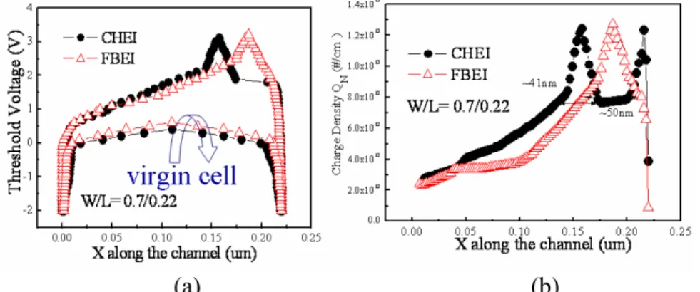
(a) (b)
Fig. 7 (a) The VT distributions of one bit for FBEI and CHEI. As shown, along the channel, FBEI VT peak
is closer to the drain than CHEI. (b) The charge density distribution along the channel. Note that FBEI is more localized toward the drain.
1E-5 1E-4 1E-3 2 3 4 5 6 VG= 6 V2= 4V VG= 6 V2= 4.5V VG= 7 V2= 4.5V Programming Time (s) Th re sh o ld Vo lta ge V T (V) Vwidth= 2us1= -1V period= 10us Logic-0 Logic-1
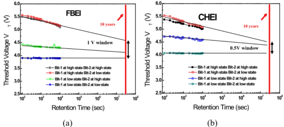
102 103 104 105 106 107 108 2.5 3.0 3.5 4.0 4.5 5.0 5.5 6.0
Bit-1 at low state Bit-2 at low state Bit-1 at low state Bit-2 at high state Bit-1 at high state Bit-2 at low state Bit-1 at high state Bit-2 at high state
T hr e sho ld V ol tage V T (V )
Retention Time (sec) FBEI 10 years 1 V window 102 103 104 105 106 107 108 2.5 3.0 3.5 4.0 4.5 5.0 5.5 6.0
Bit-1 at low state Bit-2 at low state Bit-1 at low state Bit-2 at high state Bit-1 at high state Bit-2 at low stateBit-1 at high state Bit-2 at high state
T hr es hol d V ol tage V T (V )
Retention Time (sec)
CHEI
10 years
0.5V window
Performance and Reliability of 2bit/cell
In the second experiment, combination of FBEI for program and BB-HHI for erase is also feasible for 2-bit operation. Fig. 7(a) shows the extraction of VT profile by the CP
technique [10-11] along the channel. It shows further the charge distribution, Fig. 7(b), which we can see the FBEI programmed charges are much closer to the drain in comparison to the CHEI programming.
Fig. 8 shows the bit-2 transient for FBEI and CHEI after bit-1 is programmed. Although CHEI has faster bit-1 programming speed, longer bit-2 programming time (~10m sec) is needed. Furthermore, using FBEI programming, it only needs ~1m sec reaching to the same high state as bit-1. In other words, shorter time is needed using the FBEI to program bit-2, compared to the CHEI programming. The physical mechanism why CHEI needs more programming time than FBEI shown in Fig. 8 is that the trapped charges at bit-1 will affect the charge inversion and acceleration in the channel near the drain side, such that the CHEI bit-2 programming time is longer.
Fig. 8 The bit-2 transient for FBEI and CHEI after bit-1 is programmed. We can observe that bit-2
programmed by FBEI can reach the same threshold voltage as bit-1 in shorter time compared to CHEI. The data retention after cycling is shown in Figs. 9(a) and 9(b), where an acceptable value of the four different states is achieved after 10 years. As we can see, FBEI still has 1V window after ten years in Fig. 9(a) which is larger than the window of CHEI retention (~0.5V) in Fig. 9(b). More importantly, from the data retention behavior, it shows that less damage is incurred using the FBEI scheme.
(a) (b)
Fig. 9 The retention behaviors after 10k P/E cycles for four different states in a 2bits/cell operation. The
programming mechanisms (a) FBEI and (b) CHEI , respectively. Obviously, with the use of FBEI program scheme, at least 1V window after 10 years can still be maintained.
In summary, reliable low voltage and high speed operation schemes have been demonstrated for NOR-type SONOS flash memory applications. Two different schemes have been developed for 1bit/cell and 2bit/cell operations respectively. Tunnel oxide thickness is not an issue for the future scaling using appropriate low voltage operation scheme, even without the need of using high-k in the ONO layer. In the demonstrated experiments, for a thick tunnel oxide (50Ao), a relatively low operation voltage (~5V) and excellent data retention can be preserved. It lies in the fact that a lower voltage operation will induce much less trap damage which then gives rise to a better data retention capability.
Acknowledgments
This work was supported in part by the National Science Council, Taiwan, under contract
NSC95-2221-E009-280 and MoE ATU program, National Chiao Tung University.
References
1. J. Brewer and M. Gill, Nonvolatile Memory Technologies with Emphasis on Flash, IEEE Press (2008).
2. B. Eitan et al., in IEEE EDL, 21, 543 (2000).
3. X. Wang, J. Liu, W. Bai, and D.-Lee Kwong, in IEDM Tech. Digest, 579 (2004). 4. Y. Shin, J. Choi, et al., in IEDM Tech. Digest, 327 (2005).
5. T. S. Chen et al., in IEEE EDL, 25,205 (2004). 6. S. -C. Lai et al., in IEDM Tech. Digest, 101 (2008). 7. S. S. Chung et al., in IEDM Tech. Digest, 457 (2007). 8. J. -H. Kuo et al., in Extended Abs. SSDM, 828 (2008). 9. Z. Liu et al., in Symp. on VLSI Tech., 17, (1999). 10. H. Pang et al., Proceedings of ESSDERC, 2.C.4 (2005). 11. M. Rosmeulen et al., Solid-State Electronics, 1525 (2004).