國立交通大學
電子物理系
碩 士 論 文
利用兆赫波時析光譜研究摻碲硒化鎵晶體在不同温
度下之電磁特性
Study the Electromagnetic Properties in GaSe:Te Crystals at Various
Temperatures by Terahertz Time-Domain Spectroscopy
研 究 生:麥潤東
指導教授:羅志偉 教授
利用兆赫波時析光譜研究摻碲硒化鎵晶體在不同温度下之電磁特性
Study the Electromagnetic Properties in GaSe:Te Crystals at Various
Temperatures by Terahertz Time-Domain Spectroscopy
研 究 生:麥潤東 Student : Ion-Tong Mak 指導教授:羅志偉 Advisor : Chih-Wei Luo
國 立 交 通 大 學 電 子 物 理 系
碩 士 論 文
A Thesis
Submitted to Department of Electrophysics National Chiao Tung University
in partial Fulfillment of the Requirements
for the Degree of Master
in Electrophysics
June 2010
Hsinchu, Taiwan, Republic of China 中華民國九十九年六月
i 利用兆赫波時析光譜研究摻碲硒化鎵晶體在不同温度下之電磁特性 學生:麥潤東 指導教授:羅志偉 國立交通大學電子物理系(研究所)碩士班 摘 要 在本論文中,利用自行架設之兆赫波時間解析光譜系統對摻碲硒化錠 晶體進行不同温度的量測,進而獲得 0.2 THz 至 2.5 THz 電磁波段範圍內 之複數折射率,吸收係數和介電常數。除此之外,晶體中層與層間在 0.585 THz 的剛性層振動模態將隨著碲摻雜而漸漸受到破壞,取而代之的為 1.766 THz 的晶體層內振動模態。另外,藉由聲子模態隨温度變化中出現的藍移現 象可以進一步驗證和解析碲在硒化鎵晶體中所扮演的角色。
ii
Study the Electromagnetic Properties in GaSe:Te Crystals at Various Temperatures by Terahertz Time-Domain Spectroscopy
Student : Ion-Tong Mak Advisor : Chih-Wei Luo
Department of Electrophysics National Chiao Tung University
ABSTRACT
Since the tellurium-doped gallium selenide crystals has good potential in phase-matching applications, the homemade terahertz time-domain spectroscopy technique is employed to investigate the physical properties like complex refractive indices and absorption coefficients within the electromagnetic wave range of 0.2 THz to 2.5 THz. The deformation of the rigid layer mode at 0.58 THz, and the formation of the tellurium-induced layer vibrational mode at 1.76 THz were clearly observed in absorption spectra. Moreover, the role of tellurium-doping in GaSe crystals could be revealed from the temperature-dependent blue shift of the rigid layer mode and tellurium-induced layer vibrational mode.
iii
Acknowledgement
Imminent comes the graduation, I’ve spent six years in Taiwan for higher education, including four years of undergraduate education and two years of master degree research. As an adult, I’ve been continuously studying how to judge right and wrong and how to express well, I want to thank for everyone I knew. We always make friends with others, we learn against the bad friends and cheer with the closed, I am grateful to Wei-Tsung Tang who used to be a respectable friend, Hsuan-I Wang who is thoughtful and won't miss any important thing for friends, Chi-Him Tang who is kind and honest, and the others. For the research, I’d like to thank you for all members in UDL, especially my advisor Chih-Wei Luo who have the insights of the physics problems, senior student Hsun-Chuan Shih who establish the whole framework of the experiment system, Shin-An Ku who maintains the system well and teach me a lot, Wei-Chen Chu who prepare the samples well for me, and I also owe the care of the junior students like Chih-Hsiang Su and Chia-Ching Lee, etc.. Moreover, I have to thank you for the supplement by Professor Yury M. Andreev from the institute of monitoring of climatic and ecological systems in Russia.
iv
Table of Content
Page Chinese Abstract……….………... i English Abstract………... ii Acknowledgement……….……….. iii Table of Contents……….…….... iv List of Tables………..………. viList of Figures………...………... vii
I. Introduction………...………… 1
II. Electromagnetic Principles………...………… 6
2.1 Electromagnetic Waves in Crystals…….………...……….... 6
2.2 Power Spectra………..………...………… 8
2.3 Complex Refractive Index………...……….………... 8
2.4 Absorption Coefficient……….……….... 10
2.5 Dielectric Responses………. 10
III. Experiments……...………... 12
3.1 Sample Preparation………..………. 12
3.2 THz Time-Domain Spectroscopy System……..……….. 12
3.3 The Principles for THz Generation and Detection………...………… 14
IV. Results and discussion…………..……… 17
4.1 The Characteristics of GaSe:Te Crystals at Room Temperature..….... 17
4.1.1 Complex Refractive Indices……… 21
4.1.2 Absorption Coefficients………….………. 25
4.2 The Characteristics of GaSe:Te Crystals at Low Temperatures...…… 29
v
Page 4.2.2 The Variation of Phonon Modes in Absorption Spectra..…… 31 4.2.3 Dielectric Responses..………... 35 V. Summary and Prospect………... 38 VI. References……… 39
vi
List of Tables
Page Table 1 Electrical and optical parameters of doped GaSe……… 3 Table 2 Doping level and the thickness of GaSe1-xTex crystals...………... 12
Table 3 Vibrational modes calculated by the First Principle……….. 20 Table 4 The fitting parameters used in the Sellmeier formula for the
experimental data of refractive indices in GaSe1-xTex……… 24
vii
List of Figures
Page Figure 1 (a) SEM picture of the GaSe1-xTex layer structure; (b) Atomic structure
of ε-type GaSe; (c) Atomic structure of β-type GaTe……….. 2 Figure 2 The transmittance of GaSe1-xTex…..………..……… 4
Figure 3 Schematic diagram of THz time-domain spectroscopy system……... 13 Figure 4 (a) Time-domain spectrum of various GaSe1-xTex samples; (b)
Time-domain spectrum of a GaSe0.9994Te0.0006 crystal at various temperature………...… 15 Figure 5 Frequency domain spectra of GaSe1-xTex crystals…………...………. 18
Figure 6 Transmittance spectra of GaSe1-xTex crystals….……….. 18
Figure 7 (a) Configuration of the rigid layer vibrational mode; (b) Configuration of the vibrational mode at 56.8 cm-1………. 19 Figure 8 (a) Real part and (b) Imaginary part of the ordinary refractive indices
GaSe1-xTex crystals with thickness >0.75 mm at room temperature; (c)
Real part of the ordinary refractive indices in the GaSe1-xTex thin
crystals around 0.3 mm………...……….. 22 Figure 9 (a) Real part of the refractive index of pure ε-type GaSe crystal at room
temperature and the Sellmeier formula fitted curve; (b) Real part of the refractive index of GaSe0.9988Te0.0012 crystal at room temperature
and the Sellmeier formula fitted curve………...……… 24 Figure 10 Absorption coefficients of GaSe1-xTex at room temperature…...…... 25
Figure 11 Stacked absorption curves of GaSe1-xTex………...……… 25
Figure 12 Vibrational modes’ representations of the pure ε-type GaSe crystal. 26 Figure 13 The Raman Spectra for (a) the pure ε-type GaSe crystals; (b) the
viii
Page Figure 14 Peak changes of the rigid layer mode..……….. 28 Figure 15 Peak changes of the Te impurity induced mode……….… 28 Figure 16 The temperature-dependent real part of the ordinary refractive indices of GaSe1-xTex crystals with Te mass percentage (a) 0.00%; (b) 0.05%;
(c) 0.10%; (d) 0.50%; (e) 1.00%; (f) 2.00%, where the y-axis is on the right side of the graph... 30 Figure 17 The real part of the ordinary refractive indices are simulated by the
Eq. (4.5) at various temperatures………...…...……...…. 31 Figure 18 The temperature-dependent absorption spectra of GaSe1-xTex crystals
with Te mass percentage (a) 0.00%; (b) 0.05%; (c) 0.10%; (d) 0.50%; (e) 1.00%; (f) 2.00%, where the y-axis is on the right side of the graph………..………... 32 Figure 19 The frequency of (a) rigid layer mode and; (b) Te-induced mode as a
function of temperature………..………... 34 Figure 20 Real part of dielectric coefficients in GaSe1-xTex crystals at room
temperature……….……….. 35 Figure 21 Imaginary part of dielectric coefficients in GaSe1-xTex crystals at room
temperature………..……….……… 35 Figure 22 The temperature-dependent real parts of dielectric coefficients in
GaSe1-xTex crystals with Te mass percentage (a) 0.00%; (b) 0.05%; (c) 0.10%; (d) 0.50%; (e) 1.00%; (f) 2.00%... 36 Figure 23 The temperature-dependent imaginary parts of dielectric coefficients
in GaSe1-xTex crystals with Te mass percentage (a) 0.00%; (b) 0.05%; (c) 0.10%; (d) 0.50%; (e) 1.00%; (f) 2.00%... 37
- 1 -
I. Introduction
Semiconductors are so common nowadays due to the wide applications such as the chipsets inside the cell-phones, the micro-FET components in the integrated circuits or the luminous semiconductor devices. Besides the well known applications in the electronics, semiconductors also play and important role in the applications of nonlinear optics, e.g. GaSe, ZnTe, etc.. In particular, the III-VI class semiconductors gallium selenide (GaSe) are the important nonlinear crystals for mid-IR generation, which have good characters such as the high nonlinear susceptibility χ(2)(𝑑22 = 54 𝑝𝑚/𝑉) and anisotropy. Although there are four crystalline types in GaSe structure, ε-, β-, γ-, δ-type [1], the layered ε-type is the most stable structure among them for GaSe compound as shown by the SEM image in Fig. 1(a). Fig. 1(b) further illustrates that one layer comprises of four atomic planes (Se-Ga-Ga-Se along c-axis) and bound with each other by the ionic bonds (white bar). Also, these layers are bounded by the Van der Waals force to form a layered-structure crystal.
- 2 -
The pure III-VI gallium selenide crystals had been studied in the 1960s. Until the 1970s, the optical and electrical characteristics of the pure or doped III-VI semiconductor were observed [2,3,4] because of the development of the instruments [5]. For instance, the mobility, the carrier concentration, the band structures, the band edge absorption, and the luminance properties were continuously reported in some journals [6,7,8,9]. After the quiet 1980 ages, the nonlinear effect in pure and doped GaSe crystals was attracted the researchers’ attention again [10,11,12,13,14,15] especially for the applications in phase-matching, e.g. the different frequency generation, the sum frequency emission, the optical parametric oscillator, or even the optical parametric amplifier.
Fig. 1 (a) SEM picture of the GaSe:Te layer structure; (b) Atomic structure of ε-type GaSe;
(c) Atomic structure of β-type GaTe
- 3 -
Dopant In Al S Te
Doping level (mass %) 0.01-3 0.01-3 0.01-3 0.01-3
Supposed predominant dopant introduction in the GaSe crystal
To Ga sites and interlayer space: donor, compensates the material, hardens the crystal To interlayer space: donor, compensates the material, hardens the crystal and Ga
sites: substitutes Ga vacancies, enhances layer structure To Se sites: homogenizes the crystal, brings GaS structure close to GaSe and interstitials, acceptor, worsens layer structure To the Se sites: leads to structure disorders in the crystal
Conduction type of the doped
crystals Hole Hole Hole Hole
Electrical properties (300 K) σ(𝑂ℎ𝑚−1∗ 𝑐𝑚−1 for GaSe 3.5 ∙ 10−3~1 ∙ 10−2) 2 ∙ 10−3~2 ∙ 10−2 1 ∙ 10 −7 1.5 ∙ 10−4 1.4 ∙ 10−4 μ (𝑐𝑚−1/𝑉 ∙ 𝑠 for GaSe 20~23) 20 100~200 3 13 p (𝑐𝑚−3 for GaSe 1 ∙ 1015~5 ∙ 1015) 5 ∙ 1014~5 ∙ 1015 2.5 ∙ 10 15 1 ∙ 1014 6 ∙ 10−13 Optical properties (300 K) Transparency range (GaSe 0.62~18 μm, 𝐸𝑔 = 1.95 𝑒𝑉) 0.62~18 μm, 𝐸𝑔= 1.95𝑒𝑉 0.62~17 μm, 𝐸𝑔= 1.95 𝑒𝑉 0.62~18 μm, 𝐸𝑔= 2.06 𝑒𝑉 0.62~18 μm, 𝐸𝑔= 1.85𝑒𝑉
Type of photoconductivity and its
main features - Intrinsic, band broadens to 300~680 μm Intrinsic within 400~600 nm + two impurity bands at 600~900 and 900~1700 nm Intrinsic at 400~650 nm + two impurity bands 650~900 and 900~1700 nm Absorption peak appears at (eV) - 0.06 ad 0.26 0.36 and 0.41 0.12~0.14 Microhardness rises up to (kg/𝑚𝑚2,
~8 for GaSe) 14 20 17 10
- 4 -
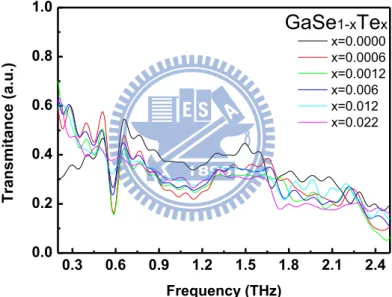
In order to compare the properties of GaSe:Te with other doping elements, some of the parameters have been listed in Table 1 [16, 17]. The transmittance of the Te-doped GaSe crystals in visible range is shown in Fig. 2. The optical absorption band edge of GaSe crystals locates at around 620 nm (photon energy of 2.00 eV), while the GaTe crystals locate at 753 nm (photon energy of 1.65 eV). Thus it is benefited that the band gap energy can be modified within the range of 1.65 eV~2.00 eV if the tellurium atoms are doped into the GaSe crystals or the selenium atoms are doped into the GaTe crystals. Indeed, the transmission edge significantly shifts to longer wavelength as increasing the concentration of Te in GaSe:Te crystals..
400 500 600 700 800 0 20 40 60 3 2.5 Photon Energy(eV)2 1.5 T ra n smis sion (%) Wavelength(nm) x=0.0006 x=0.0012 x=0.006 x=0.012 x=0.022
GaSe
1-xTe
xSome important applications of the GaSe crystals are the type-I and the type-II phase-matching for the mid- to far-IR generation. In ref. [14], a BBO-based optical parametric oscillator and a Nd:YAG laser were used to perform the difference frequency generation of mid-infrared in pure ε-type GaSe crystals. In particular, the refractive indices of the pure GaSe at the far- and
- 5 -
mid-infrared region were studied in order to assure the possibility of the system construction. In spite of its many attractive features, for generation from near to mid infrared and further to terahertz range, the GaSe crystals is difficult to be cut and polished along some arbitrarily chosen directions. For the applications in optics, further improvement in the optical and mechanical properties of the GaSe crystals is highly desirable. The doping of GaSe crystals seems to be the most economical way to radically improve its mechanical and other physical properties. Recent developments in the crystal growth technology indicated that GaSe can be doped with several elements, e.g. Er, Al, In, S, and Te, to strengthen the structural properties and noticeably modify the optical properties. Comparing with Er-, Al-, In-, S-doping, the Te-doped GaSe crystals are benefited by the high power THz generation with type-II phase-matching in the mid-IR region [17]. Thus, we use the time-domain spectroscopy technique to investigate the characteristics of the Te-doped ε-type GaSe crystals in the far-infrared frequency region. Moreover, the temperature-dependent measurements in time-domain spectroscopy will provide us more information about the role of Te-doping in the GaSe crystals.
- 6 -
II. Principle
After obtaining the time-domain signals, it can be converted to the frequency domain spectra through the Fast-Fourier Transform. Owing to both amplitude and phase information have been simultaneously included in the time-domain signals [18], we can directly obtain the electromagnetic properties without Kramers-Kronig relations. In this chapter, we will describe the principle and procedure for calculating the complex refractive indices, the absorption coefficients, and the complex dielectric responses from time-domain signals.
2.1 Electromagnetic Waves in Crystals
When the electromagnetic wave straightly penetrates through the crystals, a time delay will be created due to its different optical path length between the crystals and the surrounding. The delay time is
∆𝑡 =(𝑛𝑆𝑎𝑚𝑝𝑙𝑒−1)𝑑
𝑐 (2.1)
where 𝑛𝑆𝑎𝑚𝑝𝑙𝑒 is the refractive index of the sample, 𝑑 is the thickness of the sample, 𝑐 is the speed of light.
The propagation process can be described by the spectral components, either 𝑆(𝑡) in the time domain or 𝑆(𝜔) in the frequency domain. The propagation wave is influenced by the reflectance and the transmittance of both surfaces of a crystal,
- 7 - 𝑆𝑆𝑎𝑚𝑝𝑙𝑒(𝜔) = 𝑡12(𝜔) ∙ 𝑡23(𝜔) ∙ 𝑝2(𝜔, 𝐿) ∙ ∑ *𝑟23(𝜔) ∙ 𝑝22(𝜔, 𝐿) ∙ 𝑟 21(𝜔)+𝑘 ∞ 𝑘=0 ∙ 𝐸(𝜔) (2.2) 𝑆𝑅𝑒𝑓(𝜔) = 𝑡13(𝜔)∙𝑝1,3(𝜔, 𝐿)∙ 𝐸(𝜔) (2.3) where 𝑆𝑆𝑎𝑚𝑝𝑙𝑒(𝜔) is the spectral component through sample; 𝑆𝑅𝑒𝑓(𝜔) is the spectral component without sample; 𝑡12(𝜔) and 𝑡23(𝜔) are, respectively, the
transmission coefficients through the surface and the rear surface (the suffixes 1, 2, and 3 represent medium 1, medium 2, and medium 3 respectively); 𝑟23(𝜔) and 𝑟21(𝜔) are, respectively, the backward reflection coefficients of the rear and the front surfaces; 𝑝2(𝜔, 𝐿) and 𝑝1,3(𝜔, 𝐿) are, respectively, the propagation coefficients inside and outside the sample over the distance 𝐿, 𝐸(𝜔) is the electric field of the propagation wave. In normal incidence electromagnetic wave, the transmissions, reflection, and propagation coefficients between medium a and medium b are derived to be
𝑡𝑎𝑏(𝜔) = 2𝑛̃𝑎 𝑛̃𝑎+𝑛̃𝑏 (2.4) 𝑟𝑎𝑏(𝜔) = 𝑛̃𝑎−𝑛̃𝑏 𝑛̃𝑎+𝑛̃𝑏 (2.5) 𝑝𝑎(𝜔, 𝑑) = exp ,𝑖𝑛̃𝑎𝜔𝑑 𝑐 - (2.6)
For the case of thick sample, the second reflection signal locates far from the primitive one, the multi-reflection and the summation effects of Fabry-Perot can be neglected.
- 8 -
2.2 Power Spectrum
The Fourier transform between the power spectra in the time domain and the frequency domain is represented by
𝑃̃(𝜔) = 𝐴(𝜔) 𝑒𝑥𝑝,−𝑖𝜑(𝜔)- = ∫ 𝑃(𝑡) 𝑒𝑥𝑝(−𝑖𝜔𝑡) 𝑑𝑡 (2.7) where 𝑃̃(𝜔) and 𝑃(𝑡) are, respectively, the power spectra in the frequency domain and the power spectra in time domain, meanwhile they are proportional to the spectral components 𝑆(𝜔) and 𝑆(𝑡) respectively; 𝐴(𝜔) and 𝜑(𝜔) are the amplitude and the phase of the power spectrum respectively.
2.3 The Complex Refractive Index
The ratio of the two spectral components, which means the total transmission coefficient of the samples, will lead the derivation to the complex refraction index, 𝑆𝑆𝑎𝑚𝑝𝑙𝑒(𝜔) 𝑆𝑅𝑒𝑓(𝜔) = 𝑡12(𝜔)∙𝑡23(𝜔)∙ 𝑒𝑖 𝑛 ̃𝜔𝑑 𝑐 𝑒𝑖 𝜔𝑑 𝑐 = 𝜌𝑒𝑖∆𝜑 (2.8)
the ratio of the exponential terms corresponds to the delay time and 𝑡 = 𝑡12(𝜔)∙𝑡23(𝜔) is the transmittance of the samples; 𝜌 is the amplitude of the
ratio and ∆𝜑 is the phase difference of spectral components. Medium 1 and 3 are free space or air, whose refractive indices are approximated to be 1. Medium 2, the sample, whose complex refractive index is represented by 𝑛̃ = 𝑛 + 𝑖𝑘. Thus, some simplifications of the ratio can take place,
- 9 - 𝜌𝑒𝑖∆𝜑 = 𝑡12(𝜔) ∙ 𝑡23(𝜔) ∙𝑒 𝑖𝑛̃𝜔𝑑𝑐 𝑒𝑖𝜔𝑑𝑐 = 2 ∙ 1 1 + 𝑛̃∙ 2𝑛̃ 𝑛̃ + 1∙ 𝑒 𝑖(𝑛̃−1)𝜔𝑑𝑐 = 4(𝑛 + 𝑖𝑘) (𝑛 + 𝑖𝑘 + 1)2∙ 𝑒 𝑖(𝑛−1)𝜔𝑑𝑐 ∙ 𝑒−𝑘𝜔𝑑𝑐 = 4(𝑛 + 𝑖𝑘),(𝑛 + 1) 2− 𝑘2 + 𝑖2(𝑛 + 1)𝑘-,(𝑛 + 1)2− 𝑘2+ 𝑖2(𝑛 + 1)𝑘-,(𝑛 + 1)2− 𝑘2− 𝑖2(𝑛 + 1)𝑘-∙ 𝑒𝑖(𝑛−1)𝜔𝑑𝑐 ∙ 𝑒− 𝑘𝜔𝑑 𝑐 =4*𝑛,(𝑛 + 1) 2− 𝑘2- + 2(𝑛 + 1)𝑘2+ − 𝑖*2𝑛(𝑛 + 1)𝑘 − 𝑘,(𝑛 + 1)2− 𝑘2-+ ,(𝑛 + 1)2− 𝑘2-2+ 4(𝑛 + 1)2𝑘2 ∙ 𝑒𝑖(𝑛−1)𝜔𝑑𝑐 ∙ 𝑒− 𝑘𝜔𝑑 𝑐 = 4(𝑛 + 1)3{[ 𝑛 𝑛 + 1 − 𝑛𝑘2 (𝑛 + 1)3+ 2 𝑘2 𝑛 + 1] − 𝑖 [2 𝑛𝑘 (𝑛 + 1)2− 𝑘 (𝑛 + 1)2+ 𝑘3 (𝑛 + 1)3]} (𝑛 + 1)4[1 − . 𝑘 𝑛 + 1/ 2 ] 2 ∙ 𝑒𝑖(𝑛−1)𝜔𝑑𝑐 ∙ 𝑒− 𝑘𝜔𝑑 𝑐 (2.9)
If the refractive index of the samples has the discrepancy of n + 1 ≫ k, the above ratio would converge to a closed form that both the real part and the imaginary part of the refractive indices can be obtained by comparison.
𝜌𝑒𝑖∆𝜑 ≅ 4𝑛 (𝑛+1)2∙ 𝑒 −𝑘𝜔𝑑 𝑐 ∙ 𝑒𝑖 (𝑛−1)𝜔𝑑 𝑐 (2.10)
Thus the real part of refractive index is n ≅ 1 +𝑐∆𝜑
𝜔𝑑 (2.11)
and the imaginary part is k ≅ 𝑐
𝜔𝑑ln , 4𝑛
- 10 -
2.4 Absorption Coefficient
The strength of the penetration wave between two surfaces of a sample experiences a decay, which is
P3′(𝜔) = P1′(𝜔)exp,−αd- (2.13)
P1′(𝜔) here is the strength just behind the first incident surface. After the wave propagates and decays over a distance 𝑑 , the output strength is P3′(𝜔). Moreover, α is defined as the absorption coefficient, whose unit is cm-1
and magnitude is related to the transmittances as,
α = 1 𝑑ln ( P1′(𝜔) P3′(𝜔)) = 1 𝑑ln (𝑇23𝑇12 P1(𝜔) P3(𝜔)) (2.14)
For the transparent sample, the absorption coefficient can be estimated from the sample thickness and the transmittance.
2.5 Dielectric Responses
In the electromagnetism, the Maxwell equations for EM-wave propagating in the conducting material are different from those equations for EM-wave propagating in vacuum, { ∇ ∙ 𝐸⃑ = 0 ∇ ∙ 𝐵⃑ = 0 ∇ × 𝐸⃑ = −𝜇𝜕𝐻⃑⃑ 𝜕𝑡 ∇ × 𝐻⃑⃑ = 𝜍𝐸⃑ + 𝜀𝜕𝐸⃑ 𝜕𝑡 (2.15)
the Laplace equation is thus derived to be
−∇2𝐸⃑ = ∇ × ∇ × 𝐸⃑ − ∇ ∙ (∇ × 𝐸⃑ ) = ∇ × ∇ × 𝐸⃑ (2.16) And
- 11 - ∇ × ∇ × 𝐸⃑ = ∇ × .−𝜇𝜕𝐻⃑⃑ 𝜕𝑡/ = −𝜇 𝜕 𝜕𝑡(∇ × 𝐻⃑⃑ ) = −𝜇 𝜕 𝜕𝑡(𝜍𝐸⃑ + 𝜀 𝜕𝐸⃑ 𝜕𝑡) = −μσ∂𝐸⃑ ∂t − 𝜇𝜀 𝜕2𝐸⃑ 𝜕𝑡2 (2.17)
The velocity relation of the propagating plane wave E = 𝐸0𝑒−𝑖𝜔(𝑡−𝜔𝑣) = 𝐸0𝑒𝑖(𝑘𝑥−𝜔𝑡) to the Laplace equation is
1
𝑣2 = 𝜇𝜀 − 𝑖
𝜎𝜇
𝜔 (2.18)
The complex refractive index is related to the velocity of light and the wave propagation velocity in the medium; or it is related to the electric permittivity 𝜀̃ and the magnetic permeability 𝜇̃. Thus we can obtain the relation 𝑛̃2 = 𝑐2 ∙ 1
𝑣2 and 𝑛̃2 = 𝜀̃ ∙ 𝜇̃. For the GaSe sample which is the non-magnetic material with 𝜇̃ ≅ 1, it only relates to the dielectric function,
𝑛̃2 = 𝑐2(𝜇𝑟𝜀𝑟𝜇0𝜀0+ 𝑖 𝜍𝜇𝑟𝜇0⁄ ) = 𝜇𝜔 𝑟𝜀𝑟 + 𝑖 𝜍𝜇𝑟⁄𝜔𝜀0
≅ 𝜀𝑟 + 𝑖 𝜍 𝜔𝜀⁄ 0 (2.19)
𝑛̃2 = (𝑛 + 𝑖𝑘)2 = (𝑛2− 𝑘2) + 𝑖2𝑛𝑘
≅ 𝜀̃ = 𝜀1+ 𝑖𝜀2 (2.20) By comparison to Eq. (2.19) and Eq. (2.20), the real part and the imaginary part of the dielectric function are respectively
𝜀1 ≅ 𝑛2− 𝑘2 ≅ 𝜀
𝑟 (2.21)
𝜀2 ≅ 2𝑛𝑘 ≅ 𝜍 𝜔𝜀⁄ 0 (2.22)
and thus the conductivity of the material for optical frequency concerned is
- 12 -
III. Experiments
3.1 Sample Preparation
The Te-doped GaSe crystals with ε -type stacks were grown by the Bridgman technique and were supplied by Professor Yury M. Andreev of the Institute of Monitoring of Climatic and Ecological Systems, SB RAS, Tomsk in Russia. In this study, we have six sorts of the crystals, one is the pure GaSe crystal and five of them are in various doping levels. The mass doping levels and the thicknesses of them are shown in Table. 2. All of the samples used in the ordinary incidence measurements are prepared by the z-cut cleavage.
A B C D E F Doping level (mass %) 0.00 0.05 0.10 0.50 1.00 2.00 Thickness (mm) 1.30 1.38 1.22 1.39 0.96 0.75 0.00 0.0006 0.0012 0.006 0.012 0.022
3.2 THz Time-Domain Spectroscopy System
For the room temperature experiments, the THz time domain spectroscopy system can be divided mainly into three parts, i.e. the area for the samples, the area for THz wave propagation which is covered by a plastic box to keep the humidity below 6 %, and the area for laser pulses guiding as shown in the Fig. 3.
- 13 -
The input femtosecond laser pulses are split into two paths, one is the pump beam and the other is the signal beam. The THz wave is generated from the indium phosphor semiconductor antenna by the photoconductive switching effect with the pump beam. The THz wave propagates and is guided by two pairs of off-axis parabolic mirrors inside the box. The GaSe1-xTex crystals are
illuminated by the THz beam right at the focus point. Then, the signal beam passes the delay stage which provides the time resolution for THz time-domain spectroscopy. At last, the THz and femtosecond laser beams are joined to the electro-optic sampling detection part. In order to avoid the absorption of water vapor in THz range [19], moreover, the box is purged with nitrogen gas to reduce the humidity lower than 6 %.
For the measurements at various temperatures, the samples are put inside a vacuum chamber which is sealed with Teflon windows. The chamber is provided a high vacuum level of 10−6 Torr to isolate the heat flow from the environments. The temperatures of samples can be controlled from room temperature to 40 K.
- 14 -
3.3 The Principles for THz Generation and Detection
When a laser pulse of 800 nm irradiates on the indium phosphor antenna, many free carriers will be generated inside the illuminated area. With applying 180 V bias voltage to the antenna, an induced time-varying current flows between the electrodes. Then, the indium phosphor antenna radiates the electromagnetic wave [20] from the surface of antenna. The electric field of this radiated wave is proportional to the time-varying current density,
𝐸(𝑡) ∝𝜕𝐽(𝑡)
𝜕𝑡 (3.1)
Finally, the THz pulse can be generated by the femtosecond laser pulse with the peak power of 2.31 nJ and the repetition rate of 80 MHz. Furthermore, the characteristics of THz pulse could be significantly affected by the material of the antenna, the electrodes’ distance, or even the pattern of the antenna.
The electro-optic sampling detection used in this system includes a birefringence ZnTe crystal, a quarter waveplate, a Wollaston prism and a pair of photodiodes. The main idea [21] of the detecting method is that the electro-optic (or Pockels effect) and the phase retardation Γ occurs in the (110) face of a ZnTe crystal by the THz electric field at normal incidence. The phase retardation Γ can be expressed as,
Γ =𝜔𝑛03𝐸𝑇𝐻𝑧𝑟41𝐿
𝑐 (3.2)
where 𝑛0 is the refractive index of ZnTe crystal, 𝑟41 is the electro-optic coefficient and 𝐿 is the thickness of ZnTe crystal. During the pass of the signal beam (or probe beam) in a ZnTe crystal, the signal beam will be modified by the phase retardation of the ZnTe crystal caused by the THz electric field 𝐸𝑇𝐻𝑧. The polarization of probe beam will change from linear to circular through the 𝜆 4⁄
- 15 -
waveplate and the transmittance is linearly approximated with the retardation Γ. The orthogonally polarizations of the probe beam are separated by the Wollaston prism to perform the retardation detection via the differential photo diodes. The final signal, which is in the form of ∆I = ΓI ∝ 𝑆𝑇𝐻𝑧(𝜔), is sent to the lock-in amplifier with a reference frequency of 2.39 kHz.
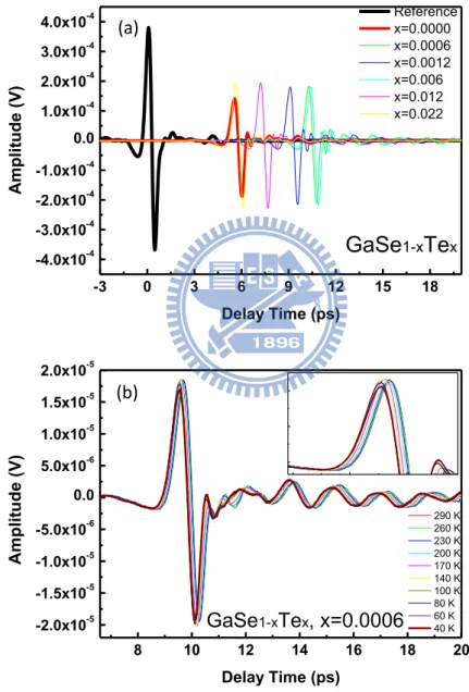
8 10 12 14 16 18 20 -2.0x10⁻⁵ -1.5x10⁻⁵ -1.0x10⁻⁵ -5.0x10⁻⁶ 0.0 5.0x10⁻⁶ 1.0x10⁻⁵ 1.5x10⁻⁵ 2.0x10⁻⁵ A m p li tu d e ( V ) Delay Time (ps) 290 K 260 K 230 K 200 K 170 K 140 K 100 K 80 K 60 K 40 K GaSe1-xTex, x=0.0006 -3 0 3 6 9 12 15 18 -4.0x10⁻⁴ -3.0x10⁻⁴ -2.0x10⁻⁴ -1.0x10⁻⁴ 0.0 1.0x10⁻⁴ 2.0x10⁻⁴ 3.0x10⁻⁴ 4.0x10⁻⁴ Am p li tu d e ( V ) Delay Time (ps) Reference x=0.0000 x=0.0006 x=0.0012 x=0.006 x=0.012 x=0.022 GaSe1-xTex
Fig. 4 (a) Time-domain spectrum of various GaSe1-xTex samples; (b) Time domain spectrum of a GaSe0.9994Te0.0006 crystal
at various temperatures (a)
- 16 -
The bold black line in Fig. 4(a) shows the typical THz signal with FWHM of about 400 fs in air. After passing through samples at room temperature, a dramatic delay related to the reference signal appears. Due to the thermo-expansion effect, e.g. the delay is also clearly observed in the signals from the GaSe0.9994Te0.0006 crystal measured at various temperatures as shown in
- 17 -
IV. Results and Discussion
Thanks to the measurements of the time-domain spectroscopy system, and then the reliable parameters of the Te-doped gallium selenide crystals can be obtained or be calculated in the far-infrared region. The complex refractive indices, the absorption coefficient, and the dielectric responses at various temperatures will be presented and discussed in this chapter. Also, some structural behaviors like the interlayer vibration and the impurity influence are concerned.
4.1 The Characteristics of GaSe
1-xTe
xCrystals at Room Temperature
Figure 5 shows the power spectra in frequency domain of GaSe1-xTex
crystals, which are obtained from the Fig. 4(a) via the Fourier transform. The bandwidth of this spectrum is about 2.3 THz (1.4 mm), i.e. from far-infrared region 2.5 THz (0.12 mm) to micro-wave region 0.2 THz (1.5 mm). The signal to noise ratio is bad elsewhere due to the amplitude of the signal drops dramatically below 0.2THz and oscillates strongly beyond 2.5 THz. According to the real part of Eq. (2.9), the transmittance spectra of various samples are obtained from Fig. 5 and shown in Fig. 6. At room temperature, all of the transmittance spectra have the same tendency, namely decrease from 60 % down to about 10 % as increasing frequency.
- 18 -
Furthermore, we found a clearly deep in the transmittance spectra which indicates that certain absorption occurs around 0.58 THz (19.3 cm-1). In general, this absorption deep is called rigid layer mode which characterizes the ε-type layered pure GaSe crystals. It is caused by the out of phase interlayer vibrations and the in-phase intralayer vibrations. The observed vibrational modes probably match with the vibrational modes indicated by the first principle calculations
Fig. 5 Frequency domain spectra of GaSe1-xTex crystals
Fig. 6 Transmittance spectra of GaSe1-xTex crystals
0.3 0.6 0.9 1.2 1.5 1.8 2.1 2.4 10-15 10-14 10-13 10-12 10-11 Am p li tu d e ( a.u.) Frequency (THz) Reference x=0.0000 x=0.0006 x=0.0012 x=0.006 x=0.012 x=0.022 GaSe1-xTex 0.3 0.6 0.9 1.2 1.5 1.8 2.1 2.4 0.0 0.2 0.4 0.6 0.8 1.0 T ra n smit an ce ( a.u.) Frequency (THz) x=0.0000 x=0.0006 x=0.0012 x=0.006 x=0.012 x=0.022 GaSe1-xTex
- 19 -
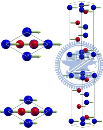
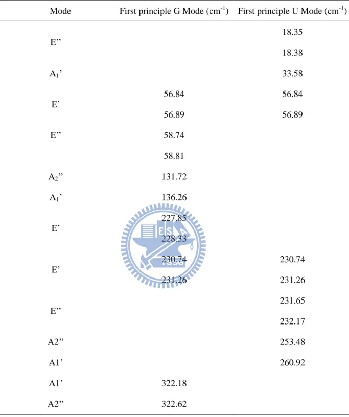
which study the physics of materials based on their compositions without experimental data. The configuration is derived by the Density Function Perturbation Theory to describe the atomic pseudo-potential variation and the different modes of phonon vibrations. The configuration of the rigid layer mode is shown in Fig. 7 [22]. There are other vibrational modes’ configurations versus different infrared vibrational frequencies and they are listed below in Table. 3
Fig. 7 (a) Configuration of the rigid layer vibrational mode at 19.3 cm-1; (b) Configuration of the vibrational mode at 56.8 cm-1
- 20 -
Mode First principle G Mode (cm-1) First principle U Mode (cm-1) E’’ 18.35 18.38 A1’ 33.58 E’ 56.84 56.84 56.89 56.89 E’’ 58.74 58.81 A2’’ 131.72 A1’ 136.26 E’ 227.85 228.33 E’ 230.74 230.74 231.26 231.26 E’’ 231.65 232.17 A2’’ 253.48 A1’ 260.92 A1’ 322.18 A2’’ 322.62
This rigid layer mode can also be observed in low-doped GaSe1-xTex
crystals. The rigid layer mode of ε-type GaSe crystals at 0.58 THz (19.3 cm-1)
- 21 -
presents in both the frequency-domain spectra and the transmittance spectra including various Te-doping levels.
4.1.1 Complex Refractive Indices
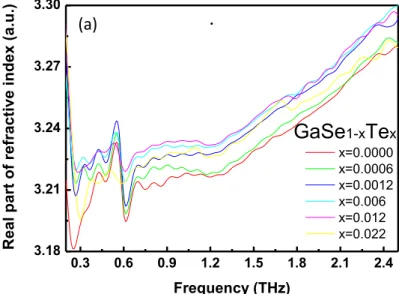
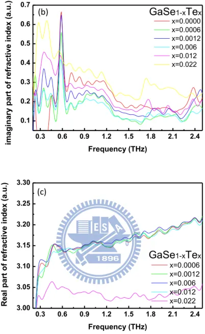
Figure 8 shows the real part and the imaginary part of the ordinary refractive indices, which were calculated from the Eq. (2.11) and Eq. (2.12). The real part of refractive index is quite flat at low frequencies except phonon mode oscillations, and it rises slowly as increasing frequencies. The value is around 3.21 at low frequency range and rises towards 3.3 due to the Transverse Optical phonon mode oscillation at 6.40 THz (46.8 μm). The rigid layer phonon mode can be clearly observed in the refractive indices’ diagrams; and this mode induces an increment in the real part of refractive index while approaching the mode center from low frequency side and then drops just behind it. Correspondingly, there is a peak appeared in the imaginary part of the ordinary refractive indices at where it represents absorption.
. 0.3 0.6 0.9 1.2 1.5 1.8 2.1 2.4 3.18 3.21 3.24 3.27 3.30 R e a l p a rt o f r e fr a c tiv e i n d e x ( a .u .) Frequency (THz) x=0.0000 x=0.0006 x=0.0012 x=0.006 x=0.012 x=0.022 GaSe1-xTex (a)
- 22 -
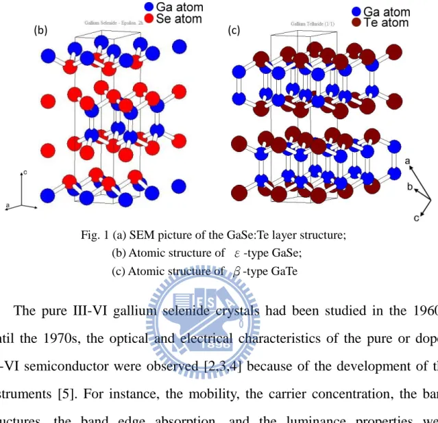
The real part of refractive indices of thick GaSe1-xTex crystals increases as
increasing the concentration of Te. For the thin GaSe1-xTex crystals, however, it
shows neither any clear dependence of the Te-doping nor any absorption modes
0.3 0.6 0.9 1.2 1.5 1.8 2.1 2.4 0.1 0.2 0.3 0.4 0.5 0.6 0.7 ima g ina ry pa rt of re fr ac tive i n d ex ( a.u.) Frequency (THz) x=0.0000 x=0.0006 x=0.0012 x=0.006 x=0.012 x=0.022 GaSe1-xTex
Fig. 8 (a) Real part and (b) Imaginary part of the ordinary refractive indices in GaSe1-xTex crystals with
thickness >0.75 mm at room temperature; (c) Real part of the ordinary refractive indices in the GaSe1-xTex thin crystals around 0.3 mm
(b) 0.3 0.6 0.9 1.2 1.5 1.8 2.1 2.4 3.00 3.05 3.10 3.15 3.20 3.25 3.30 Re al p ar t of re fr ac tive i n d ex ( a.u.) Frequency (THz) x=0.0006 x=0.0012 x=0.006 x=0.012 x=0.022 GaSe1-xTex (c)
- 23 -
as in Fig. 8(c). This may be caused by the non-uniform distribution of Te atoms in single crystal. The Sellmeier formula[10,23,24] is commonly used in the transparent region of most materials,
𝑛𝑜2 = 𝐴 + 𝐵 𝜆2+ 𝐶 𝜆4 + 𝐷 𝜆6 + 𝐸𝜆2 𝜆2−𝐹+ 𝐺𝜆2 𝜆2−𝐻 + 𝐼𝜆2 𝜆2−𝐽 (4.1)
this reciprocal wavelength (or frequency) polynomial is the experience formula related to the electronic transitions, which can fit the experimental refractive indices well at wide range photon energies. The 5th and 6th terms in the Sellmeier formula are attributed to certain phonon modes, i.e. the rigid layer mode at 0.58 THz (0.51 mm) and the TO mode at 6.40 THz (46.8 μm) expressed by the form of oscillators. The parameters 𝐴, 𝐵, 𝐶, 𝐷, 𝐸, 𝐹, 𝐺, 𝐻 were obtained by fitting the experimental data of refractive indices with the least square method, which are consistent with the early results in GaSe crystals [24,25]. Moreover, the last term in the Sellmeier formula is the new phonon mode proposed by us, which is caused via the tellurium impurity at 1.76 THz (0.170 μm). All of the parameters in the Sellmeier formula obtained from the fitting in Fig. 9 and are listed in the Table 4 for comparing with the results of ref. [10, 24].
0.3 0.6 0.9 1.2 1.5 1.8 2.1 2.4 3.18 3.21 3.24 3.27 3.30 Re al p ar t of re fr ac tive i n d ex ( a.u.) Frequency (THz)
Real part of the refractive index of pure GaSe crystal
Sellmeier formula fitted curve
- 24 - K. L. Vodopyanov et. al.* C.W. Chen et. al.# Fitted parameters to pure ε-type GaSe crystals in this work
Fitted parameters to GaSe0.9988Te0.0012
crystals in this work
A 7.443 7.37 7.19 7.22 B 0.405 0.405 0.355 0.355 C 0.0186 0.0186 0.0086 0.0086 D 0.0061 0.0061 0.0061 0.0061 E 3.1485 3.1485 3.06242 3.06242 F 2194 2193.8 2232 2232 G 0.017 0.00421 0.00321 H 262178 263896 263896 I 6.31 ∙ 10−5 J 31279.4
Table 4 The fitting parameters used in the Sellmeier formula for the experimental data of refractive indices in GaSe1-xTex crystals
0.3 0.6 0.9 1.2 1.5 1.8 2.1 2.4 3.18 3.21 3.24 3.27 3.30 Re al p ar t of re fr ac tive i n d ex ( a.u.) Frequency (THz)
Real part of the refractive index of GaSe0.9988Te0.0012 crystal
Sellmeier formula fitted curve
(b)
Fig. 9 (a) Real part of the refractive index of pure ε-type GaSe crystal at room temperature and the Sellmeier formula fitting curve;(b) Real part of the refractive index of
GaSe0.9988Te0.0012 crystal at room temperature and the Sellmeier formula fitting curve
*Ref. [10] K. L. Vodopyanov, L. A. Kulevskii, “New dispersion relationships for GaSe in the 0.65-18 μm spectral region”, Opt. Commun., 118, 375 (1995)
#
Ref. [23] C. W. Chen, T. T. Tang, S. H. Lin, J. Y. Huang, C. S. Chang, P. K. Chung, S. T. Yen, C. L. Ping, “Optical properties and potential applications of ε-GaSe at terahertz frequencies”, J. Opt. Soc. Am. B, 26, A58 (2009)
- 25 -
4.1.2 Absorption Coefficients
Figure 10 shows the absorption coefficient spectra for various Te-doped GaSe crystals at room temperature which is calculated through Eq. (2.14). The absorption coefficients of all samples locate at around 20 cm-1 to 50 cm-1. Namely, the higher absorption coefficient is the more opaqueness of the crystals. In order to clearly show the evolution of the absorption peaks as a function of the Te-doping, all of the absorption coefficient spectra were plotted with the separation in vertical axis as shown in the Fig. 11.
0.3 0.6 0.9 1.2 1.5 1.8 2.1 2.4 -30 0 30 60 90 120 150 180 x=0.0000 x=0.0006 x=0.0012 x=0.006 x=0.012 x=0.022 Ab so rp tion ( cm -1 ) Frequency (THz) GaSe1-xTex 0.3 0.6 0.9 1.2 1.5 1.8 2.1 2.4 x=0.0000 x=0.022 x=0.012 x=0.006 x=0.0012 Ab s o rp tion ( a .u.) Frequency (THz)
GaSe
1-xTe
x x=0.0006Fig. 10 Absorption spectra of GaSe1-xTex crystals at room temperature
Fig. 11 Absorption spectra in Fig.9 were plotted with separating in vertical axis
- 26 -
In the stack line graph, the vertical axis changes from cm-1 to a.u. in units so as to discuss the individual. Among the stacked lines, the rigid layer phonon mode at 0.58 THz dramatically shrinks as increasing the content of Te in GaSe crystals; meanwhile, the other absorption peak at 1.76THz gradually rises as the Te-doping increases. The rigid layer vibrational mode (the so-called 𝐸′(2) shear mode representation in Fig. 12) at frequency of 0.58 THz (19.3 cm-1) in the pure ε-type GaSe crystals and the absorption peak (the so-called 𝐸′′(2) shear mode
representation in Fig. 12) at 1.76 THz (58.7 cm-1) in the Te-doped GaSe crystals can also be found in the Raman spectrum of Fig. 13. Thus, we propose that the big Te atoms substitute the Se atoms in high doping level to destroy the integrity of the Se-Ga-Ga-Se layers in GaSe crystals (Fig. 1(b)) and weaken the rigid layer vibrations. Namely, the rigid layer mode vanishes as increasing the doping level of Te.
Fig. 12 Vibrational modes’ representations of the pure ε-type GaSe crystal
- 27 -
For quantitative analysis, the doping-dependent amplitude and full width at half maximum (FWHM) of both absorption peaks are plotted in Fig. 14 and Fig. 15. The absorption peak at 0.58 THz associated with the rigid layer mode
Fig. 13 The Raman Spectra for (a) the pure ε-type GaSe crystals; (b) the GaSe1-xTex crystals, which are taken from ref. [27] and [4],
respectively (a)
- 28 -
lessens in the peak amplitude with FWHM broadening. On the contrary, the absorption peak at 1.76 THz induced with FWHM shrinking by Te-doping. This indicates that the substitutions of Te atoms for the Se atoms may cause the impurities to weaken the interlayer interaction inside the Se-Ga-Ga-Se layers. Also, the Te-indced phonon mode, labeled by 𝐸′′(2), is intralayer vibrational mode as shown in the Fig. 7.
1E-3 0.01 0.91 0.06 0.07 0.08 0.09 0.10 0.11 0.12 0.13 peak FWHM peak amplitude Content (a.u.) P ea k FWH M ( T Hz ) 0 5 10 15 20 25 30 35 40 45 50 55 60 65 70 P ea k am p li tu d e ( cm -1 ) 1E-3 0.01 0.91 0.05 0.10 0.15 0.20 0.25 0.30 0.35 0.40 peak FWHM peak amplitude Content (a.u.) P ea k FWH M ( T Hz ) 0 5 10 15 20 25 30 35 40 45 50 P ea k am p li tu d e ( cm -1 )
Fig. 14 The amplitude and FWHM of the peak at 0.58 THz
- 29 -
4.2 The Characteristics of GaSe
1-xTe
xCrystals at Low Temperatures
4.2.1 Complex Refractive Indices.
Figure 16 present the real part of the ordinary refractive indices in various Te-doping GaSe crystals from 40 K to 290 K. For all Te-doping cases, the values of the real part of the ordinary refractive indices reduce while the temperature decreases due to the faster propagation for THz waves in the cool-down crystals as shown in Fig.4(b).
Theoretically, the temperature derivative refractive indices are influenced by two factors [26]. One is the electrons’ contributions, the other is due to the lattice’s contributions, 𝑑𝑛 𝑑𝑇 = . 𝑑𝑛 𝑑𝑇/𝑒 + . 𝑑𝑛 𝑑𝑇/𝑙 (4.2) where (𝑑𝑛 𝑑𝑇)𝑒 = 1 2𝑛,4𝜋𝜒𝑒(−3𝛼 − 2 𝜔𝑔 𝑑𝜔𝑔 𝑑𝑇 1 1−𝜔2⁄𝜔𝑔2)- (4.3) And (𝑑𝑛 𝑑𝑇)𝑙 = 1 2𝑛,4𝜋𝜒𝑙(−3𝛼 + 2 𝑒∗ 𝑑𝑒∗ 𝑑𝑇 − 2 𝜔0 𝑑𝜔0 𝑑𝑇 1 1−𝜔2 𝜔 02 ⁄ )- (4.4)
These two equations are distinguished by the electronic susceptibilities 𝜒𝑒 and the lattice susceptibilities 𝜒𝑙 . As the temperature changes, the crystals experience the contraction or the expansion, it is represented by the linear expansion coefficient α. The terms involving 𝜔𝑔 and 𝜔𝑜 take the effects of the energy band-gap and the fundamental phonon mode into account. The simplified term e∗ means the transverse effective charge that keep the lattice plasma in consideration.
- 30 -
The energy band-gap of GaSe:Te is about 1.94 eV which is far away from the measuring scale of 0.83-10.4 meV in photon energy. Thus, any simulation in this study could neglect the 𝜔𝑔 terms. However, the Sellmeier fitting formula can be modified by an additional Planck’s distribution, whose temperature derivative had good coincidence in both the experimental data and theoretical simulation [27], if the phonon mode changes are discussed individually,
n(T) = 𝑛0+ 𝐴 + 𝐵 1
exp(𝑇0⁄ )−1𝑇 (4.5)
where 𝑛0 is the ordinary refractive indices, 𝐴 and 𝐵 are the numerical parameters and 𝐴 = −0.07227741 , 𝐵 = 0.042761 . Fig. 17 shows the simulation results which are rather consistent with the experimental results in Fig.16. The frequency shift effect will be considered in the next section.
3.09 3.12 3.15 3.18 3.21 3.24 3.27 3.30 3.09 3.12 3.15 3.18 3.21 3.24 3.27 3.30 0.3 0.6 0.9 1.2 1.5 1.8 2.1 2.4 2.97 3.00 3.03 3.06 3.09 3.12 3.15 3.18 3.21 3.24 3.27 3.30 0.3 0.6 0.9 1.2 1.5 1.8 2.1 2.4 x=0.022 x=0.012 x=0.006 x=0.0012 x=0.0006 x=0.000 R e a l p a rt o f re fr a c ti v e in d e x ( a .u .) GaSe1-xTex 290 K 260 K 230 K 200 K 170 K 140 K 100 K 80 K 60 K 40 K Frequency (THz) (b) (a) (c) (d) (e) (f)
Fig. 16 The temperature-dependent real part of the ordinary refractive indices of GaSe:Te crystals with Te mass percentage (a) 0.000 %; (b) 0.05 %; (c) 0.10 %; (d) 0.50 %; (e) 1.00 %; (f) 2.00%
- 31 -
4.2.2 The Variation of Phonon Modes in Absorption Spectra
In this section, we will focus on the temperature-dependent absorption spectra for various Te-doping GaSe crystals. As shown in Fig. 18, the absorption coefficient spectra slightly diminishes as decreasing temperatures except the heavy Te-doped thin crystals. As mentioned in section 4.1.1, these inconsistent results for heavy Te-doped thin crystals may come from the non-uniform distribution of Te atoms in the single crystals.
Fig. 17 The real part of the ordinary refractive indices are simulated by the Eq. (4.5) at various temperatures
0.3 0.6 0.9 1.2 1.5 1.8 2.1 2.4 3.12 3.15 3.18 3.21 3.24 3.27 3.30 F it ting cu rv e of re fr ac tive i n d ex ( a.u.) Frequency (THz) 290 K 260 K 230 K 200 K 170 K 140 K 100 K 80 K 60 K 40 K
- 32 -
When the temperature decreases, normally, the crystal contracts and directly influences the lattice vibration. This effect will cause the linear expansion along the optical axis and the shift of lattice vibration modes, which have been observed in pure GaSe and GaTe crystals [28, 29]. Thus, the shift of lattice vibration frequency due to the thermal expansion can be expressed as
∆1𝜈 = 𝜈0,exp .−3𝛾 ∫ 𝛼(𝑇𝑇 ′)𝑑𝑇′
0 / − 1- (4.6)
where 𝜈0 is the frequency of lattice vibrational mode approaching 0 K, γ and α(T′) are, respectively, the mode Gr𝑢̈neisen parameter [30] and the linear expansion coefficient [31] of the crystals, which is small and is in the order of 10-6. For the frequency shift of lattice vibrational modes, moreover, one simply case is that the variation of frequency level due to the back and forth
0 30 60 90 120 150 180 0 30 60 90 120 150 180 0.3 0.6 0.9 1.2 1.5 1.8 2.1 2.4 0 100 200 300 400 500 600 0.3 0.6 0.9 1.2 1.5 1.8 2.1 2.4 GaSe1-xTex A b s o rp ti o n ( cm -1 ) 290 K 260 K 230 K 200 K 170 K 140 K 100 K 80 K 60 K 40 K Frequency (THz) x=0.006 x=0.012 x=0.0006 x=0.0012 x=0.022 x=0.000
Fig. 18 The temperature-dependent absorption spectra of GaSe:Te crystals with Te mass percentage (a) 0.000 %; (b) 0.05 %; (c) 0.10 %; (d) 0.50 %; (e) 1.00 %; (f) 2.00%
(a) (b)
(c) (d)
(f) (e)
- 33 -
polarization movements of two atoms induced by the input light source. More energy is required to stabilize the vibration against the fact that the contracted crystal becomes more rigid and its lattice vibrates more strenuous. And the shift of lattice vibration frequency due to the anharmonic coupling can be written as
∆2𝜈 = A,1 + 1
𝑒𝑥1−1+ 1
𝑒𝑥2−1- (4.7)
where A is the numerical parameter, 𝑥1 = ℎ𝜈1⁄𝑘𝐵𝑇 and 𝑥2 = ℎ𝜈2⁄𝑘𝐵𝑇 are the coupling of two phonons to the optical phonon in the three-phonon processes.
Anyway, the thermal expansion in crystals will lead to a little shfit in the frequency of phonon modes. Indeed, the blue shift of the rigid layer mode was clearly observed in the 0.05% Te-doped GaSe crystals as shown in Fig. 19(a). Besides, similar blue shift of Te-induced mode was also revealed in 2.00% Te-doped GaSe crystals as shown in Fig. 19(b). Moreover, the lattice vibration frequency shift behaves linearly above 30 K, both of the above cases can be linear fitting with below equation
Δν(𝑇𝐻𝑧) = B ∗ Δ𝑇 (4.8)
All of those fitting slope in various Te-doped GaSe crystals shown in Table 5 are taken into account to explain the disappearance of the rigid layer mode and the growth of the Te-induced phonon mode. The lessening of the slope accompanied the peak broadening in section 4.1.2 implies the deformation of the rigid layer vibration. This result is consistent with the reports of Gasanly et al. and Aydinli et al. [28,29] in high temperature region (50 K~290 K). On the other hand, the slope of the Te-induced phonon mode changes slowly from somewhat positive to negative as increasing Te-doping; meanwhile, the FWHM of peak becomes small as mentioned in section 4.1.2.
- 34 -
x Rigid layer mode Te-induced phonon mode
0.00 −0.718 ∗ 10−4± 0.157 ∗ 10−5 - 0.0006 −0.629 ∗ 10−4± 0.433 ∗ 10−6 0.394 ∗ 10−4± 0.149 ∗ 10−4 0.0012 −0.539 ∗ 10−4± 0.177 ∗ 10−5 0.106 ∗ 10−4± 0.536 ∗ 10−5 0.006 −0.462 ∗ 10−4± 0.111 ∗ 10−5 0.274 ∗ 10−4± 0.452 ∗ 10−5 0.012 −0.379 ∗ 10−4± 0.510 ∗ 10−4 0.107 ∗ 10−4± 0.170 ∗ 10−4 0.022 −0.135 ∗ 10−4± 0.141 ∗ 10−4 −0.728 ∗ 10−4± 0.627 ∗ 10−5 0 50 100 150 200 250 300 1.744 1.752 1.760 1.768 1.776 1.784 1.792 1.800 1.808 P ea k f re q u en cy ( T Hz ) Temperature (K) peak frequency
Linear Fit of peak frequency
0 50 100 150 200 250 300 0.570 0.576 0.582 0.588 0.594 0.600 0.606 0.612 0.618 P ea k f re q u en cy ( T Hz ) Temperature (K) peak frequency
Linear Fit of peak frequency
Table 5 Slopes of the phonon modes in GaSe1-xTex
Fig. 19 The frequency of (a) rigid layer mode and (b) Te-induced mode as a function of temperature
(a)
- 35 -
4.2.3 Dielectric Response
At room temperature, as the square of the imaginary part of refractive index is very small compared to the real part, the real part of dielectric constant is approximately the square of the real part of refractive index according to the principle, ε1 ≅ 𝑛2. Fig. 20 and Fig. 21 present the real part and the imaginary part of the dielectric coefficient in various Te-doping GaSe crystals, respectively.
Fig. 20 Real part of dielectric coefficients in GaSe1-xTex
crystals at room temperature
Fig. 21 Imaginary part of dielectric coefficients in GaSe1-xTex crystals at room temperature
0.3 0.6 0.9 1.2 1.5 1.8 2.1 2.4 9.9 10.2 10.5 10.8 x=0.0000 x=0.0006 x=0.0012 x=0.006 x=0.012 x=0.022 Re al p ar t of d iele ct ric c o n st an t ( a.u.) Frequency (THz) GaSe1-xTex 0.3 0.6 0.9 1.2 1.5 1.8 2.1 2.4 0 1 2 3 4 5 x=0.0000 x=0.0006 x=0.0012 x=0.006 x=0.012 x=0.022 Ima g ina ry pa rt of d iele ct ric c o n st an t ( a.u.) Frequency (THz) GaSe1-xTex
- 36 -
Owing to no free carriers close to the bottom of the band structure, the optical properties of GaSe1-xTex crystals are dominant by the low energy
phonons and the bounded electrons. From the semi-classical bounded electron model [23,24], which comprises with the electron transition and the vibration treatment from Lorentz model, the effective dielectric coefficient can be expressed as 𝜀̃ = 1 + 𝑃 𝜀0 = 𝜀(∞) + 𝐴𝜔 2+ 𝐵𝜔4+ 𝐶𝜔6+ ∑ 𝑆𝑗𝜔𝑗2 𝜔𝑡2−𝜔2−𝑖Γ 𝑗𝜔 𝐽 𝑗=1 (4.9)
it is the response to the total polarization in definition; the 𝜀(∞) term is the background dielectric constant; the last term in above polynomial is the Sellmeier fitting term, and the summation brings together for all of the damped harmonic oscillators contributed by different phonon vibrations.
7.0 7.5 8.0 8.5 9.0 9.5 10.0 10.5 11.0 7.0 7.5 8.0 8.5 9.0 9.5 10.0 10.5 11.0 0.6 0.9 1.2 1.5 1.8 2.1 2.4 0 1 2 3 4 5 6 7 8 9 10 11 0.6 0.9 1.2 1.5 1.8 2.1 2.4 x=0.0006 R ea l pa rt of diel ec tri c co ns tan t (a. u.) x=0.000 290 K 260 K 230 K 200 K 170 K 140 K 100 K 80 K 60 K 40 K GaSe1-xTex x=0.0012 x=0.006 x=0.012 Frequency (THz) x=0.022
Fig. 22 The temperature-dependent real parts of dielectric coefficients in GaSe1-xTex crystals with Te mass percentage (a) 0.00%; (b) 0.05%; (c) 0.10%; (d) 0.50%; (e) 1.00%; (f) 2.00%
(a) (b)
(c) (d)
- 37 -
Figure 22 and figure 23 show the real part and the imaginary part of the dielectric coefficients in various doping levels. The coefficients reduce as decreasing temperatures, which is similar with the temperature-dependent refractive indices in Fig. 16. The blue shift of the rigid layer phonon mode is clearly observed but the Te-induced phonon mode becomes unobservable.
0 2 4 6 8 10 12 14 x=0.000 Im a gi na ry pa rt of di e le c tric c on s ta nt (a .u .) x=0.0006 0 2 4 6 8 10 12 14 x=0.0012 290 K 260 K 230 K 200 K 170 K 140 K 100 K 80 K 60 K 40 K x=0.006 0.3 0.6 0.9 1.2 1.5 1.8 2.1 2.4 0 2 4 6 8 10 12 14 16 18 20 22 24 x=0.012 0.3 0.6 0.9 1.2 1.5 1.8 2.1 2.4 x=0.022 GaSe1-xTex Frequency (THz)
Fig. 23 The temperature-dependent imaginary parts of dielectric coefficients in GaSe1-xTex crystals with Te mass percentage (a) 0.00%; (b) 0.05%; (c) 0.10%; (d) 0.50%; (e) 1.00%; (f) 2.00%
(a) (b)
(c) (d)
- 38 -
V. Summary and Prospect
We have performed the measurements of THz time-domain spectroscopy in various Te-doping GaSe crystals. After the analysis as mentioned in chapter 2, the refractive indices of Te-doped GaSe crystals are between 3.2 and 3.3 at frequency range of 0.2 THz to 2.5 THz. The absorption coefficients and the dielectric responses of Te-doped GaSe crystals within the region of 0.2 THz to 2.5 THz are also studied. Due to the doped big tellurium atoms, the complex refractive indices, the absorptions and the dielectric constants of the GaSe:Te crystals increase and the crystals become more opaque versus the increasing doping level.
Furthermore, the temperature-dependent TDS experiments well explain the deformation of the rigid layer mode at 0.58 THz, and the formation of the Te-induced layer vibrational mode at 1.76 THz. On the other hand, the refractive indices and the dielectric coefficients decrease as reducing temperatures.
- 39 -
VI. References
[1] A. Kuhn, A. Chevy, R. Chevlier, “Crystal Structure and Interatomic Distances in GaSe”, Phys. Stat. Sol., 31, 469 (1975).
[2] C. Tatsuyama, Y. Watanabe, C. Hamaguchi, “Some Optical Properties of Layer-Type Semiconductor GaTe”, J. Phys. Soc. Jap., 29, 1 (1970).
[3] E. A. Meneses, N. Jannuzzi, J. R. Freitas, A. Gouskov, “Photoluminescence of Layered 𝐺𝑎𝑆𝑒1−𝑥𝑇𝑒𝑥 Crystals”, Phys. Stat. Sol., 78, K35 (1976).
[4] F. Cerdeira, E. A. Meneses, A. Gouskov, “Splittings and correlations between the long-wavelength optical phonons in the layer compounds GaSe, GaTe, and 𝐺𝑎𝑆𝑒1−𝑥𝑇𝑒𝑥”, Phys. Rev. B, 16, 1648 (1977).
[5] M. F. Kimmitt, “Restrahlen to T-Rays – 100 Years of Terahertz Radiation”, J. Bio. Phys., 29, 77 (2003).
[6] S. Jandl, J. L. Brebner, “Lattice dynamics of GaSe”, Phys. Rev. B, 13, 686 (1976).
[7] N. Piccioli, R. Le Toullec, M. Mejatty, M. Balkanski, “Refractive index of GaSe between 0.45 μm and 330μm”, Appl. Opt., 16, 1236 (1977).
[8] V. Augelli, C. Manfredotti, R. Murri, L. Vasanelli, “Hall-mobility anisotropy in GaSe”, Phys. Rev. B, 17, 3221 (1978).
- 40 -
[9] J. Camassel, P. Merle, H. Mathieu, A. Gouskov, “Near-band-edge optical properties of 𝐺𝑎𝑆𝑒𝑥𝑇𝑒1−𝑥 mixed crystals”, Phys. Rev. B, 19, 1060 (1979).
[10] K. L. Vodopyanov, L. A. Kulevskii, “New dispersion relationships for GaSe in the 0.65-18 μm spectral region”, Opt. Commun., 118, 375 (1995).
[11] J. Z. Wan, J. L. Brebner, R. Leonelli, “Possibility of coherent light emission from excitons in crystalline GaTe”, Phys. Rev. B, 53, 15413 (1996).
[12] W. Shi, Y. J. Ding, N. Fernelius, K. Vodopyanov, “Efficient, tunable, and coherent 0.18-5.27-THz source based on GaSe crystal”, Opt. Lett., 27, 1454 (2002).
[13] K. C. Mandal, S. H. Kang, M. K. Choi, “Layered Compound Semiconductor GaSe and GaTe Crystals for THz Applications”, Mater. Res. Soc. Symp. Proc., 969, W03-15 (2007).
[14] D. Zhang, Z. Lv, L. Sun, Z. Shao, J. Yuan, “Tunable terahertz wave generation in GaSe crystals”, Proc. of SPIE, 7277, 727710-1 (2009).
[15] G. M. Mamedov, M. Karabulut, H. Ertap, O. Kodolbas, 𝑂̈. 𝑂̈𝑘𝑡𝑢̈, A. Bacioglu, “Exciton photoluminescence, photoconductivity and absorption in 𝐺𝑎𝑆𝑒1−𝑥𝑇𝑒0.1 alloy crystals”, J. Lumines., 129, 226 (2009).
[16] A. A. Tikhomirov, Y. M. Andreev, G. V. Lanskii, O. V. Voevodina, S. Y. Sarkisov, “Doped GaSe nonlinear crystals”, Proc. SPIE, 6258, 64 (2006).
- 41 -
[17] S. A. Ku, “Study of the Optical Characteristics and MIR Generation in GaSe:S and GaSe:Te Crystals”, NCTU, GT079621517 (2009).
[18] L. Duvillaret, F. Garet, J. L. Coutaz, “A Reliable Method for Extraction of Material Parameters in Terahertz Time-Domain Spectroscopy”, IEEE J. Sel. Top. Quan. Elec., 2, 739 (1996).
[19] M. v. Exter, C. Fattinger, D. Grischkowsky, “Terahertz time-domain spectroscopy of water vapor”, Opt. Lett., 14, 1128 (1989).
[20] M. C. Beard, G. M. Turner, C. A. Schmuttenmaer, “Transient photoconductivity in GaAs as measured by time-resolved terahertz spectroscopy”, Phys. Rev. B, 62, 15764 (2000).
[21] Claude Rulli𝑒̀re, Femtosecond Laser Pulses: Principles and Experiments, 2nd, Springer, USA (2005).
[22] 黃姿方, “半導體材料 GaSe1-xSx(0≤x≤1)之光譜性質研究”, 國立台灣師
範大學碩士論文 (2010).
[23] B. Tatian, “Fitting refractive index data with the Sellmeier dispersion formula”, Appl. Opt. 23, 4477 (1984).
- 42 -
[24] C. W. Chen, T. T. Tang, S. H. Lin, J. Y. Huang, C. S. Chang, P. K. Chung, S. T. Yen, C. L. Ping, “Optical properties and potential applications of ε-GaSe at terahertz frequencies”, J. Opt. Soc. Am. B, 26, A58 (2009).
[25] E. D. Palik, Handbook of Optical Constants of Solids, 3rd , Academic (1998).
[26] Y. Tsay, B. Bendow, S. S. Mitra, “Theory of the Temperature Derivative of the Refractive Index in Transparent Crystals”, Phys. Rev. B, 8, 2688 (1973).
[27] G. Antonioli, D. Bianchi, P. Franzosi, “Temperature variation of refractive index in GaSe”, Appl. Opt., 18, 3847 (1979).
[28] N. M. Gasanly, A. Aydinli, H. 𝑂̈ zkan, C. Kocabas, “Temperature-dependent Raman scattering spectra of ε-GaSe layered crystal”, Mater. Res. Bull., 37, 169 (2002).
[29] A. Aydinli, N. M. Gasanly, A. Uka, H. Efeoglu, “Anharmonicity in GaTe layered crystals”, Cryst. Res. Technol., 37, 1303 (2002).
[30] N. A. Abdullaev, “Gr𝑢̈neisen Parameters for Layered Crystals”, Phys. Sol. Stat., 43, 727 (2001).
[31] G. L. Belen’kiĭ, R. A. Sule𝑖̆manov, N. A. Abdullaev, V. Ya. Shte𝑖̆nshra𝑖̆ber, “Thermal expansion of layer crystals: the Lifshitz model”, Sov. Phys. Sol. Stat.,
![Table 1 Electrical and optical parameters of doped GaSe [16]](https://thumb-ap.123doks.com/thumbv2/9libinfo/8239120.171261/14.892.104.855.138.1159/table-electrical-optical-parameters-doped-gase.webp)